Article

Regression Model-Based AMS Circuit Optimization Technique Utilizing Parameterized Operating Condition

1
Department of Electronic Engineering, Seoul National University of Science and Technology, Seoul 01811, Korea
2
Department of Electrical, Electronic and Control Engineering, Kongju National University, Cheonan 31080, Korea
3
Department of Computer Engineering, Hongik University, Seoul 04066, Korea
*
Author to whom correspondence should be addressed.
Electronics 2022, 11(3), 408; https://doi.org/10.3390/electronics11030408
Submission received: 22 December 2021 / Revised: 20 January 2022 / Accepted: 25 January 2022 / Published: 29 January 2022
(This article belongs to the Special Issue Ultra-Intelligent Computing and Communication for B5G and 6G Networks)

Abstract

:
An analog and mixed-signal (AMS) circuit that draws on machine learning while using a regression model differs in terms of the design compared to more sophisticated circuit designs. Technology structures that are more advanced than conventional CMOS processes, specifically the fin field-effect transistor (FinFET) and silicon-on-insulator (SOI), have been proposed to provide the higher computation performance required to meet various design specifications. As a result, the latest research on AMS design optimization has enabled enormous resource savings in AMS design procedures but remains limited with regard to reflecting the intended operating conditions in the design parameters. Hereby, we propose what is termed a supervised learning artificial neural network (ANN) as a means by which to define an AMS regression model. This approach allows for rapid searches of complex design dimensions, including variations in performance metrics caused by process–voltage–temperature (PVT) changes. The method also reduces the considerable computation expense compared to that of simulation-program-with-integrated-circuit-emphasis (SPICE) simulations. Hence, the proposed AMS circuit design flow generates highly promising output to meet target requirements while showing an excellent ability to match the design target performance. To verify the potential and promise of our design flow, a successive approximation register analog-to-digital converter (SAR ADC) is designed with a 14 nm process design kit. In order to show the maximum single ADC performance (6-bit∼8-bit resolution and few GS/s conversion speed), we have set three different ADC performance targets. Under all SS/TT/FF corners, ±6.25% supply voltage variation, and temperature variation from −40 C to 80 C, the designed SAR ADC using our proposed AMS circuit optimization flow yields remarkable figure-of-merit energy efficiency (approximately 15 fJ/conversion step).

1. Introduction

Recent innovation in process technology has changed analog mixed-signal (AMS) circuits such that they now operate more digitally by incorporating increased transistor density levels and transistor operating speeds. Hence, design optimization of digital circuits has been actively conducted via an optimization loop based on a well-formed computer programming language, such as Verilog and VHDL. Digital circuit design optimization can easily be bound with both commercial and open-source optimization tools without extra effort [1]. On the other hand, analog circuit design is governed by human intervention, such as topology selection and the use of a full custom layout. For this reason, optimizing the designs of analog circuits often follows well-known design circuit architectures and focuses more on optimizing each sub-module [2,3,4,5] and on finding joint optimum points during the sub-module integration step [6,7,8,9,10,11]. Therefore, AMS circuit designs rely heavily on the know-how and creativity of the designer and require considerable amounts of time to adjust the design parameters so as to ensure proper system target performance. In general, designers have to carefully check three different aspects when optimizing an AMS circuit sub-module and considering integration between modules: (1) the optimization flow should reflect the flexible designer’s intention closely; (2) the execution time has to be quick as multiple iterative evaluations are required for resulting optimum output; and (3) the performance accuracy has to be guaranteed.
A number of studies have been proposed in an effort to meet these goals. These are equation-based, SPICE-based, and model (regression)-based methods. First, equation-based optimization techniques such as OPASYN [12], STAIC [13], OPTMAN [14], DONALD [15], DARWIN [16], and GPCAD [17] offer rapid execution performance as they rely on mathematical function-based operations. However, their use is limited when the circuit behavior cannot be expressed in an equation, and the accuracy is insufficient compared to the outcomes offered by other methods. Second, SPICE-based optimization techniques (DELIGHT.SPICE [18], ANACONDA [19], and GENOM [20]) are capable of excellent output accuracy with all AMS circuits, but they require the longest execution times among those discussed here. Last, in order to shorten the design execution time and improve the accuracy of the results, designs that use a model-based design flow have been applied to AMS design optimization. As the accuracy of the final circuit is proportional to that of the trained regression model, the support vector machine (SVM) [21] and neural network machine (NNM) [22], which have excellent regression model accuracy levels, are widely used in the AMS circuit design flow.
Although prior AMS optimization methods have evolved to fulfill certain key requirements (i.e., flexibility to accommodate the designer’s intentions, rapid run times, and creditable accuracy of the output), operational sensitivity under wild operating environment changes was somewhat disregarded. Given that advanced technologies such as the fin field-effect transistor (FinFET) or silicon-on-insulator (SOI) have more process variations compared to conventional complementary metal–oxide–semiconductor (CMOS) processes, a sensitivity check step would be an essential procedure during the design optimization flow to ensure robust operation.
  • We propose a new model-based design optimization technique that adaptively ensures the robust performance of AMS circuits and systems. Based on our prior research [22], we enhance the overall process by incorporating a sensitivity check step in order to offer customized operational environments as intended by the user.
  • In practice, as there are demands to redesign circuits targeting different operating conditions with the same structure, this research contributes by greatly economizing the redesign effort while also increasing the production yield.
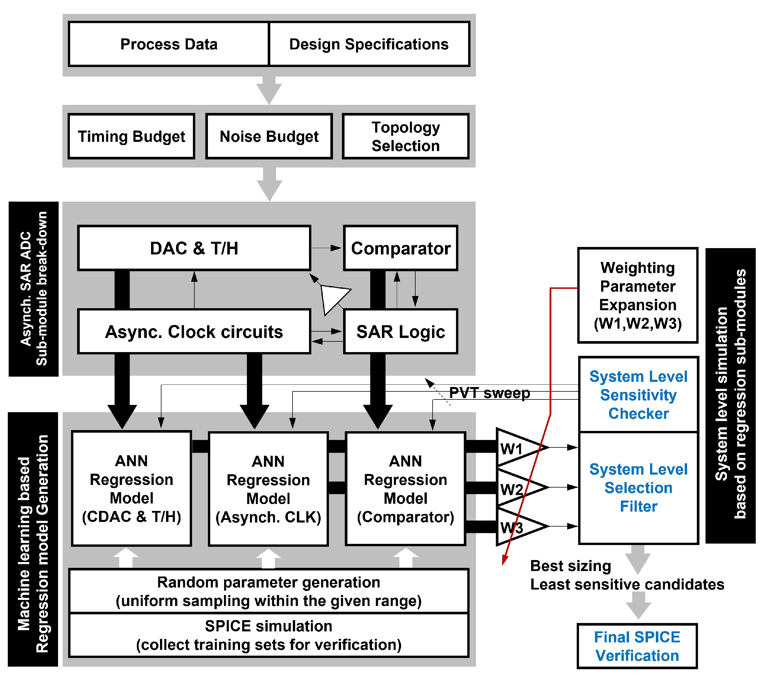
  • We applied the overall design flow to an asynchronous SAR ADC architecture. The asynchronous SAR ADC design is suitable for verifying the performance of the AMS design algorithm because it is quite difficult to determine the optimal performance with respect to the key components of the ADC. Regarding the sensitivity performance, the design example covers the range of the supply voltage deviation of ± 6.25 % , the temperature from −40 C to 80 C, and the process with SS/TT/FF corners. Finally, the figure-of-merit, which indicates the ADC power efficiency, is compared with the results when applying the SPICE-based design method.
The remainder of this paper is organized in the following manner: Section 2 introduces the detailed proposed AMS circuit optimization flow. Section 3 describes a design example employing the proposed design flow. Section 4 presents the simulated results of ADC final performance outcomes considering external condition changes. Section 5 discusses the proposed AMS circuit optimization technique, and Section 6 provides the conclusions.

2. Methods

The overall proposed AMS circuit optimization flow conducts four major steps, as illustrated in Figure 1. Before starting the design flow, the user has to clarify the target circuit (i.e., filter, amplifier, ADC, etc.) and operating conditions. Assuming that the reference design library is well prepared, the main AMS circuit optimization flow performs from a given set of user-defined designs and system constraints. In particular, machine learning techniques (i.e., supervised learning) can be incorporated to identify the least sensitive and co-optimized output designs while building regression models as well as sub-module integration procedures. In the following subsections, four major steps are addressed in more detail.

2.1. Step 1: Preparing a Library

This stage is an initial step for collecting appropriate reference designs for smaller stand-alone modules, such as a unit circuit for a parameterized library. First, each stand-alone module must be accurately evaluated using a fine SPICE simulator, after which it can be used for generating a regression model via a neural network training process. This step is important in terms of building a general-purpose library that can accommodate the various sub-modules that would compose the different target system. This step has to be performed precisely because, if the library is built with inaccurate simulation results, the accuracy of the final result deteriorates further due to the inaccuracy of the regression model.

2.2. Step 2: Creating Sub-Module with User Intent

Based on the system requirements defined by the user, this step divides the user requirements into module-level design constraints employing system design formulas and user preferences, such as those pertaining to occupation and energy efficiency. In this step, we perform supervised learning based on artificial neural networks (ANNs) [23,24,25] to characterize the regression model.

2.3. Step 3: Evaluating Performance and Sensitivity

To deliver reliable circuits, both the user-intended operation condition and the errors that occur during the manufacturing process must be considered. This step includes two main operations: searching for performance changes under the given conditions (e.g., process and temperature variations), and adaptively selecting the least sensitive results within the tolerance level set by the user. Because the cost and time for designing, simulating, and examining all possible operating conditions are limited, this step is challenging. However, given that the proposed design method can shorten the simulation time with its use of the regression model, it enables performance evaluations at a greater variety of operating points.

2.4. Step 4: Generating Final Netlist

Based on the prepared module library and user intents for each module, the selection filter [26] choses the proper modules for each function block, and the generation and validation of a final netlist are performed. Among the various design candidates correspondingly optimized at different operation environments, a top-level selection filter accordingly lists the possible candidates, allowing the user to sign off on the final netlist. As a result, the user-intended AMS circuit can be obtained while not only satisfying the performance matrix but also ensuring robust operation at the target environments.

3. Circuit Design

3.1. Topology Selection: Asynchronous SAR ADC

There are numerous types of AMS circuit topologies; among them, ADC is a viable option here given that it encompasses analog and digital considerations while also stipulating insight into high-speed circuits, such as clocking and high-frequency signaling circuits. When determining which ADC architecture to use, for proper support of the upcoming goal of medium resolutions with a GS/s target, the successive approximation register (SAR) ADC was found to be the best choice for the purposes of this study given its considerable energy efficiency and small footprint. The SAR ADC is primarily a digital type of architecture that therefore scales well in conjunction with feature-size scaling given the straightforward architecture it uses. Typically, the SAR ADC includes a front-end analog circuit with a switched-capacitor sampler (e.g., T/H), a comparator, along with a digital-to-analog converter (DAC) for the subsequent digital circuits.

3.2. Step 1: Preparing a Library

Partitioning the entire circuit architecture into multiple modules is the first step in the regression model-based AMS circuit optimization flow, allowing each module to be easily configured and simulated quickly (as mentioned in Section 2.1). A digital circuit typically consists of a SAR ADC architecture including a few analog blocks, such as a comparator, which is an appropriate candidate for a proof-of-concept, as shown in Figure 2. To evaluate the SAR ADC performance, the figure-of-merit (FoM) index is defined as follows:
FoM = Power dissipation 2 S N D R 1.76 / 6.02 × F s a m p l e ,
S N D R = 10 · l o g 10 P signal P T / H + P comparator + P Quantization .
In this work, the SAR ADC architecture is divided into T/H, timing controller, and comparator circuits, as shown in Figure 2. These three modules are then respectively parameterized to create a module library while covering the target design space. The module library can be simulated with different combinations of parameters to achieve the target performance.

3.3. Step 2: Creating Sub-Module with User Intent

As elaborated in Section 2.2, in order to achieve the precisely desired system-level performance of the final assembly, accurate sub-module characterization is important for every sub-module composing the entire ADC. Each module is considered a ‘black box’ while having a relationship between ‘parameters’ and ‘metrics’. Note that ‘parameter’ presents the group of design inputs, and ‘metrics’ presents the output performance. As the digital circuit can leverage the existing design optimization methods, only a module training process for the analog circuits has been applied. Regarding the given search space during a training process, a smart way to select a ‘training’ set is needed because the module training is not able to cover overall search space. In this work, randomly chosen training samples are used for module characterization, and the range of the training samples is provided by existing known good designs. Based on the 1500 training samples uniformly and randomly selected from the given search space, we created the parameterized module library and collected their output performance metrics using SPICE simulations.
In this work, a neural network comprising multiple hidden layers [27,28] is developed by using the aforementioned training dataset. Moreover, the constructed module library expands the search space of each module for predicting non-present module configurations to compensate for an insufficient training dataset. Depending on the input parameters, multiple input neurons and 30 neurons in the hidden layers are arranged. The number of output neurons is followed by the number of output performance metrics. Consequently, 90% of the dataset was used for the neural network training, and the remaining 10% was used for accuracy validation.

3.3.1. Track-and-Hold Circuit

A transmission gate with a sampling capacitor ( C S ) forms a simple top-plate track-and-hold (T/H) circuit. Since the T/H is a fundamental switched capacitor element, it is an appropriate candidate to which to apply the proposed design methodology. Figure 3a illustrates the non-linear transfer function of the T/H. The linearity performance of the T/H can be enhanced by a properly chosen transmission gate sizing, which results in the highest linearity performance with the reduced non-linear capacitance, as shown in Figure 3b. As a result, the properly selected input parameter with well-defined target output performance metrics enabled us to create the regression model of the T/H circuit. As summarized in Table 1 and Table 2, as input parameters, we defined the ranges of input signal frequency, sampling speed, supply voltage, input signal swing, sampling capacitor, load capacitor, aspect ratio of the transmission gate, process corner, and temperature. The harmonic distortion, the effective number of bits (ENOB), the noise power, and the bandwidth are defined as performance output metrics.
The input signal sampling bandwidth is one of the most important performance indexes in the T/H circuit. The turn-on resistance ( R O N ) values of the transmission gate and attached capacitor C S are dominantly determined by the given input signal bandwidth specification. As the C S size is generally defined by the required thermal noise level (i.e., k T / C ), the turn-on resistance property associated with the practical parasitic determines the dynamic performance of the T/H. According to the operational principle of the T/H, the transfer function in the s-domain ( H T / H ) can be expressed as follows:
H T / H ( s ) = 1 1 + s · R ( V SIG ) · [ C S + C L + C P O + C P ( V SIG ) ]
where the non-linear resistance ( R ) and parasitic capacitance ( C P ) are changed by the magnitude of an input signal V SIG . In this example, there exists a controversial relationship between the non-linear components R and C P . In order to reduce one of non-linear portions, the other portions will grow until an optimum size at which to realize maximum linearity is reached. However, considering process variations, it is difficult to select a sampling switch size that satisfies all the corner conditions. Here, we defined seven input parameters—in this case, the process corners (SS, TT, FF), a supply voltage variation, the input signal common mode voltage, the transmission gate sizes (PMOS, NMOS), the sampling capacitor size ( C S ), and the output load ( C L ). Six output parameters of SFDR and ENOB for all three corners are defined.
Table 3 shows evaluated errors in percentile after different numbers (500, 1000, 1500, and 2000) of training sets of the ANN are used. Here, we used 90% of 4096 randomly generated training references from the SPICE simulation, with the remaining 10% of references used to verify the accuracy. In this sub-module, two hidden layers with ten neurons for each layer and an ELU function [29] as an activation function are applied. The target performance of the T/H circuit is >8 ENOB at all process corners. As shown in Figure 4, even when the other parameters—in this case, the sampling and load capacitance, input common mode level, and supply voltage—are varied, the aspect ratio of 2.75 for the sampling switch mainly contributes to the achievement of peak dynamic performance. Considering the SFDR and ENOB at the optimum points, the T/H performances were not constrained by harmonic distortion.

3.3.2. Comparator

The comparator converts the input voltage into a digital code. Here, the input signal is provided by the front-end T/H circuit or a reference switch network during the SAR charge redistribution procedure. In order to minimize both the active area and power dissipation, a regenerative strong-arm comparator topology is widely used, as shown in Figure 5a. The clocked comparator initially stays in a reset mode ( ENV comp ¯ is off) and then resolves the differential output using a built-in regenerative latch circuit ( ENV comp ¯ is on). Furthermore, we can divide the latter resolving phase into sampling and regeneration phases. The sampling phase begins with the comparator-enabled signal and ends with an established output voltage, which turns on the back-to-back placed regenerative latch. Afterward, the comparator causes the differential output to be fully stretched; thus, one of the comparator outputs is equal to the supply voltage (VDD) but the other decreases to the ground at the end of the regeneration time, as illustrated in Figure 5b. During the regeneration time, the stretched down signal causes the ready signal (RDY) to be flagged; thus, we can measure the comparator resolving time or speed.
Here, we define certain input parameters, including the process corners (SS, TT, FF), a supply voltage variation, grouped and scaled comparator transistor sizes (input, regenerative cross-coupled pairs, and reset switch), load capacitor, and temperature, as summarized in Table 4. Here, the regenerative cross-coupled pairs’ size increases the regeneration strength, and the reset switch is partially related to the noise power level. Moreover, we set the performance output metrics of the comparator (Table 5), the noise power, the power dissipation, and the conversion speed. In comparator design, we can ignore the linearity performance as we are only interested in the polarity against the input signal, and the unit transistor size for the comparator core circuit is selected by an empirical design reference to reduce the search space during the development of the regression model.
Regarding the comparator noise and conversion speed evaluations, we measured the entire circuit noise at different target speeds. According to an analysis of the comparator noise ( P C M P , n o i s e ) and operating speed ( τ C M P ), we found that there is a trade-off relationship between these two output metrics, as follows:
τ C M P α 1 g m V t h I C M P + α 2 C L g m + α 3 l n ( V D D G C M P V I N )
P C M P , n o i s e β 1 8 k T I C M P g m C I N V t h + β 2 2 k T C I N G C M P 2
where g m , C I N , C L , V t h , V D D , I C M P , G C M P , k , and T are correspondingly the transconductance, input and output capacitance, threshold voltage of regenerative pair devices, supply voltage, drain current, comparator voltage gain during the sampling phase, Boltzmann constant, and temperature. The α and β coefficients are topology-dependent scaling constants.
To develop an ANN regression model with the comparator input parameters and output metrics, we trained it more than 2000 times with uniformly and randomly selected training references from the SPICE simulation results. Here, four hidden layers with 16 neurons for each layer and the ELU function activation function are employed due to the increased circuit complexity in comparison with the above T/H example. The target performance of the comparator is a speed of 2 to 2.5 GS/s with more than eight ENOBs at all process corners. Figure 6 shows the ANN regression accuracy of the regenerative strong-arm comparator in terms of the conversion speed (resolving time), power dissipation, and noise power in the CDF expressions. It shows challenges in the areas of the comparator noise model rather than the power dissipation or speed metrics.

3.3.3. SAR ADC Timing Controller

A schematic of an SAR ADC timing controller consisting of variable delay cells is shown in Figure 7. In order to implement an asynchronous SAR operation, the delay cell creates voltage-dependent delayed pulses associated with the supporting digital circuits. The conversion time for a typical N-bit resolution SAR ADC is calculated by adding an input signal tracking-or-sampling time ( T T / H ), a charge redistribution time in capacitive DAC (C-DAC) during the comparator reset period ( T RS ), resolving time of the comparator ( T CMP ), and logic delay time ( T Logic ). A single period of the ADC operation ( T Period ) can be calculated as follows:
T Period = T T / H + i = 1 i = N ( T CMP [ i ] + T RS + T Logic )
T CMP is already covered by the comparator, and T Logic is generally determined once the technology has been decided. Therefore, the remaining T RS must be optimized by selecting the proper size of the delay cell. In contrast with the former circuits, the timing controller behaves as a digital circuit and is relatively simpler in terms of performance predictions. We defined several input parameters, including the process corners (SS, TT, FF), supply voltage variation, scaled logic gate size, load capacitor, and temperature (Table 6). Since the SAR ADC timing controller includes both analog and digital circuits, such as mixed-mode circuits, we can set the aspect ratio (i.e., ratio between width and length of the transistor) and leverage the scaling factor as denoted in a unit of a logic gate size. In addition, the power dissipation, scaled active area, and conversion speed were set as the performance output metrics of the SAR ADC timing controller, as summarized in Table 7. Note that the digital circuit prioritizes the silicon occupation factor since it can be normalized.
The performance of the SAR ADC timing controller is evaluated in terms of its ability to predict the active area, power dissipation, and load condition trade-off, as shown in Figure 8. According to the results shown in Figure 8a, the overall power consumption is increased by larger device size, which would increase the loading capacitor on a driving circuit. Figure 8b shows measured delay variations at ± 100 mV supply voltage change. Although the higher supply voltage would lead to a wide range of controllable delay in time, it requires more power dissipation and undesired delay variations. According to the logic gate size, a duty cycle of the control pulse was evaluated, as shown in Figure 8c. An increasing logic gate size can reduce the pulse duty cycle variation, and an optimum logic gate size can be defined by the first-order derivative of the logic gate size versus the duty cycle variation range relationship.
After the generation of the regression model for the SAR ADC timing controller is complete, delay and duty cycle variations are checked in comparison with the SPICE simulation results. Since an energy-efficient delay controller design eventually saves a large portion of dynamic power dissipation of the entire SAR ADC, a reliable SAR ADC timing controller design with low-power consumption is critical. Therefore, the proper logic gate sizing would be executed by the target user-defined specifications.

3.4. Step 3 and 4: Evaluating Performance and Sensitivity and Generating Final Netlist

In this work, we aim to build a regression model-based circuit design flow. Based on the user intent submitted to the system, the desired design flow automatically selects corresponding modules for the target application. Given the user intents, such as the desired ENOB, the conversion rate, and the required input signal bandwidth, all the module specifications are calculated from the high-level design analysis; thus, the module library can find each candidate in the asynchronous SAR ADC design, as shown in Figure 9. Compatibility is checked through appropriate boundary conditions (i.e., searching for applicable input and output load conditions). Therefore, we follow a design flow to attain the best candidate, using a variety of selection criteria and priorities with respect to the required high-level specifications that users provide. Based on the sensitivity check procedure (mentioned in Section 2.3), a system-level performance variation chart is devised as a result of weight parameter expansion and perturbation. Consequently, the user can choose the desired final netlist (related to Section 2.4). The circuit optimization flow is finally validated against a set of designs by conducting individual performance evaluations.

4. Simulation Results

Figure 10 shows a performance plot from the final verification step in our AMS design flow. The target specification is 8-bit 2-GS/s; thus, the Nyquist input signal bandwidth is 1 GHz. Although the final performance at the Nyquist input frequency is slightly lower than that of the target ENOB, we achieved remarkable energy efficiency (<15 fJ/conversion step), as defined by the figure-of-merit (FoM). Moreover, the final result of the sensitivity check was determined under PVT variations, as shown in Figure 11. According to the process and temperature sweep test to confirm our design flow step 3 and 4 (refer to Section 3.4), the result proves the robust operation of the proposed design given the absence of remarkable performance degradation. However, the supply voltage sweep clearly shows a performance drop at a supply voltage of 0.75 V. This is mainly caused by deterioration of the speed and linearity of the transistor in the front-end T/H circuit, which occurs when the power supply voltage is reduced. Although the achieved ENOB is lower than the target level, the ADC energy efficiency indicates that it has been optimized to perform best in any given situation.
In addition, we prepared three ADC specifications with different ADC resolutions, conversion speeds, and process conditions in order to check whether the proposed optimization method works well for different requirements. Table 8 summarizes and compares the SAR ADC performance of the proposed optimization method with the SPICE simulation results at the different target operating conditions, respectively. Here, the SPICE simulation results (in Table 8) are gold-standard references to evaluate our achieved SAR ADC performance. In essence, the error percentage (in Table 8) represents the accuracy loss in our approach. The proposed AMS optimization technique achieved excellent ADC performance and showed acceptably creditable accuracy. In the comparison of the proposed AMS circuit optimization method and SPICE-based approach, errors of 17.2% and 12.8% can be ignored considering that the ADC FoM generally stays around 15∼20 fF/conversion step in an 8-bit 1.5-GS/s SAR ADC. Other than these errors, the overall accuracy of our proposed approach results is 90% or more.

5. Discussion and Future Research Orientations

By adopting a regression-model-based AMS design flow instead of an expensive SPICE simulator from the initial design phase, the circuit design time can be effectively reduced. However, ambiguities exist when determining the appropriate number of reference samples, especially during the development of known good design-based libraries. Because the performance of an ANN model depends on the number of reference samples, deriving an appropriate number of samples through an empirical study or selecting an effective sampling method can be an important factor in this method. Moreover, uniform input sampling over a given range can degrade the accuracy of the regressor because more training samples are required to approximate a sudden sharp surface. In this work, a manually defined range of input parameters with uniform sampling was inevitably applied to focus more on our AMS design flow. Hence, in order to resolve this limitation, we plan to study the design and application of an adaptive input data sampling algorithm as a future study. In addition, employing a higher-level transfer learning technique would enable our regression-model based optimization flow to be more generalized [30,31,32]; thus, it is expected to create technological synergy, such as dramatically preventing human error.

6. Conclusions

In this research, we propose a regression model-based AMS circuit design optimization flow utilizing parameterized operating conditions. For proof of concept, an asynchronous SAR ADC considering practical environment changes has been successfully evaluated. First, parameterized module library preparation for characterizing module-level operation is performed to apply the scheme to the enlarged design space. Subsequently, a regression model based on an ANN is trained to extract the representative features of modules for the target design space. Afterward, the performance sensitivity is assessed to ensure that the system can meet the user-intended PVT variation target. Lastly, a final performance evaluation at both the module level and the overall system level is done to validate the effectiveness of the proposed AMS design flow. To reflect the design complexity, an advanced technology 14 nm predicted process design kit is used. Given the skewed PVT conditions, the design output successfully shows robust operation of the asynchronous SAR ADC without instances of abrupt performance degradation.

Author Contributions

Conceptualization, J.-W.N.; methodology, J.-W.N.; software, Y.K.L.; validation, J.-W.N. and Y.K.L.; formal analysis, J.-W.N. and Y.K.L.; investigation, J.-W.N. and Y.K.L.; resources, J.-W.N. and Y.K.L.; data curation, J.-W.N., Y.-K.C. and Y.K.L.; writing—original draft preparation, J.-W.N.; writing—review and editing, Y.-K.C. and Y.K.L.; visualization, J.-W.N. and Y.-K.C.; supervision, J.-W.N.; project administration, J.-W.N.; funding acquisition, J.-W.N. and Y.-K.C. All authors have read and agreed to the published version of the manuscript.

Funding

This work was supported by the National Research Foundation of Korea (2021R1G1A1003326), and the EDA tool was supported by the IC Design Education Center (IDEC), Korea.

Conflicts of Interest

The authors declare no conflict of interest.

References

  1. MacMillen, D.; Butts, M.; Camposano, R.; Hill, D.; Williams, T.W. An Industrial view of electronic design automation. IEEE Trans. Comput. Aided Des. Integr. Circuits Syst. 2000, 19, 1428–1448. [Google Scholar] [CrossRef] [Green Version]
  2. Jangkrajarng, N.; Bhattacharya, S.; Hartono, R.; Shi, C.-J. IPRAI—Intellectual property reuse-based analog IC layout automation. Integration 2003, 36, 237–262. [Google Scholar] [CrossRef]
  3. Jespers, P.G.A.; Murmann, B. Systematic Design of Analog CMOS Circuits; Cambridge University Press: Cambridge, UK, 2017. [Google Scholar]
  4. Berkcan, E.; D’Abreu, M. Physical assembly for analog compilation of high voltage ICs. In Proceedings of the IEEE 1988 Custom Integrated Circuits Conference, Rochester, NY, USA, 16–19 May 1988; pp. 14.3/1–14.3/7. [Google Scholar]
  5. Mendhurwar, K.; Sundani, H.; Aggarwal, P.; Raut, R.; Devabhaktuni, V. A new approach to sizing analog CMOS building blocks using pre-compiled neural network models. Analog Integr. Circuits Signal Process. 2012, 70, 265–281. [Google Scholar] [CrossRef]
  6. Nassif, S.R. Modeling and analysis of manufacturing variations. In Proceedings of the IEEE 2001 Custom Integrated Circuits Conference, San Diego, CA, USA, 9 May 2001. [Google Scholar]
  7. Felt, E.; Zanella, S.; Guardiani, C.; Sangiovanni-Vincentelli, A. Hierarchical statistical characterization of mixed-signal circuits using behavioral modeling. In Proceedings of the International Conference on Computer Aided Design, San Jose, CA, USA, 10–14 November 1996. [Google Scholar]
  8. Fraccaroli, E.; Lora, M.; Fummi, F. Automatic Generation of Analog/Mixed Signal Virtual Platforms for Smart Systems. IEEE Trans. Comput. 2020, 69, 1263–1278. [Google Scholar] [CrossRef]
  9. Duran, P.A. A Practical Guide to Analog Behavioral Modeling for IC System Design; Metzler, J.B., Ed.; Springer Science & Business Media: Berlin, Germany, 1998. [Google Scholar]
  10. Rocha, F.; Martins, R.; Lourenço, N.; Horta, N. Electronic Design Automation of Analog ICs Combining Gradient Models with Multi-Objective Evolutionary Algorithms; Springer Briefs in Applied Sciences and Technology; Springer International Publishing: Cham, Switzerland, 2014. [Google Scholar]
  11. Rutenbar, R.A.; Gielen, G.G.E.; Roychowdhury, J. Hierarchical Modeling, Optimization, and Synthesis for System-Level Analog and RF Designs. Proc. IEEE 2007, 95, 640–669. [Google Scholar] [CrossRef]
  12. Koh, H.Y.; Sequin, C.H.; Gray, P.R. OPASYN: A compiler for CMOS operational amplifiers. IEEE Trans. Comput. Aided Des. Integr. Circuits Syst. 1990, 9, 113–125. [Google Scholar] [CrossRef]
  13. Harvey, J.P.; Elmasry, M.I.; Leung, B. STAIC: An interactive framework for synthesizing CMOS and BiCMOS analog circuits. IEEE Trans. Comput. Aided Des. Integr. Circuits Syst. 1992, 11, 1402–1417. [Google Scholar] [CrossRef]
  14. Gielen, G.G.E.; Walscharts, H.C.C.; Sansen, W.M.C. Analog circuit design optimization based on symbolic simulation and simulated annealing. IEEE J. Solid-State Circuits 1990, 25, 707–713. [Google Scholar] [CrossRef]
  15. Swings, K.; Sansen, W. DONALD: A workbench for interactive design space exploration and sizing of analog circuits. In Proceedings of the European Conference on Design Automation, Amsterdam, The Netherlands, 25–28 February 1991; pp. 475–479. [Google Scholar]
  16. Kruiskamp, W.; Leenaerts, D. DARWIN: CMOS opamp synthesis by means of a genetic algorithm. In Proceedings of the Design Automation Conference, San Francisco, CA, USA, 12–16 June 1995; pp. 433–438. [Google Scholar]
  17. Hershenson, M.; Boyd, S.P.; Lee, T.H. GPCAD: A tool for CMOS op-amp synthesis. In Proceedings of the International Conference on Computer-Aided Design, Digest of Technical Papers of the IEEE/ACM, San Jose, CA, USA, 8–12 November 1998; pp. 296–303. [Google Scholar]
  18. Nye, W.; Riley, D.C.; Sangiovanni-Vincentelli, A.; Tits, T.L. DELIGHT.SPICE: An optimization based system for the design of integrated circuits. IEEE Trans. Comput. Aided Des. Integr. Circuits Syst. 1988, 7, 501–519. [Google Scholar] [CrossRef]
  19. Phelps, R.; Krasnicki, M.; Rutenbar, R.A.; Carley, L.R.; Hellums, J.R. Anaconda: Simulation-based synthesis of analog circuits via stochastic pattern search. IEEE Trans. Comput. Aided Des. Integr. Circuits Syst. 2000, 19, 703–717. [Google Scholar] [CrossRef]
  20. Lourenço, N.; Horta, N. GENOM-POF: Multi-Objective evolutionary synthesis of analog ICs with corners validation. In Proceedings of the Fourteenth International Conference on Genetic and Evolutionary Computation Conference (GECCO’ 12), Philadelphia, PA, USA, 7–11 July 2012; pp. 1119–1126. [Google Scholar]
  21. Barros, M.; Guilherme, J.; Horta, N. GA-SVM optimization kernel applied to analog IC design automation. In Proceedings of the IEEE International Conference on Electronics, Nice, France, 10–13 December 2006; pp. 486–489. [Google Scholar]
  22. Nam, J.-W.; Lee, Y. Machine-Learning based Analog and Mixed-signal Circuit Design and Optimization. In Proceedings of the International Conference on Information Networking (ICOIN), Jeju Island, Korea, 12–15 January 2021; pp. 874–876. [Google Scholar]
  23. Van Engelen, J.E.; Hoos, H.H. A survey on semi-supervised learning. Mach. Learn. 2020, 109, 373–440. [Google Scholar] [CrossRef] [Green Version]
  24. Abiodun, O.I.; Jantan, A.; Omolara, A.E.; Dada, K.V.; Mohamed, N.A.; Arshad, H. State-of-the-art in artificial neural network applications: A survey. Heliyon 2018, 4, e00938. [Google Scholar] [CrossRef] [PubMed] [Green Version]
  25. Aizenberg, I.; Belardi, R.; Bindi, M.; Grasso, F.; Manetti, S.; Luchetta, A.; Piccirilli, M.C. A Neural Network Classifier with Multi-Valued Neurons for Analog Circuit Fault Diagnosis. Electronics 2021, 10, 349. [Google Scholar] [CrossRef]
  26. Wu, J.; Chen, X.Y.; Zhang, H.; Xiong, L.D.; Lei, H.; Deng, S.H. Hyperparameter optimization for machine learning models based on Bayesian optimization. J. Electron. Sci. Technol. 2019, 17, 26–40. [Google Scholar]
  27. Al-Saffar, A.A.M.; Tao, H.; Talab, M.A. Review of deep convolution neural network in image classification. In Proceedings of the International Conference on Radar, Antenna, Microwave, Electronics, and Telecommunications (ICRAMET), Jakarta, Indonesia, 23–24 October 2017; pp. 26–31. [Google Scholar]
  28. Bouwmans, T.; Javed, S.; Sultana, M.; Jung, S.K. Deep neural network concepts for background subtraction: A systematic review and comparative evaluation. Neural Netw. 2019, 117, 8–66. [Google Scholar] [CrossRef] [PubMed] [Green Version]
  29. Lau, M.M.; Lim, K.H. Review of Adaptive Activation Function in Deep Neural Network. In Proceedings of the IEEE-EMBS Conference on Biomedical Engineering and Sciences (IECBES), Sarawak, Malaysia, 3–6 December 2018; pp. 686–690. [Google Scholar]
  30. Zheng, J.; Lu, C.; Chen, D.; Guo, D. Improving the Generalization Ability of Deep Neural Networks for Cross-Domain Visual Recognition. IEEE Trans. Cogn. Dev. Syst. 2021, 13, 607–620. [Google Scholar] [CrossRef]
  31. Liu, J.; Hassanpourghadi, M.; Zhang, Q.; Su, S.; Chen, M.S.-W. Transfer Learning with Bayesian Optimization-Aided Sampling for Efficient AMS Circuit Modeling. In Proceedings of the IEEE/ACM International Conference on Computer-Aided Design (ICCAD), Virtual, 2–5 November 2020. [Google Scholar]
  32. Hao, C.; Chen, D. Software/Hardware Co-design for Multi-modal Multi-task Learning in Autonomous Systems. In Proceedings of the IEEE 3rd International Conference on Artificial Intelligence Circuits and Systems (AICAS), Washington, DC, USA, 6–9 June 2021; pp. 1–5. [Google Scholar]
Figure 1. Top-level system diagram of the proposed AMS circuit optimization flow.
Electronics 11 00408 g001
Figure 2. SAR ADC sub-module breakdown and regression models.
Electronics 11 00408 g002
Figure 3. (a) Schematic of sampling network (T/H) and (b) turn-on resistance of transmission gate with different transistor aspect ratios; data from [22].
Electronics 11 00408 g003
Figure 4. (a) T/H circuit’s linearity performance (SFDR) and (b) resolution (ENOB) performance.
Electronics 11 00408 g004
Figure 5. (a) Schematic of comparator and (b) waveform.
Electronics 11 00408 g005
Figure 6. ANN regression accuracy of the comparator.
Electronics 11 00408 g006
Figure 7. Schematic of SAR ADC timing controller consisting of variable delay cells.
Electronics 11 00408 g007
Figure 8. (a) Evaluated area/power dissipation/load (parasitic) relationship of the SAR ADC timing controller, (b) delay change, and (c) pulse duty cycle variation.
Electronics 11 00408 g008
Figure 9. Regression model (ANN)-based asynchronous SAR ADC design flow.
Electronics 11 00408 g009
Figure 10. Performance plots.
Electronics 11 00408 g010
Figure 11. Sensitivity check over PVT variations.
Electronics 11 00408 g011
Table 1. Design input parameters of the T/H module.
Input ParameterVariable RangeUnit
Max[input signal frequency]0.75∼1.2GHz
Sampling speed1.5∼2.5GHz
Supply voltage0.75∼0.85V
Max[input signal swing]1.4Vpp
Sampling capacitor2.0∼30fF
Load capacitor2∼10fF
Aspect ratio[Sampling switch]0.25∼4.0V
Process corner SS , TT , FF -
Temperature−40∼120 C
Table 2. Performance output matrix of the T/H module.
Output MatrixUnit
Harmonic Distortion dBc
ENOBbit
Noise Power V 2
BandwidthGHz
Table 3. ANN regression accuracy of the T/H module (ENOB).
Number of Epoch|Error|Unit
5004.9%
10003.1%
15002.6%
20001.7%
Table 4. Design input parameters of the comparator module.
Input ParameterVariable RangeUnit
Operating speed50∼150psec
Supply voltage0.75∼0.85V
Input transistor size1∼8scale
Regeneration strength1∼8scale
Reset switch size1∼4scale
Load capacitor size2∼10fF
Process corner SS , TT , FF -
Temperature−40∼120 C
Table 5. Performance output metrics of the comparator module.
Output MetricsUnit
Noise power V 2
Poser dissipation W
Speedpsec
Table 6. Design input parameters of the asynchronous clock control module.
Input ParameterVariable RangeUnit
Supply voltage0.7∼0.9V
Logic gate size1∼25scale
Load capacitor size2∼10fF
Process corner SS , TT , FF -
Temperature−40∼120 C
Table 7. Performance output metrics of the asynchronous clock control module.
Output MetricsUnit
Power dissipation W
Areascale
Speedpsec
Table 8. Figure-of-merit comparisons at each target ADC specification; data from [22].
Spec.CornerSPICE Sim.AMS Sim.Error
FoM (fJ/c.s)FoM (fJ/c.s)%
SS6.85.817.2
8-bit 1.5-GS/sTT6.05.59.1
FF5.34.712.8
SS12.511.95.04
8-bit 2.0-GS/sTT9.89.17.7
FF11.89.97.7
SS12.211.83.4
6-bit 2.5-GS/sTT10.09.28.7
FF8.57.710.4
Publisher’s Note: MDPI stays neutral with regard to jurisdictional claims in published maps and institutional affiliations.

