Review

A Survey on Capacitor Voltage Control in Neutral-Point-Clamped Multilevel Converters

1
Tecnocampus, Universitat Pompeu Fabra, 08302 Mataró, Spain
2
Electronic Engineering Department, Universitat Politècnica de Catalunya, 08028 Barcelona, Spain
3
Departament d’Enginyeries, Universitat de Vic, 08500 Vic, Spain
4
Institut de Recerca en Energia de Catalunya, 08930 Sant Adrià del Besòs, Spain
5
Department of Electrical & Electronic Engineering, University of Bristol, Bristol BS8 1UB, UK
6
Department of Electronic Engineering, Universidad Técnica Federico Santa María, Valparaíso 110-V, Chile
*
Author to whom correspondence should be addressed.
Electronics 2022, 11(4), 527; https://doi.org/10.3390/electronics11040527
Submission received: 10 December 2021 / Revised: 2 February 2022 / Accepted: 5 February 2022 / Published: 10 February 2022
(This article belongs to the Special Issue 10th Anniversary of Electronics: Recent Advances in Power Electronics)

Abstract

:
Neutral-point-clamped multilevel converters are currently a suitable solution for a wide range of applications. It is well known that the capacitor voltage balance is a major issue for this topology. In this paper, a brief summary of the basic topologies, modulations, and features of neutral-point-clamped multilevel converters is presented, prior to a detailed description and analysis of the capacitor voltage balance behavior. Then, the most relevant methods to manage the capacitor voltage balance are presented and discussed, including operation in the overmodulation region, at low frequency-modulation indexes, with different numbers of AC phases, and with different numbers of levels. Both open- and closed-loop methods are discussed. Some methods based on adding external circuitry are also presented and analyzed. Although the focus of the paper is mainly DC–AC conversion, the techniques for capacitor voltage balance in DC–DC conversion are discussed as well. Finally, the paper concludes with some application examples benefiting from the presented techniques.

1. Introduction

The neutral-point-clamped (NPC) multilevel converter [1,2,3,4,5,6] is nowadays a mature technology that has become established as a standard topology for a number of applications, at a wide voltage and power range [7,8,9,10], in recent decades.
The advantages and drawbacks of voltage-source multilevel converters in comparison with conventional two-level converters have been extensively detailed in the literature [8,10,11,12,13,14,15]. The main advantages are: lower device voltage rating, reduced harmonic distortion, reduced common mode voltage, enhanced power losses distribution in the converter, and higher efficiency. These advantages are obtained at the cost of increasing the number of semiconductors and passive components, and also requiring higher modulation and control complexity.
There are three basic multilevel topologies [9,12,13,14,16,17,18]: NPC, flying capacitor, and cascaded H-bridge. Starting from the original version of these basic topologies, a number of different multilevel topologies have been developed, such as the modular multilevel converter [19], the stacked multicell converter [20], the multilevel active-clamped converter [21], and reduced switch count converters [22].
In comparison to other multilevel topologies, the NPC family needs only one common DC voltage source for all converter legs and presents the advantage of being implemented with a full semiconductor layout, as the required capacitors are placed outside the converter legs; that is, no passive components, usually bulky in comparison with the semiconductors, are inside the converter legs. This feature enables the possibility of compacting the converter implementation, reducing volume, and increasing the power density. However, the main drawback of the NPC topology [3] is the requirement to keep the capacitor voltages balanced [4,16]. This survey provides a review of the solutions proposed in the literature to overcome this specific drawback.
The area of application of multilevel converters and, among them, the NPC converters, has expanded over the years. In earlier years, around the 1990s, multilevel converters were intended for high-voltage and high-power applications [13,23], with power semiconductor technology available at that time. Since then, technical evolution has provided enhanced power semiconductor technologies, faster digital processors to implement modulation and control, and thousands of technical papers providing a deeper knowledge about the multilevel converter operation. This development has made multilevel converters suitable not only for high voltage and high power but also for low–medium voltage and power applications [24,25,26,27,28,29]. For high-voltage and high-power applications, the lower device voltage rating is the most valuable feature of multilevel converters. Instead, in low–medium voltage and power applications, the focus is put on taking advantage of its inherent enhanced voltage and current quality, higher efficiency and better power loss distribution.
Therefore, as a result of the current state of the technology, the NPC is at present one of the most implemented multilevel topologies, mainly in DC–AC converters. The conventional operation of a NPC converter requires that the DC capacitor voltages be equal (balanced) to VDc/(n − 1) at any time and in any operation conditions [3,4,30], where V D C is the total DC-link voltage and n is the number of levels. If this requirement is not verified, on one hand, some power semiconductor devices withstand a higher off-state voltage that could lead to overvoltage failure, and on the other hand, unbalanced voltages could also generate output voltage distortion. In the most typical case, the operation of the NPC converter is not allowed if the DC capacitor voltages are unbalanced. Therefore, some actions should be included in the switching strategy and/or control of the NPC converter to achieve the required DC capacitor voltage balance.
The NPC converter capacitor voltage balance depends on several factors [30,31], such as the amplitude modulation index, the frequency modulation index and the load power factor. Moreover, a higher number of levels, which can enhance the converter voltage and current quality, will increase the difficulty to balance the capacitor voltages. Even more, some applications can benefit from operating with a capacitor voltage imbalance that must be controlled [32,33]. That is, the capacitor voltage balance issue is complex and not straightforward.
As most of the applications of the NPC multilevel converters are for DC–AC conversion, the present survey is focused mainly on this type of power conversion. However, as NPC multilevel converters are also suitable for DC–DC conversion, the capacitor voltage balance for DC–DC conversion is also addressed in a specific section.
This survey reviews and summarizes the modulations, control strategies, and circuits proposed by many researchers to deal with the NPC multilevel converter capacitor voltage balance, which seems not to be covered previously in the literature. The paper is organized as follows. In Section 2, the fundamentals of NPC multilevel converters are described. The NPC capacitor voltage balance is analyzed in Section 3. Open- and closed-loop balancing methods are reported in Section 4 and Section 5, respectively. Section 6 shows some hardware-based balancing methods. Balancing techniques for the NPC DC–DC conversion case are described in Section 7. Section 8 presents some cases where the NPC converter operates under a controlled unbalanced condition, which some applications can take advantage of. Finally, conclusions are provided in Section 9.

2. Fundamentals of NPC Multilevel Converters

The fundamentals of NPC multilevel converters are briefly described in this section, including the functional diagram and operating principles, the main topologies, a basic summary of the modulations, and other basic control methods without a modulator.

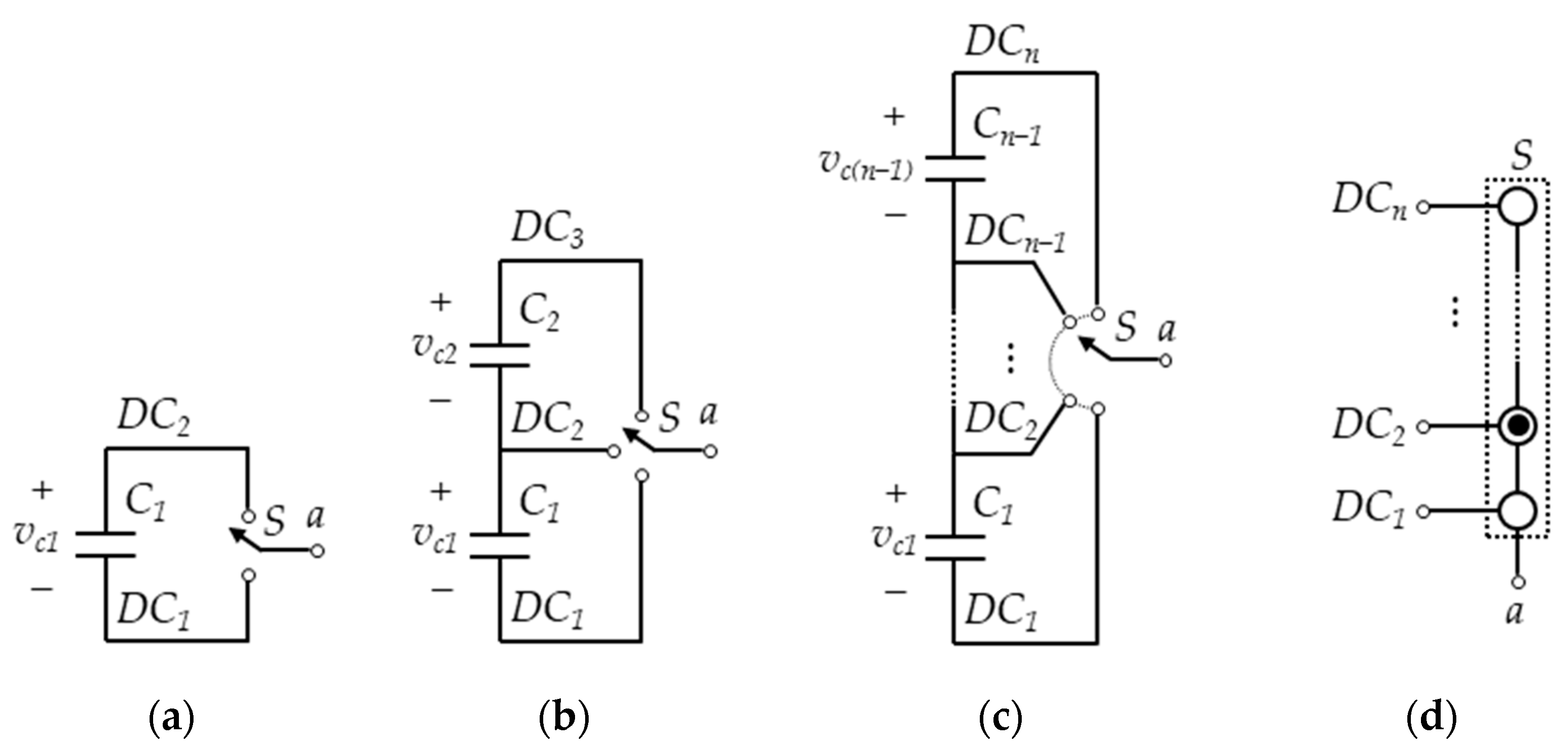
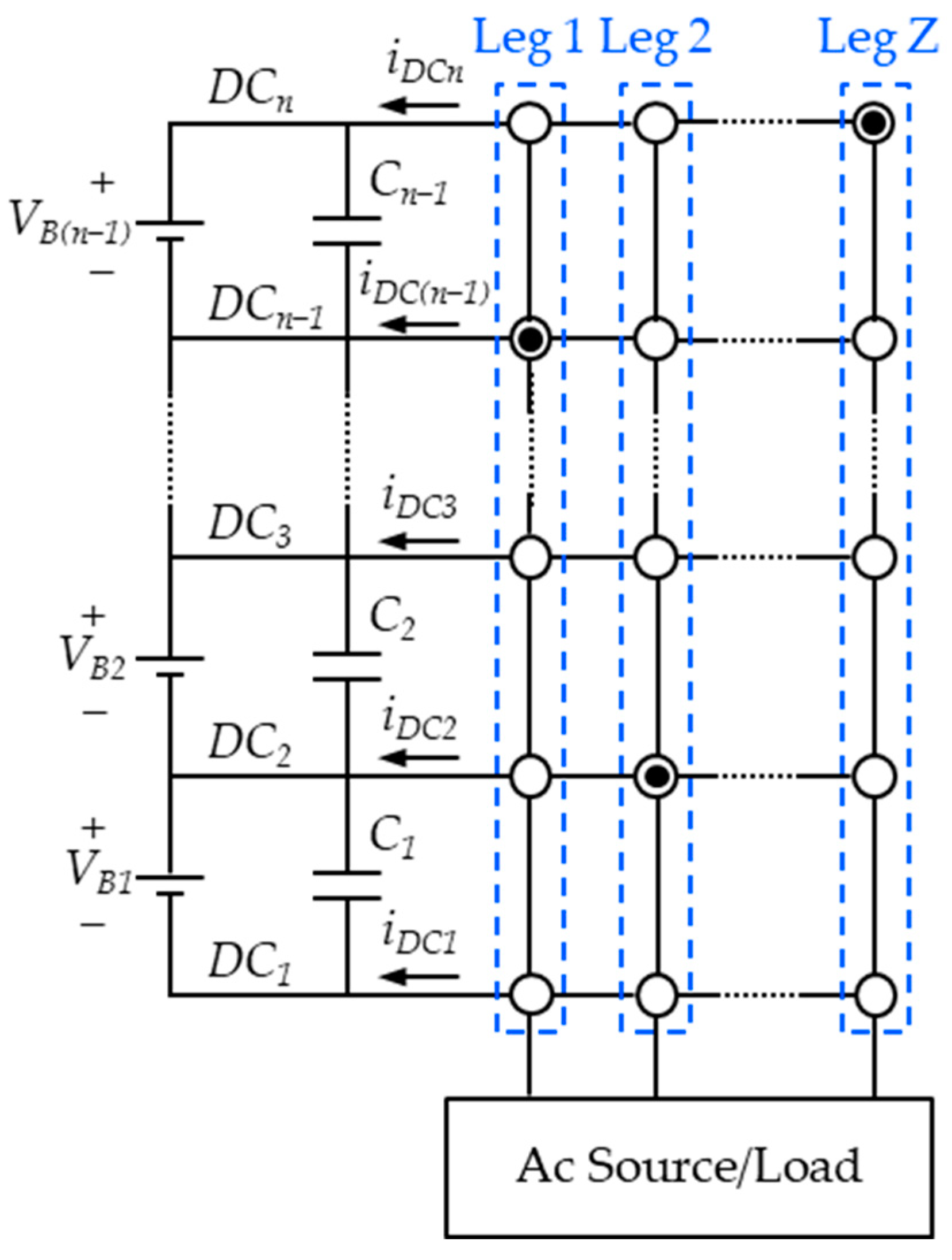
2.1. Functional Diagram and Operating Principle

The operation of the NPC multilevel converter is extensively reported in the literature [2,4,12,13,14,16]. Figure 1 depicts a basic functional diagram for one leg of a NPC multilevel converter. The DC-link is split by (n − 1) series connected capacitors, thus the total DC-link voltage (VDC) is the sum of all the capacitor voltages Vci.
V D C = i = 1 n 1 v c i .
When the capacitor voltages are balanced, each capacitor voltage is Vci = VDc/(n − 1). The output of the leg can be connected to any of the outer DC-link points and to any of the intermediate points created by the series connection of the capacitors, usually known as neutral points, by means of a proper power semiconductor arrangement and control, represented in Figure 1 as an ideal commutator. Therefore, depending on the position of the commutator, the output voltage can present n different values (levels). For instance, for the 3-level leg shown in Figure 1b, the output voltage can take n = 3 different voltage levels with reference to DC1 (0, Vc1 = VDC/2, Vc1 + Vc2 = VDC). Figure 1c,d shows equivalent symbols for the n-level NPC converter leg.
The NPC multilevel converters present a set of advantages [4,14,26]:
  • The passive energy storage components such as capacitors and inductors are placed outside the power semiconductor array, enabling compact converter implementations with higher power density.
  • Since the power devices only have to block VDC/(n − 1) voltage, typically, it enables higher converter DC-link voltage and power ratings.
  • Reduction of switching losses [15,34]: (i) since switching transitions take place at lower blocking voltage VDC/(n − 1); and (ii) lower voltage-rated devices have lower switching losses, typically.
  • Reduction of the output AC voltage harmonic distortion, hence the output filter size is smaller (if required); lower converter AC-side common-mode voltage [35,36]; and lower electromagnetic noise [15].
  • Enhanced fault-tolerance capacity, because of the increased redundancy, since the failure of one device does not inevitably lead to a full leg shutdown [37,38].
  • Better loss sharing among converter devices, improving the temperature performance of the converter and, subsequently, enhancing its reliability [39].
  • Since multiple voltage levels are available at the DC-link, it enables the implementation of a specific control for each DC-link voltage level, which may allow a more efficient control of the power flow between systems [32,33].
However, NPC multilevel converters show two main drawbacks:
  • The number of power semiconductor devices increases significantly with the number of levels.
  • Typically, the DC-link capacitor voltages must be kept balanced at all time [16]. Unbalanced DC-link capacitor voltages cause some power devices to block more than one voltage level VDC/(n − 1), which is unacceptable in most cases as it can lead to a device overvoltage failure. Moreover, it typically generates low-frequency output voltage distortion [40,41].
Some applications of NPC multilevel converters are motor drives [23,42,43], photovoltaic power generation [32,44,45,46], wind power generation [47,48,49], static synchronous compensation [10,50], and DC–DC conversion [29,51].

2.2. Topologies

The four main NPC topologies are depicted in Figure 2, taking the 4-level case as an example, although the extension to the n-level case is straightforward [4]. Other NPC topologies can be obtained by modifying or combining these basic topologies [52].
Note that, at present, the commercial versions of NPC converters are limited to the 3-level case [10]. However, this survey addresses the generic n-level case, as it is expected that NPC converters with higher number of levels will be commercially applied in the near future.
Figure 2a shows the diode-clamped topology, which refers to the pioneer NPC topology [1,5], which is the most popular topology. It is well known that, for n > 3, some of the clamping diodes in this topology are required to block more than one voltage level VDC/(n − 1), making necessary a series connection of diodes per position [16], which may hinder the implementation of this topology [13].
To overcome the abovementioned drawback, the diode-clamped topology is modified by adding supplementary clamping diodes and inner connections [6], as shown in Figure 2b. There is no need for series connection of clamping diodes in this modified diode-clamped topology, since all the semiconductors block one voltage level [4]. However, the topology does not guarantee inherently this blocking voltage for all components, and some additional circuitry may be required [6].
In the diode-clamped topology, the loss distribution among the converter power devices is unequal, causing unsymmetrical temperature distribution of the semiconductor junction [53]. This shortcoming can be alleviated by using the active NPC (ANPC) topology [21,39,53,54] depicted in Figure 2c. Starting from the modified diode-clamped topology [6], Figure 2b, transistors are placed in parallel with the clamping diodes, resulting in the ANPC topology shown in Figure 2c. In this topology, the additional transistors enable redundant current paths that enhance the power loss distribution. Moreover, the ANPC topology guarantees the same blocking voltage value VDC/(n − 1) for all devices [4,21].
There is an obvious interest in reducing the large number of semiconductors required by multilevel topologies. The reduced active-clamped topology [2,55] shown in Figure 2d is a popular topology with a reduced number of semiconductors, at the expense of increasing the blocking voltage value of some devices beyond one voltage level [4]. This topology is also known as T-type [27,56] or π-type [57,58] topology for the 3-level and 4-level cases, respectively.
It is worth highlighting that, whatever the topology used to implement the NPC multilevel converter legs, the operation of the leg can be reduced to the functional schemes depicted in Figure 1c,d.

2.3. Modulations

The most conventional control method for power electronics converters consists of a controller (a proportional-integral controller, in many cases) which generates the reference voltage input to a modulator. In this subsection, a basic summary of the modulations for NPC multilevel converters [4,9,10] is presented. Modulations for DC–AC conversion are mostly considered, although a brief overview of DC–DC conversion is also given at the end of this subsection.
Figure 3 shows a simple classification for multilevel modulations. Modulations that synthetize a given reference AC voltage can be broadly divided into two different subgroups, for low and high switching frequency.

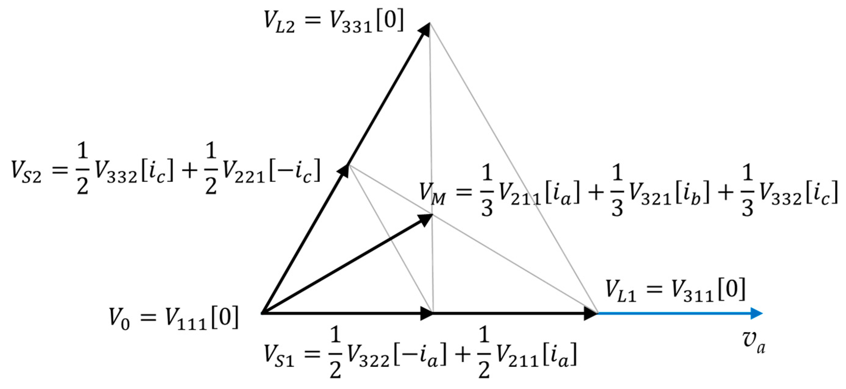
2.3.1. Space Vector Control

At every point in time, the space vector closest to the reference vector is selected and applied in the converter [59]. Figure 4a shows the space vector diagram for a 5-level three-phase converter, where the steady-state circular reference vector trajectory is depicted in dashed red. The different space vectors selected for this specific reference vector trajectory are highlighted in red. The output voltage generated with this modulation is not able to follow the fundamental reference voltage, presenting steady-state error and low-order harmonics. It is mainly intended for converters with a very high number of levels.
This strategy can also be implemented on a per leg basis through selecting the leg AC terminal voltage closest to the reference voltage, as shown in Figure 4b. In this case, the strategy receives the name of nearest-level control [16].

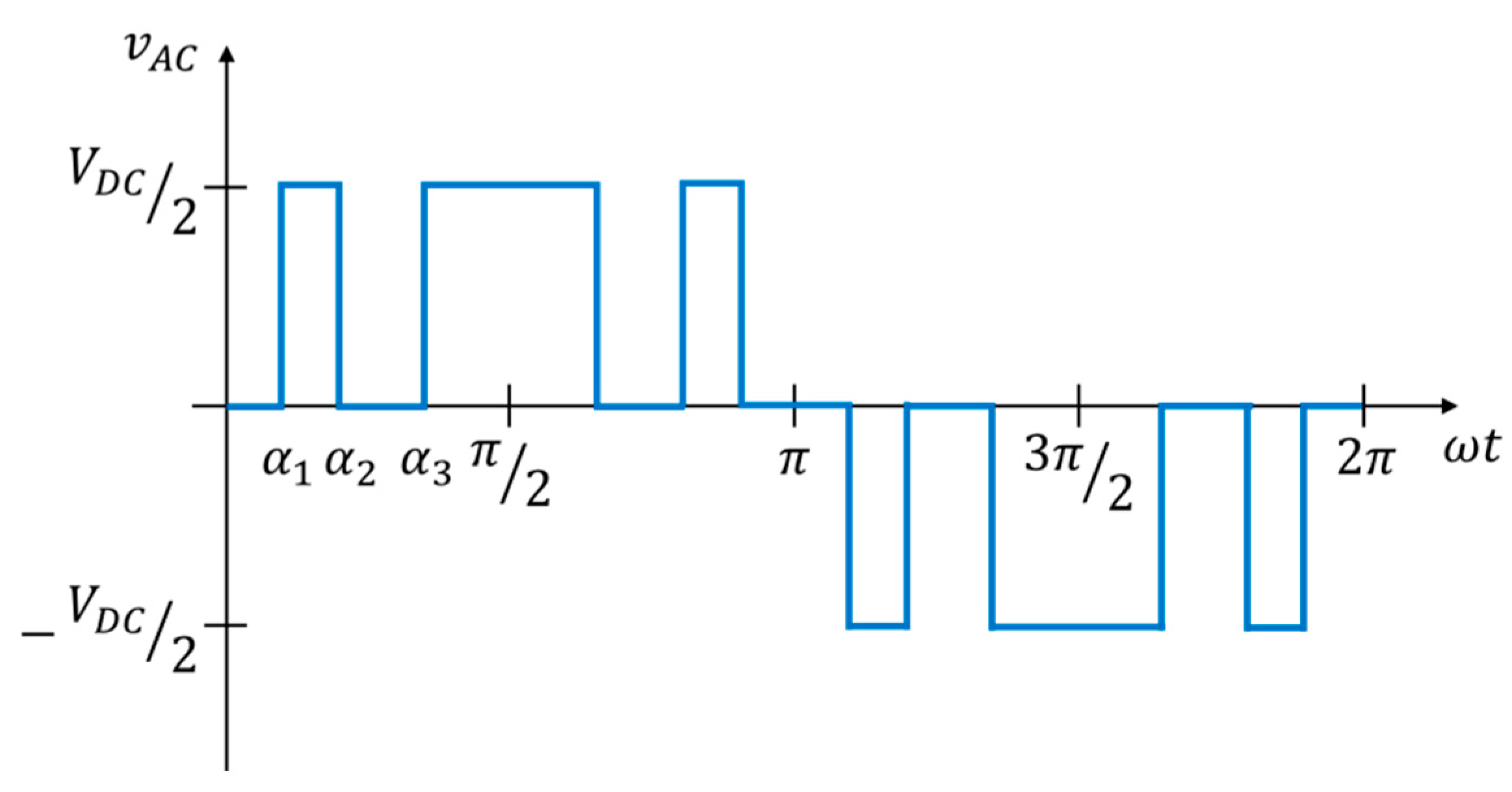
2.3.2. Programmed Pulse Width Modulation (PWM)

The leg AC terminal voltage waveform is approximated by means of a PWM waveform with quarter-wave symmetry, specified by means of k independent switching angles [2]. Figure 5 presents an example of a 3-level converter, with k = 3, where α1, α2 and α3 are the switching angles. One of the switching angles is used to obtain the desired fundamental component voltage amplitude. The remaining switching angles can be used for other purposes, typically to eliminate (k – 1) output voltage harmonics, which is known as selective harmonic elimination (SHE) [60].
This strategy requires the offline calculation of the solution to the nonlinear system of equations to find the switching angles, and its real-time application with a look-up table. As k increases, the harmonic content of the output voltage waveform improves, but the calculation of the angles becomes more complex, leading even to a lack of solution. Moreover, this modulation strategy leads to closed-loop controls with reduced dynamic performance [61].

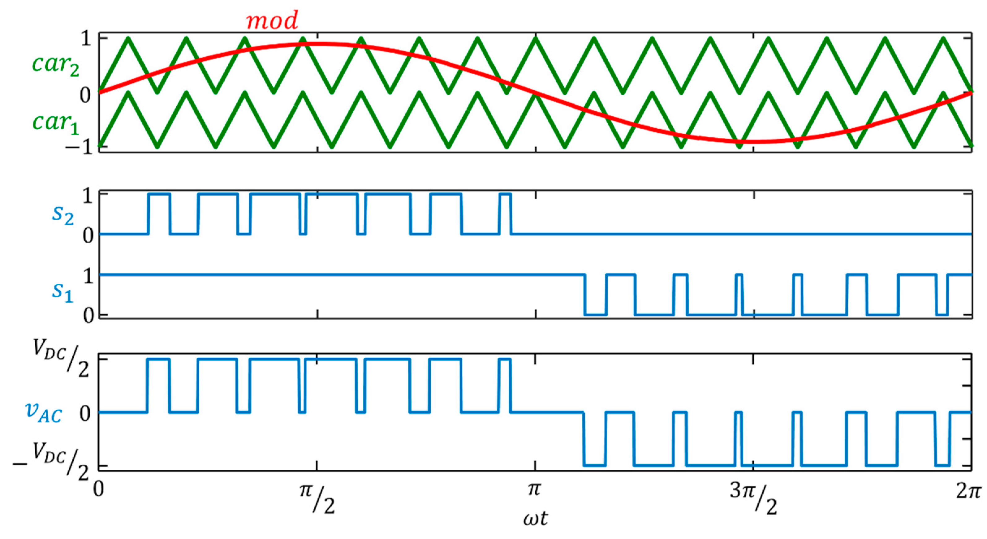
2.3.3. Carrier-Based PWM

This strategy is the natural extension of the carrier-based bipolar PWM [61] to multilevel converters [5,9,10,62]. In its simplest form, the n-level case requires one sinusoidal modulating waveform and (n − 1) carriers per leg, where each carrier is placed between two voltage levels. Hence, this modulation is also known as level-shifted PWM. The level-shifted carriers can present a different phase shift [63], although the best output voltage harmonic content is obtained with no phase shift. As an example, Figure 6 shows this modulation for a 3-level converter, where one sinusoidal modulating waveform and two level-shifted carriers per leg are used. The modulating signals of all legs are phase-shifted, 2π/p where p is the number of legs. At every point in time, the leg position is given by the number of carriers below the modulating signal, and the switch control signals S1, …, Sn are obtained by comparison of the modulating signal with each of the carriers.
This modulation has been commonly used in the industry, since it gathers simplicity and good performance [24].

2.3.4. Space Vector Modulation (SVM)

Power electronics converters have a finite number of possible switching states that provide a finite number of discrete output voltages, where each one can be represented by means of its corresponding voltage space vector. By means of a linear combination of the converter space vectors, the SVM strategy generates an average output voltage vector equal to the reference output voltage vector over one switching period [64].
The number of space vectors increases significantly with the number of levels [65,66], together with the number of redundant switching states (different switching states with the same space vector). Therefore, multilevel converters have available many options, with several degrees of freedom, to select the space vectors used for the linear combination that generates the output voltage vector. Hence, space vectors are usually selected to pursue some additional operation goals. For instance, the number of switching transitions can be minimized by selecting the minimum possible number of space vectors [4]. The output voltage harmonic distortion can also be minimized by selecting the space vectors closest to the reference, a strategy known as the nearest three vectors (NTV−SVM) [66,67]. Figure 7 depicts an example of the NTV−SVM, where the nearest three vectors (V1, V2, and V3) to the reference voltage V* are selected.
Another possible space vector selection is the so-called virtual vector SVM (VV−SVM) [68]. In this strategy, the output voltage vector is generated by a linear combination of virtual space vectors, which are defined by the user as a linear combination of certain converter switching states. Among other advantages, this modulation is particularly useful to balance the capacitor voltages [69,70].
A three-dimensional SVM (3D−SVM) [71,72] is applied mainly in unbalanced three-phase systems.
It is worth highlighting that SVM strategies have a carrier-based PWM equivalent [73,74,75,76,77,78], with a suitable common-mode component added to the modulating signals, or even the introduction of multiple modulating signals per phase. The only difference between both modulations is found in the procedure to determine the gating signals of the converter switches: in SVM, the converter is considered as a whole; in carrier-based PWM, each phase is considered separately [61].
The SVM technique offers flexibility and capacitor voltage balancing, although the computation burden grows as the number of levels increases. However, new calculation algorithms with reduced computation burden allow us to overcome this drawback [7].

2.3.5. Modulations for DC–DC Conversion

At present, there are few applications of NPC multilevel converters to DC–DC conversion. However, some modulations are found in the literature for NPC multilevel DC–DC converters, without galvanic isolation [79], and with galvanic isolation [80,81].

2.4. Control Methods without a Modulator

Unlike conventional control techniques for power electronics converters (controller + modulator), some control methods do not require a modulator. These control methods directly determine the corresponding switching state of the converter, without a modulator, to pursue the system control goals. In this subsection, these kinds of control methods are briefly described.
Hysteresis control is the strategy used in direct torque control (DTC) [82] and direct power control (DPC) [83]. When the controlled system variable goes outside the hysteresis band limits, the converter switching state changes to redirect the variable back inside the hysteresis band.
In predictive control and, more specifically, in finite-control-set model predictive control, the error of the controlled variables and eventually other performance indicators are included in a cost function by means of the mathematical model of the system. In every switching period, the cost function is evaluated for all the switching states of the converter, and the switching state that minimizes the cost function is selected and applied in the following switching period [47,48,84].
A relevant drawback of both strategies is their variable switching frequency and spread harmonic spectrum, although it can be mitigated by introducing some strategy modifications [85,86].

3. Analysis of the Capacitor Voltage Balance

As shown in Figure 1, the DC-link of the n−level NPC converter is split by (n − 1) series-connected capacitors, typically with the same capacitance (C1 = C2 = ‧‧‧ = Cn−1). Proper converter operation requires the capacitor voltages to be balanced; i.e., all the capacitor voltages should be vCi = VDC/(n − 1)at all times.
Since the converter legs are often connected to the inner DC-link points (neutral points), the ordinary operation of the converter causes the circulation of current through the DC-link neutral points, which modifies the capacitor voltage balance. Figure 8a shows the 3-level case, where the relationship between the neutral-point current i D C 2 and the derivative of the capacitor voltage imbalance v i m b = v C 2 v C 1 is deduced as
i D C 2 = i c 2 i c 1 = C 2 · d v c 2 d t C 1 · d v c 1 d t = C · d ( v c 2 v c 1 ) d t = C · d v i m b d t .
Figure 8b shows the extension to the general n-level case, where only the influence of the current through the neutral point k is considered. The neutral-point current i D C k is proportional to the derivative of the imbalance voltage v i m b k between the average voltage of the ( n k ) top DC-link capacitors v c k u / ( n k ) , and the average voltage of the bottom ( k 1 ) capacitors v c k d / ( k 1 ) , according to
i D C k = i c k i c ( k 1 ) = C n k · d v c k u d t C k 1 · d v c k d d t = C · d ( v c k u n k v c k d k 1 ) d t = C · d v i m b k d t .
Starting from a capacitor voltage balance condition, it is deduced from (3) that the DC-link capacitor voltage balance is kept when all the DC-link neutral-point currents are zero; that is, when no charge is provided or extracted through the neutral points [87].
For a n-level converter, the DC-link capacitor voltage balance condition is obtained by applying (3) with i D C k = 0 to all the ( n 2 ) DC-link neutral points [87].
Since the converter legs are often connected to the DC-link neutral points, the ordinary operation of the converter does not allow obtaining zero instantaneous currents through the DC-link neutral points at all times, leading unavoidably to capacitor voltage imbalance. Nevertheless, considering a given period of time and by means of a proper method, it is feasible to get zero average neutral-point currents. In this case, a zero net charge flows through the neutral points, and therefore the average capacitor voltage balance is kept. Note that, within the considered period, the instantaneous neutral-point currents cause capacitor voltage ripple, the amplitude of which depends on the neutral-point current value, the capacitor value, and the length of the period considered for averaging. That is, average capacitor voltage balance can be achieved, but some transient imbalance is present (capacitor voltage ripple). With the same capacitor value, the higher the neutral-point currents and the longer the period, the higher the capacitor voltage ripple and transient imbalance amplitude.
The DC-link capacitor voltage balance depends on the neutral-point current’s behavior which, in turn, depends strongly on the modulation strategy of the converter. Hence, although a generalized analysis is feasible, a modulation strategy is required to achieve proper detail and quantification. Therefore, in the literature, the analysis of the capacitor voltage balance in NPC multilevel converters is mostly related to a specific modulation as, for instance, 3-level PWM [88], n-level PWM [89], 3-level SVM [40], 3-level VV−SVM [69], 4-level VV−SVM [90], 3-level SHE [91], n-level SHE [92].
To illustrate the charge/discharge of the DC-link capacitors, a simple analysis of the neutral-point current ( i D C 3 ) in a 4-level NPC leg is shown in Figure 9a, operating with a simple space vector control strategy and assuming a sinusoidal output current. In the case of the unity power factor, as depicted in Figure 9b, the output current is in phase with the output voltage and the neutral-point current i D C 3 presents only positive values. Hence, in this case, the average value of i D C 3 is always positive, leading to a DC-link capacitor voltage imbalance. Figure 9c shows the case with an output current lagging 90° from the output voltage. In this case, the neutral-point current i D C 3 has the same positive and negative waveform, and zero average value, therefore the balance is kept. With this modulation strategy, only active currents have influence on imbalance [93].
In a multiphase system, the analysis can be performed in the space vector diagram. The neutral-point current is shown for each switching state for the 3-level three-phase NPC in the diagram depicted in Figure 10. From Figure 10 and (2), it is simple to deduce the trend of the DC-link voltage balance for each switching state. Zero and large vectors do not have influence on the balance. Small vectors can be generated by two redundant switching states having the same but opposite influence on the balance. Medium vectors have influence on the voltage balance but they do not have any redundant switching state. This simple analysis can be directly extended from 3- to n-level.
As detailed above, the DC-link capacitor voltage balance is achieved when the average currents through all the neutral points are zero. It is worth highlighting the significance of the setting of the averaging period length to calculate the average neutral-point currents. It can be set from a switching period to a line period, or even longer. A shorter averaging period causes smaller charge flowing through the neutral points, yielding smaller voltage ripple, and allowing the use of smaller DC-link capacitors. When a longer averaging period is used, bigger DC-link capacitors are required to avoid a large voltage ripple amplitude, but the method to maintain the balance can be simpler. Note that higher voltage ripple amplitude could lead to an excessive blocking voltage in the switching devices [31] and significant output AC voltage distortion [94,95].
The implementation of a balancing method is essential to control the average neutral-point currents and consequently to guarantee the capacitor voltage balance, at all times. Note that the balancing method should be used to keep the balance, starting from a balanced condition, and must also have the capacity to take the system to a balanced condition, starting from an unbalanced condition. If no balancing method is considered in the converter control, the DC-link capacitor voltage balance can be kept only in a very reduced number of cases and operating conditions [96,97,98], since the converter itself has a limited capability to maintain the balance. Even in these most favorable cases, the average neutral-point currents may take non-zero values if the switching pattern presents some imbalance, or during transient operation, which may lead to DC-link capacitor voltage imbalance [88,99].
A classification of the solutions for DC-link capacitor voltage balancing is shown in Figure 11. Software solutions consist of properly adapting modulations and/or control methods to guarantee the balance, which can be implemented on an open-loop or closed-loop basis. Hardware solutions consist of adding additional circuitry. These solutions are described in the following sections.

4. Open-Loop Techniques

There are a set of methods that pursue the DC-link capacitor voltage balance which can be classified as open-loop techniques. Typically, these techniques analyze the unbalance problem considering the specific modulation strategy used in each case, and then propose certain arrangements over the modulation strategy to keep the balance. Good balance behavior can be reached in some cases. However, the lack of feedback inherently limits the ability to compensate for the imbalance.
The selection of the NPC converter voltage vectors is usually done to provide the best output voltage quality, the smallest number of commutations (to minimize switching losses), and to keep the balance, where the use of the redundant switching states is essential. To reduce switching losses, early modulation strategies for NPC converters employed a set of rules to restrict the selection of the switching states, such as for instance allowing only commutations between two adjacent voltage levels (carrier-based PWM) or by using the nearest three vectors (NTV−SVM).
As observed in Figure 10, and extensively in the n-level cases, when using conventional SVM techniques, as the modulation index increases, larger voltage vectors are required to generate the output voltage. This creates a lack of redundant switching states, making unattainable the balance within the switching period [100,101,102]. This difficulty varies depending on the load conditions (load power factor and harmonic content).
In the case of a 3-level three-phase NPC AC–DC converter, balanced operation within a switching period cannot be achieved for fairly high modulation index values and low load power factors. A low-frequency ripple (1/3 of the line frequency) appears in the neutral points [40]. That is, balance is not possible within the switching period, but can be achieved within a longer period at the expense of having higher voltage imbalance ripple amplitude [103]. This ripple causes, on one hand, higher blocking voltage in the semiconductor devices and, on the other hand, as the ripple propagates from the DC side to the AC converter side, output voltage distortion [40,104].
In the case of a n-level three-phase NPC DC–AC converter, with n 4 , to keep balanced operation within a switching period, it must be verified that [101]
m < 0.551 | cos φ | .
where φ is the load phase angle and m is the modulation index, defined as the peak value of the fundamental line-to-line voltage divided by the total DC-link voltage. For a modulation index higher than (4), some of the capacitor voltages collapse, which results in a critical system failure. This boundary for balanced operation is depicted in Figure 12a. In Figure 12b, this boundary is shown over a space vector diagram of a 5-level three-phase converter.
In a modulation, there is usually freedom to adjust the zero-sequence voltage. As the neutral-point currents are related to the zero-sequence voltage [105], this degree of freedom is used as an open-loop balancing technique [31,40,88,105], although the balance is not achieved for the full operation range.
The VV−SVM switching strategy synthesizes the output voltage from a set of virtual voltage vectors defined as a linear combination of the vectors corresponding to certain switching states. All the virtual voltage vectors are defined to have an associated switching average neutral-point current equal to zero, as detailed in Figure 13. Thus, whatever set of voltage vectors is used to generate the output voltage, no imbalance is introduced. The VV−SVM strategy is capable of controlling the DC-link capacitor voltage balance for any load, modulation index and number of levels, provided that the addition of the output three-phase currents equals zero, as detailed for 3-level [69,70], 4-level [90], n-level [106], n-level two-leg [107], with optimized spectral performance [108] and with implementation as a carrier-based PWM for n-level n-leg NPC [109]. The extension to the overmodulation region is found in [110,111]. Because of the virtual voltage vector definition, the VV−SVM presents a higher number of commutations (about 4/3, for n = 3) per switching period than the conventional NTV−SVM. However, VV−SVM may present a similar device junction temperature stress compared to a conventional NTV−SVM, thanks to its better switch utilization [112].
Other alternative PWM strategies have been also defined to achieve capacitor voltage balance under a number of levels n ≥ 4, such as carrier-overlapped PWM [89,113,114]. The balancing is guaranteed on average over the line cycle for all modulation index values and with lower commutations than with the VV-SVM.
Hybrid modulations [41,115] take advantage of the benefits of each modulation. For instance, for m < 0.5 NTV−SVM can be used to reduce commutations, and for m > 0.5 VV−SVM can be used to assure the balance, at the expense of increasing commutations.
Finally, note that, under certain operating conditions, balance can be kept by means of the natural balancing mechanisms of the NPC converter. This “do-nothing” control is known as natural balancing [96,97] or self-balancing [92,98]. However, the requirements to keep the balance by natural balancing are very restrictive. For NPC converters, natural balancing seems to be reported in the literature only for the 3-level [92,97,98], and the extension to a higher number of levels is apparently not feasible. It is also strongly sensitive to many operating factors, such as the modulation strategy, the transient operation, the load power factor, and the load current harmonic content, among others. Therefore, although the technique has been demonstrated suitable for the 3-level NPC in some cases with restricted operating conditions and small disturbances [96,98], under more demanding operating conditions, its limited aptitude can lead to a steady-state imbalance or an excessive neutral-point voltage ripple.

5. Closed-Loop Techniques

Balance can be theoretically guaranteed by means of the open-loop methods described above. However, in practical implementations, there are some drawbacks, such as asymmetries in semiconductors, passive components and switching signals, or harmonic contents, among others, which degrade the efficacy of the open-loop methods. Therefore, closed-loop balancing techniques are essential to compensate for these deviations and to guarantee the balance in all operating conditions. Closed-loop techniques are usually based on the feedback of the DC-link capacitor voltages, although some methods consider other variables, such as the output currents.
The control of the zero-sequence voltage component is likely the most extended control-loop technique to keep the balance. Modulations generate the desired AC output voltage and have inherently a certain freedom to set a zero-sequence voltage. This zero-sequence voltage is translated into a variable voltage between the AC load neutral point to ground but, as the AC loads have an isolated load neutral point in most cases, there is no path for the zero-sequence currents to flow and, hence, zero-sequence currents are zero.
Once the balance is guaranteed, these methods usually pursue other additional control objectives: reduction of the neutral-point voltage oscillation to reduce the semiconductor voltage stress and to improve the quality of the AC output voltage; reduction of the common-mode voltage; and reduction of the number of commutations per period.
Early methods proposed in the literature show significant limitations. For instance, in [99], an offset is added to the modulation waveform in a carrier-based PWM, by means of a closed-loop control system, where voltage imbalance and the output load currents are fed back. However, it presents significant drawbacks: load currents are required to be fed back; limited operating range; and it is only possible to control the DC-link midpoint of converters with an odd number of levels. In [116], for a n-level NPC, the capacitor voltages and the load currents and angle are fed back to inject a zero-sequence voltage over a carrier-based PWM. Since the output phases are allowed to commutate only between adjacent DC levels, the balance cannot be kept for all the operating range with this method.
A set of methods have been presented for the 3-level NPC, based on the proper selection of the redundant vectors and feedback of the imbalance, which guarantee the balance in all the operating range for the line period. Balance cannot be achieved for the switching period, and a low-frequency voltage imbalance ripple is present, which propagates to the output through the modulation and produces an output voltage distortion [40,94,117,118,119]. In order to reduce this distortion, the DC-link voltage imbalance is fed forward to modify the amplitude of the triangular carrier waveforms [94] or the length of the voltage vectors in the space vector diagram [117].
In [120,121], the load currents are considered, concurrently with the voltage unbalance, in the balance control loop, using a carrier-based PWM, where a zero-sequence voltage is also injected.
Other methods propose the regulation of the dwell times of the switching states to balance the NPC, for 3-level [122] and for 4-level [123] or, at least, to reduce the output voltage distortion [95].
The closed-loop methods described above do not achieve the balance within the switching period, because of the limited benefits of the used modulations. To reach it, it is required to use a wider set of voltage vectors to generate the reference vector, at the cost of having a higher number of commutations per switching period; that is, the use of modulations based on virtual vectors is suitable to achieve the control goals.
In [102], a closed loop to balance the DC-link is proposed for a 3-level NPC, using an optimized VV–SVM modulation [108]. It is worth highlighting that, with this modulation, under ideal operating conditions, balance can be assured within the switching period for all the operating range in an open-loop operation. Since non-idealities can limit the effectiveness and the response speed of the method, a zero-sequence voltage is introduced by the closed-loop control by adding an offset to the leg duty ratios in the modulation. Figure 14 shows the performance of this closed-loop control. Starting from a DC-link capacitor voltage unbalanced condition, the balance is recovered within 100 ms, as shown in Figure 14a. Figure 14b shows the control effort variable p 2 to inject/extract current from the DC-link neutral point, to achieve the balance condition. This control effort variable modifies the duty ratios given by the modulator, see Figure 14c, resulting in perturbed or modified duty ratios, as shown in Figure 14d, which are effectively applied to the converter.
For the n-level NPC [124] shown in Figure 15a, this controller is also suitable. The control structure is shown in Figure 15b. The ( n 1 ) DC-link capacitor voltages are sensed and used to calculate the ( n 2 ) unbalance values corresponding to each inner DC-link neutral point. The imbalance values are then processed by a compensator and a limiter. Variables p j indicate the control effort required to extract/inject current from/into each DC-link neutral point to recover the voltage balance. This information is sent to the modulator together with the modulation index and line cycle angle to generate the phase duty ratios of connection to the different DC-link levels.
Several variations of this closed-loop method can be found in the literature. For the 3-level NPC, in [125], the VV–SVM calculation is modified considering the voltage imbalance, similar to in [120]. Other works take advantage of the degrees of freedom given by the VV–SVM to control other variables, in addition to the imbalance, such as for instance the reduction of the common mode voltage [126,127], reduction of the switching losses [128], or to tailor the solution for a specific application (aircraft electric starter generator) [129,130].
The same control loop method is proposed with a carrier-based PWM modulation for a 3-level NPC [131]. The extension for a n-level n-leg NPC is found in [132], with an enhanced decoupled DC-link capacitor voltage control [133]. An interesting implementation of this strategy on a FPGA for a 4-level NPC is described in [134]. Other carrier-based PWM methods are found in [57,135], where the closed loop is based on mathematical expressions to determine the duty ratios, not requiring PI or PID controllers, and in [56], which uses a hybrid of zero-sequence voltage injection and virtual zero-level modulation.
In the overmodulation region, the balance in every switching cycle can also be guaranteed [110,111,136], basically conceived as a particularized extension of modulations for the linear region.
At low frequency-modulation indices, SHE modulation strategy is commonly used. The balance is achieved by using the redundant states method for a 3-level NPC [91] and for a 5-level NPC [137]. However, this approach presents limitations in the maximum applicable modulation index and the regulation capability of the DC-link capacitor voltages. In [138], the balance control is performed by introducing small variations of the switching angles defined by the SHE modulation method for a 3-level ANPC, although extension to a higher number of levels is not apparently developed. A comprehensive and powerful modulation strategy is proposed in [139], suitable for n-level n-leg NPC, guaranteeing the balance for any modulation index and load power factor. Similar to the SHE method, this approach obtains the converter switching angles to generate the desired output voltage but keeping the balance in open-loop operation, and it is generated with a carrier-based modulation, including a closed-loop control [132,133].
Hysteresis control techniques are also used for closed-loop balance control. The proper redundant switching state is selected by means of an hysteresis controller [82,140], or in combination with zero-sequence injection [141].
Model predictive control (MPC) is a subset of predictive control strategies that generate predictions from a model of the system, for all the possible converter switching states. A quality function is evaluated based on those predictions, and the switching state that minimizes the quality function is actually applied to the converter in the next switching period. There are in the literature a significant number of works with predictive control for the NPC: 3-level [84,142,143]; 3-level back-to-back [144]; 4-level [47,48,145]; n-level [36,50,87]; n-level back-to-back [146]; or dual T-type 5-level NPC [147]. In general, with predictive control, the balance can be achieved for the entire operating range. The drawbacks of the predictive control in comparison to modulations are well known: a spread harmonic spectrum, and higher computation burden with increasing number of levels.
Finally, there exist other different control methods, as for instance, the quasi two-state mode for the n-level NPC [148] or second-order harmonic voltage injection [149].

6. Hardware Methods

DC-link capacitor voltages can also be balanced by means of hardware methods. Some extra hardware is added to the NPC converter, specifically to guarantee the balance. This solution usually provides a robust balance, uncoupled from the NPC converter operation, but reduces the overall efficiency and introduces significantly higher cost and complexity.
Back-to-back operation may be considered a hardware balancing method. Converter operation can be arranged so that each converter counteracts the effect of the other converter on the balance [30,93]. However, a closed-loop method, usually a zero-sequence voltage injection, is required to guarantee the balance [150,151].
The simplest way to assure the balance is by means of separate DC sources [23], which typically requires a dedicated transformer [152], as shown in Figure 16a.
In the specific case of 3 levels, the balance can be achieved by controlling the zero-sequence current if the DC-link neutral point is connected to the neutral point of the AC side system [153]. This method causes the circulation of a zero-sequence current on the AC side, which may not be acceptable due to magnetic component saturation or heating, among other issues.
The most common solution consists of external circuitry added to the DC-link, working as a DC–DC converter. In three-phase converters, in most cases, this external circuit presents a structure based on the conventional multilevel leg topologies, with properly modified connections, and eventually with added inductors and/or capacitors. Different types of this external circuit are applied: an external circuit based on a NPC-type leg is applied to a 4-level NPC [154]; an external circuit based on a flying-capacitor type leg is applied to a 3-level converter [155] and to a n-level converter [156]; and an external circuit based on an ANPC-type leg is applied to a 5-level converter [157], shown in Figure 16b.
Some other variations of configurations for the external balancing circuit are found in the literature. An external circuit with a structure based on the NPC-type leg, with additional inductors, is presented for 4- and 5-level in [5], for 3-level in [103], for 4-level in [158], shown in Figure 16c, and for a 5-level motor drive [42,43,159]. An external circuit based on resonant switched capacitors is presented for n-levels in [160].
The balance is also addressed with a two-stage structure. In [161], from a single DC supply, a DC–DC boost converter with three output terminals is used to set and balance the DC-link capacitor voltages of a 3-level single-phase NPC converter. A DC–DC converter is proposed in [45] to balance the 3-level DC-link from unbalanced photovoltaic panels, as shown in Figure 16d.
Balancing can also be achieved by means of external circuitry connected to the AC side of the converter. This kind of solution takes advantage of the natural balancing properties of the NPC converter, by connecting a proper external L−C [96] or R−L−C [97,162] branch to the AC side, acting as a bandpass filter. In general, its application seems to be restricted to a specific operating range. Therefore, hardware methods are preferred to be connected on the DC side.

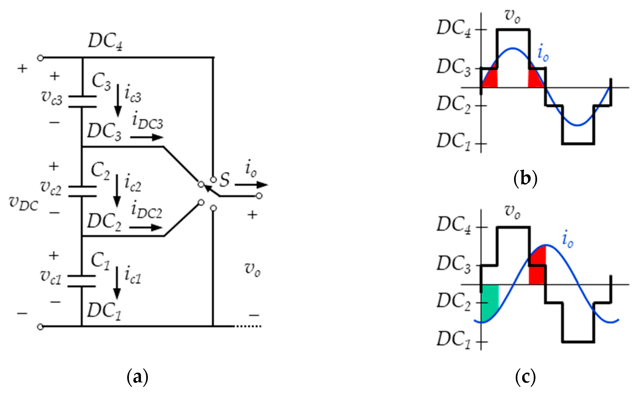
7. Balance in DC–DC Conversion

Although multilevel NPC converters are applied in most cases in DC–AC conversion, there are a small number of applications in DC–DC conversion. Obviously, since the modulations for DC–DC conversion are different from those in DC–AC conversion, the DC-link capacitor voltage balance issue must be addressed in a different manner.
A bidirectional multilevel DC–DC converter implemented with a back-to-back n-level ANPC structure [21] is presented in [79]. The modulation is similar to that of the quasi two-state mode [148], which assures the balance in every switching cycle. However, to guarantee the voltage balance under non-ideal operations, duty ratios are slightly modified by the closed-loop balance control method in [124].
In recent years, interest in the dual active bridge (DAB) converter has grown. The DAB converter features galvanic isolation and bidirectional power transfer capability; thus it is a suitable DC–DC conversion topology for solid state transformers or battery chargers. Moreover, the increasing power levels of these applications can be managed by a multilevel DAB. An illustrative example is found in [163], where a single-phase 3-level NPC DAB is presented. The topology and the switching strategy are shown in Figure 17a,b, respectively. The power flow is regulated by means of the phase shift φ between v a and v b , and the full bridges on each side of the converter have four degrees of freedom.
Two out of the four degrees of freedom affect the capacitor voltage balancing and are reserved for the capacitor voltage balancing control. The remaining two degrees of freedom can be used to optimize the converter performance. Figure 17c shows the proposed control scheme for the capacitor voltage balancing [163]. This control scheme modifies the quarter-wave symmetry switching angles ( α Z 1 , α Z 2 ), obtained considering balanced DC-link voltages, from the imbalance error variable and a compensator. That is, imbalance is corrected by slightly modifying the position of the switching angles to inject or draw current from the DC-link neutral point. This imbalance correction method is applied to single-phase DAB with 3-level [164,165], 4-level [166], n-level [81,167], and three-phase 3-level DAB [168]. A different balancing method is found in [169,170] for a single-phase 3-level DAB, where different switching sequences are applied in each switching period to inject or draw current from the DC-link neutral point, depending on the sign of the DC-link voltage imbalance.

8. Converter Operation beyond Balance

NPC multilevel converters were originally intended for high-voltage and power applications. In this context, DC-link voltage imbalance is not acceptable, since some semiconductor devices have to block an excessive voltage which can lead to a semiconductor failure. However, over the years, the field of application of the NPC multilevel converters has progressively expanded to medium- and low-voltage and power applications, mainly to take advantage of the better waveform quality. Therefore, while working with smaller voltages, the semiconductor devices can bear the different blocking voltages caused by the DC-link voltage imbalance, and the converter is able to operate with this voltage unbalanced condition.
Since unbalanced DC-link capacitor voltages can lead to output voltage distortion, modulations must consider the imbalance to provide undistorted output voltage, as, for instance, for 3-level NPC, carrier-based PWM [171], SVM [172], and VV–SVM [173], among others.
In photovoltaic power systems, the use of multilevel NPC converters, as shown in Figure 18 [32], allows the independent control of the voltage of each photovoltaic array v P V i , such that each photovoltaic array operates at its specific maximum power point. In comparison to a conventional 2-level inverter, this approach is able to maximize the power obtained from the photovoltaic arrays. Although the DC-link capacitor voltages are different to extract the maximum power from each photovoltaic array, with a proper modulation [106], the system in Figure 18 delivers symmetrical and balanced three-phase output currents without low-frequency distortion. A similar implementation is found in [174] and also for a photovoltaic and battery hybrid system [175].
In conventional 2-level inverters with batteries, since the battery modules are series connected, when one of the battery modules is fully discharged, all the series-connected battery modules must stop working to avoid damaging this module. The application of multilevel NPC converters to battery management is shown in Figure 19 [33]. This converter structure allows individual control of the charging/discharging of each battery module. Since the battery modules are not identical, the charges of different battery modules will eventually be different from each other. Therefore, with this individual control, the current of each battery module is controlled to equalize the state of charge of the battery modules. For instance, considering a discharge, all the battery modules are discharged but keeping the same state of charge at all times. Hence, all the battery modules will reach the fully discharged condition at the same time. In comparison to a conventional 2-level system, the system operation can be significantly extended [33].
Finally, DC-link voltage unbalanced operation is also found for a single-phase 4-level NPC inverter [161] and for an asymmetrical DC-link voltage formed by a supercapacitor and a battery [176].

9. Conclusions

This paper presents a review of the state of the art of the control methods of the capacitor voltages in NPC multilevel converters. A summary of these methods is found in Table 1.
A brief description of the converter operation, topologies, and modulations has been presented, prior to the analysis of the capacitor voltage balance issue. The DC-link capacitor voltages are regulated by controlling the DC-link neutral-point currents. This control can be achieved basically by means of a proper selection of the switching states of the converter.
Among the many open-loop modulations to keep the balance, the virtual-vector space-vector modulation is a robust option, since it allows keeping the balance within every switching period, for all operating conditions, although at the cost of a higher number of commutations. However, converter non-idealities can introduce deviations in the open-loop modulation performance and can lead to imbalance. Therefore, the use of a closed-loop balancing method becomes essential in most cases.
The injection of zero-sequence voltage to the open-loop modulation, based on the feedback of the DC-link voltages, is the most usual closed-loop control method. With this strategy, the DC-link neutral-point currents are regulated to adjust the DC-link voltages, both to keep the balance or to set the DC-link capacitor voltages to the desired reference value.
Balance can also be achieved with hardware methods, by means of an external circuitry added to the converter to keep the balance. However, it is preferred to avoid these hardware methods since they introduce higher complexity and cost.
Balance in DC–DC conversion has also been considered, in particular, the multilevel NPC-DAB converter.
Some applications, such as photovoltaic generation, can benefit from working with different DC-link capacitor voltages. This can be implemented with the multilevel NPC converters. In this case, the goal is not to keep the balance but to control each DC-link capacitor voltage to the desired reference value through the proper control of the DC-link neutral-point currents.
Similarly, in battery powered systems, a multilevel NPC converter can enable the independent control of the current of each battery module in a DC-link formed by a series connection of battery modules, with the ultimate goal to achieve an equal state-of-charge of all battery modules. This control is possible, again, through the proper control of the neutral-point currents.
Finally, it is worth highlighting that there are many available options to solve the problem of the balance or regulation of the DC-link capacitor voltages in multilevel NPC converters. At present, since the balance can be assured, the challenge lies more in improving the converter operation by reducing harmonic distortion or increasing efficiency, among others.

Author Contributions

Conceptualization, S.B.-M. and S.A.; introduction, S.A. and S.B.-M.; fundamentals, S.A., S.B.-M., J.B., X.Y. and S.K.; analysis of capacitor voltage balance, S.B.-M., S.A., J.N.-A., À.F.-M., J.B. and S.K.; open-loop techniques, S.B.-M. and S.A.; closed-loop techniques, S.B.-M. and S.A.; hardware methods, S.B.-M. and S.A.; balance in dc-dc conversion, À.F.-M., J.N.-A., S.B.-M. and S.A.; operation beyond balance S.B.-M., J.N.-A., À.F.-M. and S.A.; conclusions, S.A. and S.B.-M.; writing—original draft preparation, S.A. and S.B.-M.; writing—review and editing, S.A., S.B.-M., J.N.-A., À.F.-M., J.B., X.Y. and S.K.; project administration, S.B.-M. and S.A.; funding acquisition, S.B.-M. All authors have read and agreed to the published version of the manuscript.

Funding

This publication is part of Grant DPI2017-89153-P, funded by MCIN/AEI/10.13039/501100011033 and by ERDF A way of making Europe.

Conflicts of Interest

The authors declare no conflict of interest. The funders had no role in the design of the study; in the collection, analyses, or interpretation of data; in the writing of the manuscript, or in the decision to publish the results.

Abbreviations

ANPCActive neutral-point-clamped converter
DABDual active nridge
DPCDirect power control
DTCDirect torque control
FPGAField programmable gate array
MPCModel predictive control
NPCNeutral-point-clamped converter
NTV-SVMNearest-three-vectors SVM
PIProportional-integral controller
PIDProportional-integral-derivative controller
PWMPulse width modulation
SHESelective harmonic elimination
SVMSpace vector modulation
VV-SVMVirtual-vector SVM
3D-SVMThree-dimensional SVM

References

  1. Nabae, A.; Takahashi, I.; Akagi, H. A New Neutral-Point-Clamped PWM Inverter. IEEE Trans. Ind. Appl. 1981, IA-17, 518–523. [Google Scholar] [CrossRef]
  2. Bhagwat, P.M.; Stefanovic, V.R. Generalized Structure of a Multilevel PWM Inverter. IEEE Trans. Ind. Appl. 1983, IA-19, 1057–1069. [Google Scholar] [CrossRef]
  3. Rodriguez, J.; Bernet, S.; Steimer, P.K.; Lizama, I.E. A Survey on Neutral-Point-Clamped Inverters. IEEE Trans. Ind. Electron. 2010, 57, 2219–2230. [Google Scholar] [CrossRef]
  4. Busquets-Monge, S. Neutral-Point-Clamped DC-AC Power Converters. In Wiley Encyclopedia of Electrical and Electronics Engineering; John Wiley & Sons, Inc.: Hoboken, NJ, USA, 2018; pp. 1–20. [Google Scholar]
  5. Choi, N.S.; Cho, J.G.; Cho, G.H. A General Circuit Topology of Multilevel Inverter. In Proceedings of the IEEE Power Electronics Specialists Conference (PESC), Cambridge, MA, USA, 24–27 June 1991; IEEE: Piscataway, NJ, USA, 1991; pp. 96–103. [Google Scholar]
  6. Yuan, X.; Barbi, I. Fundamentals of a new diode clamping multilevel inverter. IEEE Trans. Power Electron. 2000, 15, 711–718. [Google Scholar] [CrossRef]
  7. Abu-Rub, H.; Holtz, J.; Rodriguez, J.; Baoming, G. Medium-Voltage Multilevel Converters—State of the Art, Challenges, and Requirements in Industrial Applications. IEEE Trans. Ind. Electron. 2010, 57, 2581–2596. [Google Scholar] [CrossRef]
  8. Rodriguez, J.; Bernet, S.; Wu, B.; Pontt, J.O.; Kouro, S. Multilevel Voltage-Source-Converter Topologies for Industrial Medium-Voltage Drives. IEEE Trans. Ind. Electron. 2007, 54, 2930–2945. [Google Scholar] [CrossRef]
  9. Rodriguez, J.; Franquelo, L.G.; Kouro, S.; Leon, J.I.; Portillo, R.; Prats, M.A.M.; Perez, M.A. Multilevel Converters: An Enabling Technology for High-Power Applications. Proc. IEEE 2009, 97, 1786–1817. [Google Scholar] [CrossRef] [Green Version]
  10. Leon, J.I.; Vazquez, S.; Franquelo, L.G. Multilevel Converters: Control and Modulation Techniques for Their Operation and Industrial Applications. Proc. IEEE 2017, 105, 2066–2081. [Google Scholar] [CrossRef]
  11. Franquelo, L.G.; Rodriguez, J.; Leon, J.I.; Kouro, S.; Portillo, R.; Prats, M.A.M. The age of multilevel converters arrives. IEEE Ind. Electron. Mag. 2008, 2, 28–39. [Google Scholar] [CrossRef] [Green Version]
  12. Akagi, H. Multilevel Converters: Fundamental Circuits and Systems. Proc. IEEE 2017, 105, 2048–2065. [Google Scholar] [CrossRef]
  13. Rodriguez, J.; Lai, J.-S.; Peng, F.Z. Multilevel inverters: A survey of topologies, controls, and applications. IEEE Trans. Ind. Electron. 2002, 49, 724–738. [Google Scholar] [CrossRef] [Green Version]
  14. Mittal, N.; Singh, B.; Singh, S.; Dixit, R.; Kumar, D. Multilevel inverters: A literature survey on topologies and control strategies. In Proceedings of the 2012 2nd International Conference on Power, Control and Embedded Systems, Allahabad, India, 17–19 December 2012; pp. 1–11. [Google Scholar] [CrossRef]
  15. Sato, Y.; Ito, T. Experimental verification of loss reduction in diode-clamped multilevel inverters. In Proceedings of the 2011 IEEE Energy Conversion Congress and Exposition, Phoenix, AZ, USA, 17–22 September 2011; pp. 190–196. [Google Scholar] [CrossRef]
  16. Lai, J.; Peng, F.Z. Multilevel converters-a new breed of power converters. IEEE Trans. Ind. Appl. 1996, 32, 509–517. [Google Scholar] [CrossRef]
  17. Peng, F.Z. A generalized multilevel inverter topology with self voltage balancing. IEEE Trans. Ind. Appl. 2001, 37, 611–618. [Google Scholar] [CrossRef]
  18. Meynard, T.; Foch, H. Dispositif Électroniquede Conversion d’énergie Électrique 1991. pp. 1–57. Available online: https://patents.google.com/patent/WO1993002501A1/fr (accessed on 10 December 2021).
  19. Debnath, S.; Qin, J.; Bahrani, B.; Saeedifard, M.; Barbosa, P. Operation, Control, and Applications of the Modular Multilevel Converter: A Review. IEEE Trans. Power Electron. 2014, 30, 37–53. [Google Scholar] [CrossRef]
  20. Gateau, G.; Meynard, T.A.; Foch, H. Stacked Multicell Converter (SMC): Properties and Design. In Proceedings of the IEEE Power Electronics Specialists Conference (PESC), Vancouver, BC, Canada, 17–22 September 2001; Volume 3, pp. 1583–1588. [Google Scholar]
  21. Busquets-Monge, S.; Nicolas-Apruzzese, J. A Multilevel Active-Clamped Converter Topology—Operating Principle. IEEE Trans. Ind. Electron. 2010, 58, 3868–3878. [Google Scholar] [CrossRef]
  22. Vemuganti, H.P.; Sreenivasarao, D.; Ganjikunta, S.K.; Suryawanshi, H.M.; Abu-Rub, H. A Survey on Reduced Switch Count Multilevel Inverters. IEEE Open J. Ind. Electron. Soc. 2021, 2, 80–111. [Google Scholar] [CrossRef]
  23. Menzies, R.W.; Steimer, P.; Steinke, J.K. Five Level GTO Inverters for Large Induction Motor Drives. In Proceedings of the IEEE Industry Applications Conference (IAS), 2–8 October 1993; IEEE: Piscataway, NJ, USA; Volume 1, pp. 595–601. [Google Scholar]
  24. Kouro, S.; Malinowski, M.; Gopakumar, K.; Pou, J.; Franquelo, L.G.; Wu, B.; Rodriguez, J.; Perez, M.A.; Leon, J.I. Recent Advances and Industrial Applications of Multilevel Converters. IEEE Trans. Ind. Electron. 2010, 57, 2553–2580. [Google Scholar] [CrossRef]
  25. Welchko, B.A.; de Rossiter Correa, M.B.; Lipo, T.A. A Three-Level MOSFET Inverter for Low-Power Drives. IEEE Trans. Ind. Electron. 2004, 51, 669–674. [Google Scholar] [CrossRef]
  26. Teichmann, R.; Bernet, S. A Comparison of Three-Level Converters Versus Two-Level Converters for Low-Voltage Drives, Traction, and Utility Applications. IEEE Trans. Ind. Appl. 2005, 41, 855–865. [Google Scholar] [CrossRef]
  27. Schweizer, M.; Kolar, J.W. Design and Implementation of a Highly Efficient Three-Level T-Type Converter for Low-Voltage Applications. IEEE Trans. Power Electron. 2012, 28, 899–907. [Google Scholar] [CrossRef]
  28. Daher, S.; Schmid, J.; Antunes, F.L.M. Multilevel Inverter Topologies for Stand-Alone PV Systems. IEEE Trans. Ind. Electron. 2008, 55, 2703–2712. [Google Scholar] [CrossRef]
  29. Bezerra, P.A.M.; Krismer, F.; Kolar, J.W.; Aljameh, R.K.; Paredes, S.; Heller, R.; Brunschwiler, T.; Francese, P.A.; Morf, T.; Kossel, M.A.; et al. Electrical and Thermal Characterization of an Inductor-Based ANPC-Type Buck Converter in 14 nm CMOS Technology for Microprocessor Applications. IEEE Open J. Power Electron. 2020, 1, 456–468. [Google Scholar] [CrossRef]
  30. Marchesoni, M.; Tenca, P. Diode-clamped multilevel converters: A practicable way to balance DC-link voltages. IEEE Trans. Ind. Electron. 2002, 49, 752–765. [Google Scholar] [CrossRef]
  31. Ogasawara, S.; Akagi, H. Analysis of variation of neutral point potential in neutral-point-clamped voltage source PWM inverters. In Proceedings of the Conference Record of the 1993 IEEE Industry Applications Conference Twenty-Eighth IAS Annual Meeting, Toronto, ON, Canada, 2–8 October 1993; IEEE: Piscataway, NJ, USA, 1993; Volume 2, pp. 965–970. [Google Scholar] [CrossRef] [Green Version]
  32. Busquets-Monge, S.; Rocabert, J.; Rodriguez, P.; Alepuz, S.; Bordonau, J. Multilevel Diode-Clamped Converter for Photovoltaic Generators With Independent Voltage Control of Each Solar Array. IEEE Trans. Ind. Electron. 2008, 55, 2713–2723. [Google Scholar] [CrossRef]
  33. Busquets-Monge, S.; Filba-Martinez, A.; Alepuz, S.; Nicolas-Apruzzese, J.; Luque, A.; Roca, A.C.; Bordonau, J. Multibattery-Fed Neutral-Point-Clamped DC–AC Converter With SoC Balancing Control to Maximize Capacity Utilization. IEEE Trans. Ind. Electron. 2019, 67, 16–27. [Google Scholar] [CrossRef]
  34. Nicolas-Apruzzese, J.; Busquets-Monge, S.; Bordonau, J.; Alepuz, S.; Calle-Prado, A.; Filba-Martinez, A. Experimental Effi-ciency Comparison between a Four-Level Active-Clamped and a Two-Level Topology. In Proceedings of the IEEE Industrial Electronics Conference (IECON), Vienna, Austria, 10–14 November 2013; IEEE: Piscataway, NJ, USA, 2013; pp. 6227–6232. [Google Scholar]
  35. Lim, Z.; Maswood, A.I.; Ooi, G.H.P.; Ooi, H.P.G. Common-Mode Reduction for ANPC With Enhanced Harmonic Profile Using Interleaved Sawtooth Carrier Phase-Disposition PWM. IEEE Trans. Ind. Electron. 2016, 63, 7887–7897. [Google Scholar] [CrossRef]
  36. Yaramasu, V.; Wu, B.; Rivera, M.; Narimani, M.; Kouro, S.; Rodriguez, J. Generalised approach for predictive control with common-mode voltage mitigation in multilevel diode-clamped converters. IET Power Electron. 2015, 8, 1440–1450. [Google Scholar] [CrossRef]
  37. Lezana, P.; Pou, J.; Meynard, T.; Rodriguez, J.; Ceballos, S.; Richardeau, F. Survey on Fault Operation on Multilevel Inverters. IEEE Trans. Ind. Electron. 2009, 57, 2207–2218. [Google Scholar] [CrossRef] [Green Version]
  38. Azer, P.; Ounie, S.; Narimani, M. A New Post-Fault Control Method Based on Sinusoidal Pulse Width Modulation Technique for a Neutral Point Clamped (NPC) Inverter. In Proceedings of the IEEE Applied Power Electronics Conference and Exposition (APEC), Anaheim, CA, USA, 17–21 March 2019; pp. 2499–2504. [Google Scholar] [CrossRef]
  39. Bruckner, T.; Bernet, S.; Guldner, H. The Active NPC Converter and Its Loss-Balancing Control. IEEE Trans. Ind. Electron. 2005, 52, 855–868. [Google Scholar] [CrossRef]
  40. Celanovic, N.; Boroyevich, D. A comprehensive study of neutral-point voltage balancing problem in three-level neutral-point-clamped voltage source PWM inverters. IEEE Trans. Power Electron. 2000, 15, 242–249. [Google Scholar] [CrossRef]
  41. Jiang, W.-D.; Du, S.-W.; Chang, L.-C.; Zhang, Y.; Zhao, Q. Hybrid PWM Strategy of SVPWM and VSVPWM for NPC Three-Level Voltage-Source Inverter. IEEE Trans. Power Electron. 2010, 25, 2607–2619. [Google Scholar] [CrossRef]
  42. Hatti, N.; Hasegawa, K.; Akagi, H. A 6.6-kV Transformerless Motor Drive Using a Five-Level Diode-Clamped PWM Inverter for Energy Savings of Pumps and Blowers. IEEE Trans. Power Electron. 2009, 24, 796–803. [Google Scholar] [CrossRef]
  43. Hasegawa, K.; Akagi, H. Low-Modulation-Index Operation of a Five-Level Diode-Clamped PWM Inverter With a DC-Voltage-Balancing Circuit for a Motor Drive. IEEE Trans. Power Electron. 2012, 27, 3495–3504. [Google Scholar] [CrossRef]
  44. Lee, J.-S.; Lee, K.-B. New Modulation Techniques for a Leakage Current Reduction and a Neutral-Point Voltage Balance in Transformerless Photovoltaic Systems Using a Three-Level Inverter. IEEE Trans. Power Electron. 2013, 29, 1720–1732. [Google Scholar] [CrossRef]
  45. Naik, T.; Wandhare, R.G.; Agarwal, V. Three-Level NPC Inverter with Novel Voltage Equalization for PV Grid Interface Suitable for Partially Shaded Conditions. In Proceedings of the IEEE Power and Energy Conference at Illinois (PECI), Urbana, IL, USA, 22–23 February 2013; pp. 186–193. [Google Scholar]
  46. Alepuz, S.; Busquets-Monge, S.; Bordonau, J.; Gago, J.; Gonzalez, D.; Balcells, J. Interfacing Renewable Energy Sources to the Utility Grid Using a Three-Level Inverter. IEEE Trans. Ind. Electron. 2006, 53, 1504–1511. [Google Scholar] [CrossRef]
  47. Yaramasu, V.; Wu, B.; Rivera, M.; Rodriguez, J. A New Power Conversion System for Megawatt PMSG Wind Turbines Using Four-Level Converters and a Simple Control Scheme Based on Two-Step Model Predictive Strategy—Part I: Modeling and Theoretical Analysis. IEEE J. Emerg. Sel. Top. Power Electron. 2013, 2, 3–13. [Google Scholar] [CrossRef]
  48. Yaramasu, V.; Wu, B.; Rivera, M.; Rodriguez, J. A New Power Conversion System for Megawatt PMSG Wind Turbines Using Four-Level Converters and a Simple Control Scheme Based on Two-Step Model Predictive Strategy—Part II: Simulation and Experimental Analysis. IEEE J. Emerg. Sel. Top. Power Electron. 2013, 2, 14–25. [Google Scholar] [CrossRef]
  49. Faulstich, A.; Steinke, J.K.; Wittwer, F. Medium Voltage Converter for Permanent Magnet Wind Power Generators up to 5 MW. In Proceedings of the European Conference on Power Electronics and Applications (EPE), Dresden, Germany, 11–14 September 2005; IEEE: Piscataway, NJ, USA, 2005; pp. 1–9. [Google Scholar]
  50. Shu, Z.; Ding, N.; Chen, J.; Zhu, H.; He, X. Multilevel SVPWM With DC-Link Capacitor Voltage Balancing Control for Diode-Clamped Multilevel Converter Based STATCOM. IEEE Trans. Ind. Electron. 2012, 60, 1884–1896. [Google Scholar] [CrossRef]
  51. Friedemann, R.A.; Krismer, F.; Kolar, J.W. Design of a minimum weight dual active bridge converter for an Airborne Wind Turbine system. In Proceedings of the 2012 Twenty-Seventh Annual IEEE Applied Power Electronics Conference and Exposition (APEC), Orlando, FL, USA, 5–9 February 2012; pp. 509–516. [Google Scholar] [CrossRef]
  52. Yuan, X. Derivation of Voltage Source Multilevel Converter Topologies. IEEE Trans. Ind. Electron. 2016, 64, 966–976. [Google Scholar] [CrossRef] [Green Version]
  53. Bruckner, T.; Bemet, S. Loss Balancing in Three-Level Voltage Source Inverters Applying Active NPC Switches. In Proceedings of the IEEE Power Electronics Specialists Conference (PESC), Vancouver, BC, Canada, 17–21 June 2001; IEEE: Piscataway, NJ, USA, 2001; Volume 2, pp. 1135–1140. [Google Scholar]
  54. Brückner, T.; Bernet, S.; Steimer, P.K. Feedforward Loss Control of Three-Level Active NPC Converters. IEEE Trans. Ind. Appl. 2007, 43, 1588–1596. [Google Scholar] [CrossRef]
  55. Dixon, J.; Moran, L. High-level multistep inverter optimization using a minimum number of power transistors. IEEE Trans. Power Electron. 2006, 21, 330–337. [Google Scholar] [CrossRef]
  56. Wang, J.; Yuan, X.; Dagan, K.J.; Bloor, A. Optimal Neutral Point Voltage Balancing Algorithm for Three-phase Three-level Converters with Hybrid Zero-sequence Signal Injection and Virtual Zero-level Modulation. IEEE Trans. Ind. Appl. 2020, 56, 1. [Google Scholar] [CrossRef]
  57. Wang, J.; Yuan, X.; Jin, B.; Laird, I. Closed-Loop DC-Link Voltage Balancing Algorithm for a Four-Level π-Type Converter. In Proceedings of the IEEE Industrial Electronics Conference (IECON), Lisbon, Portugal, 1 October 2019; pp. 3529–3534. [Google Scholar]
  58. Jin, B.; Yuan, X. Topology, Efficiency Analysis, and Control of a Four-Level $\pi$ -Type Converter. IEEE J. Emerg. Sel. Top. Power Electron. 2018, 7, 1044–1059. [Google Scholar] [CrossRef]
  59. Rodriguez, J.; Moran, L.; Correa, P.; Silva, C. A vector control technique for medium-voltage multilevel inverters. IEEE Trans. Ind. Electron. 2002, 49, 882–888. [Google Scholar] [CrossRef]
  60. Dahidah, M.S.A.; Konstantinou, G.; Agelidis, V.G. A Review of Multilevel Selective Harmonic Elimination PWM: Formulations, Solving Algorithms, Implementation and Applications. IEEE Trans. Power Electron. 2014, 30, 4091–4106. [Google Scholar] [CrossRef]
  61. Leon, J.I.; Kouro, S.; Franquelo, L.G.; Rodriguez, J.; Wu, B. The Essential Role and the Continuous Evolution of Modulation Techniques for Voltage-Source Inverters in the Past, Present, and Future Power Electronics. IEEE Trans. Ind. Electron. 2016, 63, 2688–2701. [Google Scholar] [CrossRef]
  62. McGrath, B.; Holmes, D. Multicarrier PWM strategies for multilevel inverters. IEEE Trans. Ind. Electron. 2002, 49, 858–867. [Google Scholar] [CrossRef]
  63. Carrara, G.; Gardella, S.; Marchesoni, M.; Salutari, R.; Sciutto, G. A new multilevel PWM method: A theoretical analysis. IEEE Trans. Power Electron. 1992, 7, 497–505. [Google Scholar] [CrossRef]
  64. van der Broeck, H.; Skudelny, H.-C.; Stanke, G. Analysis and realization of a pulsewidth modulator based on voltage space vectors. IEEE Trans. Ind. Appl. 1988, 24, 142–150. [Google Scholar] [CrossRef]
  65. Holmes, D.G.; Lipo, T.A. Pulse Width Modulation for Power Converters-Principles and Practice; IEEE Press-John Wiley & Sons: Piscataway, NJ, USA, 2003. [Google Scholar]
  66. Celanovic, N.; Boroyevich, D. A fast space-vector modulation algorithm for multilevel three-phase converters. IEEE Trans. Ind. Appl. 2001, 37, 637–641. [Google Scholar] [CrossRef]
  67. Seo, J.H.; Choi, C.H.; Hyun, D.-S. A new simplified space-vector PWM method for three-level inverters. IEEE Trans. Power Electron. 2001, 16, 545–550. [Google Scholar] [CrossRef]
  68. Tan, Z.; Li, Y.; Li, M. A Direct Torque Control of Induction Motor Based on Three-Level NPC Inverter. In Proceedings of the IEEE Power Electronics Specialists Conference (PESC), Vancouver, BC, Canada, 17–21 June 2001; Volume 3, pp. 1435–1439. [Google Scholar]
  69. Busquets-Monge, S.; Bordonau, J.; Boroyevich, D.; Somavilla, S. The nearest three virtual space vector PWM - A modulation for the comprehensive neutral-point balancing in the three-level NPC inverter. IEEE Power Electron. Lett. 2004, 2, 11–15. [Google Scholar] [CrossRef]
  70. Gui, S.W.; Lin, Z.J.; Huang, S.H. A Varied VSVM Strategy for Balancing the Neutral-Point Voltage of DC-Link Capacitors in Three-Level NPC Converters. Energies 2015, 8, 2032–2047. [Google Scholar] [CrossRef] [Green Version]
  71. Prats, M.; Franquelo, L.G.; Portillo, R.; Leon, J.I.; Galvan, E.; Carrasco, J. A 3-D space vector modulation generalized algorithm for multilevel converters. IEEE Power Electron. Lett. 2003, 1, 110–114. [Google Scholar] [CrossRef]
  72. Franquelo, L.; Prats, M.; Portillo, R.; Galvan, J.; Perales, M.; Carrasco, J.; Diez, E.; Jimenez, J. Three-dimensional space-vector modulation algorithm for four-leg multilevel converters using abc coordinates. IEEE Trans. Ind. Electron. 2006, 53, 458–466. [Google Scholar] [CrossRef]
  73. Holmes, D. The general relationship between regular-sampled pulse-width-modulation and space vector modulation for hard switched converters. In Proceedings of the Conference Record of the 1992 IEEE Industry Applications Society Annual Meeting, Houston, TX, USA, 4–9 October 1992; Volume 1, pp. 1002–1009. [Google Scholar] [CrossRef]
  74. Bowes, S.; Lai, Y.-S. The relationship between space-vector modulation and regular-sampled PWM. IEEE Trans. Ind. Electron. 1997, 44, 670–679. [Google Scholar] [CrossRef]
  75. Zhou, K.; Wang, D. Relationship between space-vector modulation and three-phase carrier-based PWM: A comprehensive analysis [three-phase inverters]. IEEE Trans. Ind. Electron. 2002, 49, 186–196. [Google Scholar] [CrossRef]
  76. Wang, F. Sine-triangle versus space-vector modulation for three-level PWM voltage-source inverters. IEEE Trans. Ind. Appl. 2002, 38, 500–506. [Google Scholar] [CrossRef]
  77. Chen, J.; He, Y.; Hasan, S.U.; Liu, J. A Comprehensive Study on Equivalent Modulation Waveforms of the SVM Sequence for Three-Level Inverters. IEEE Trans. Power Electron. 2015, 30, 7149–7158. [Google Scholar] [CrossRef]
  78. Sourkounis, C.; Al-Diab, A. A comprehensive analysis and comparison between Multilevel Space-Vector Modulation and Multilevel Carrier-Based PWM. In Proceedings of the 2008 13th International Power Electronics and Motion Control Conference, Poznan, Poland, 1–3 September 2008; pp. 1710–1715. [Google Scholar] [CrossRef]
  79. Busquets-Monge, S.; Alepuz, S.; Bordonau, J. A novel bidirectional multilevel boost-buck dc-dc Convert. In Proceedings of the 2009 IEEE Energy Conversion Congress and Exposition, San Jose, CA, USA, 20–24 September 2009; pp. 707–714. [Google Scholar] [CrossRef] [Green Version]
  80. Liu, P.; Chen, C.; Duan, S.; Zhu, W. Dual Phase-Shifted Modulation Strategy for the Three-Level Dual Active Bridge DC–DC Converter. IEEE Trans. Ind. Electron. 2017, 64, 7819–7830. [Google Scholar] [CrossRef]
  81. Filba-Martinez, A.; Busquets-Monge, S.; Bordonau, J. Modulation and Capacitor Voltage Balancing Control of Multilevel NPC Dual Active Bridge DC–DC Converters. IEEE Trans. Ind. Electron. 2019, 67, 2499–2510. [Google Scholar] [CrossRef]
  82. Sapin, A.; Steimer, P.K.; Simond, J.-J. Modeling, Simulation, and Test of a Three-Level Voltage-Source Inverter With Output $LC$ Filter and Direct Torque Control. IEEE Trans. Ind. Appl. 2007, 43, 469–475. [Google Scholar] [CrossRef]
  83. Rivera, S.; Kouro, S.; Wu, B.; Alepuz, S.; Malinowski, M.; Cortes, P.; Rodriguez, J. Multilevel Direct Power Control—A Generalized Approach for Grid-Tied Multilevel Converter Applications. IEEE Trans. Power Electron. 2013, 29, 5592–5604. [Google Scholar] [CrossRef]
  84. Vargas, R.; Cortes, P.; Ammann, U.; Rodriguez, J.; Pontt, J. Predictive Control of a Three-Phase Neutral-Point-Clamped Inverter. IEEE Trans. Ind. Electron. 2007, 54, 2697–2705. [Google Scholar] [CrossRef]
  85. Martins, C.; Roboam, X.; Meynard, T.; Carvalho, A. Switching frequency imposition and ripple reduction in DTC drives by using a multilevel converter. IEEE Trans. Power Electron. 2002, 17, 286–297. [Google Scholar] [CrossRef]
  86. Cortes, P.; Rodriguez, J.; Quevedo, D.E.; Silva, C. Predictive Current Control Strategy With Imposed Load Current Spectrum. IEEE Trans. Power Electron. 2008, 23, 612–618. [Google Scholar] [CrossRef]
  87. Verne, S.A.; Gonzalez, S.A.; Valla, M.I. An optimization algorithm for capacitor voltage balance of N-level Diode Clamped Inverters. In Proceedings of the 2008 34th Annual Conference of IEEE Industrial Electronics, Orlando, FL, USA, 10–13 November 2008; pp. 3201–3206. [Google Scholar] [CrossRef]
  88. Steinke, J. Switching frequency optimal PWM control of a three-level inverter. IEEE Trans. Power Electron. 1992, 7, 487–496. [Google Scholar] [CrossRef]
  89. Wang, K.; Zheng, Z.; Xu, L.; Li, Y. A Generalized Carrier-Overlapped PWM Method for Neutral-Point-Clamped Multilevel Converters. IEEE Trans. Power Electron. 2020, 35, 9095–9106. [Google Scholar] [CrossRef]
  90. Busquets-Monge, S.; Bordonau, J.; Rocabert, J. A Virtual-Vector Pulsewidth Modulation for theFour-Level Diode-Clamped DC–AC Converter. IEEE Trans. Power Electron. 2008, 23, 1964–1972. [Google Scholar] [CrossRef]
  91. Imarazene, K.; Chekireb, H.; Berkouk, E.M. Balancing DC Link Using the Redundant States Method in Selective Harmonics Elimination PWM. In Proceedings of the International Symposium on Advanced Electromechanical Motion Systems and Electric Drives (ELECTROMOTION), Lillie, France, 1–3 July 2009. [Google Scholar]
  92. Wu, M.; Li, Y.W.; Konstantinou, G. A Comprehensive Review of Capacitor Voltage Balancing Strategies for Multilevel Converters Under Selective Harmonic Elimination PWM. IEEE Trans. Power Electron. 2020, 36, 2748–2767. [Google Scholar] [CrossRef]
  93. Pan, Z.; Peng, F.Z.; Corzine, K.; Stefanovic, V.; Leuthen, J.; Gataric, S. Voltage Balancing Control of Diode-Clamped Multilevel Rectifier/Inverter Systems. IEEE Trans. Ind. Appl. 2005, 41, 1698–1706. [Google Scholar] [CrossRef]
  94. Celanovic, N.; Celanovic, I.; Boroyevich, D. The feedforward method of controlling three-level diode clamped converters with small DC-link capacitors. In Proceedings of the 2001 IEEE 32nd Annual Power Electronics Specialists Conference, Vancouver, BC, Canada, 17–21 June 2001; Volume 3, pp. 1357–1362. [Google Scholar] [CrossRef]
  95. Seo, J.H.; Choi, C.H. Compensation for the Neutral-Point Potential Variation in Three-Level Space Vector PWM. In Proceedings of the IEEE Applied Power Electronics Conference and Exposition (APEC), Anaheim, CA, USA, 4–8 March 2001; Volume 2, pp. 1135–1140. [Google Scholar]
  96. Mouton, H.D.T. Natural balancing of three-level neutral-point-clamped PWM inverters. IEEE Trans. Ind. Electron. 2002, 49, 1017–1025. [Google Scholar] [CrossRef]
  97. Stala, R. A Natural DC-Link Voltage Balancing of Diode-Clamped Inverters in Parallel Systems. IEEE Trans. Ind. Electron. 2012, 60, 5008–5018. [Google Scholar] [CrossRef]
  98. Shen, J.; Schröder, S.; Rösner, R.; Elbarbari, S.F.S. A Comprehensive Study of Neutral-Point Self-Balancing Effect in Neutral-Point-Clamped Three-Level Inverters. IEEE Trans. Power Electron. 2011, 26, 3084–3095. [Google Scholar] [CrossRef]
  99. Newton, C.; Sumner, M. Neutral Point Control for Multi-Level Inverters: Theory, Design and Operational Limitations. In Proceedings of the IEEE Industry Applications Conference (IAS), New Orleans, LA, USA, 5–9 October 1997; pp. 1336–1343. [Google Scholar]
  100. Fracchia, M.; Ghiara, T.; Marchesoni, M.; Mazzucchelli, M. Optimized Modulation Techniques for the Generalized N-Level Converter. In Proceedings of the IEEE Power Electronics Specialists Conference (PESC), Toledo, Spain, 29 June–3 July 1992; Institute of Electrical and Electronics Engineers Inc.: Manhattan, NY, USA; pp. 1205–1213. [Google Scholar]
  101. Marchesoni, M.; Tenca, P. Theoretical and Practical Limits in Multilevel MPC Inverters with Passive Front Ends. In Proceedings of the European Conference on Power Electronics and Applications (EPE), Graz, Austria, 22–24 June 2001; pp. 1–10. [Google Scholar]
  102. Busquets-Monge, S.; Ortega, J.D.; Bordonau, J.; Beristain, J.A.; Rocabert, J. Closed-Loop Control of a Three-Phase Neutral-Point-Clamped Inverter Using an Optimized Virtual-Vector-Based Pulsewidth Modulation. IEEE Trans. Ind. Electron. 2008, 55, 2061–2071. [Google Scholar] [CrossRef]
  103. Lee, D.H.; Lee, S.R.; Lee, F.C. An Analysis of Midpoint Balance for the Neutral-Point-Clamped Three-Level VSI. In Proceedings of the IEEE Power Electronics Specialists Conference (PESC), Fukuoka, Japan, 22–22 May 1998; Volume 1, pp. 193–199. [Google Scholar]
  104. Pou, J.; Pindado, R.; Boroyevich, D.; Rodriguez, P. Evaluation of the Low-Frequency Neutral-Point Voltage Oscillations in the Three-Level Inverter. IEEE Trans. Ind. Electron. 2005, 52, 1582–1588. [Google Scholar] [CrossRef]
  105. Wang, C.; Li, Y. Analysis and Calculation of Zero-Sequence Voltage Considering Neutral-Point Potential Balancing in Three-Level NPC Converters. IEEE Trans. Ind. Electron. 2009, 57, 2262–2271. [Google Scholar] [CrossRef]
  106. Busquets-Monge, S.; Alepuz, S.; Rocabert, J.; Bordonau, J. Pulsewidth Modulations for the Comprehensive Capacitor Voltage Balance of $n$-Level Three-Leg Diode-Clamped Converters. IEEE Trans. Power Electron. 2009, 24, 1364–1375. [Google Scholar] [CrossRef] [Green Version]
  107. Busquets-Monge, S.; Alepuz, S.; Rocabert, J.; Bordonau, J. Pulsewidth Modulations for the Comprehensive Capacitor Voltage Balance of $n$-Level Two-Leg Diode-Clamped Converters. IEEE Trans. Power Electron. 2009, 24, 1951–1959. [Google Scholar] [CrossRef]
  108. Monge, S.B.; Somavilla, S.; Bordonau, J.; Boroyevich, D. Capacitor Voltage Balance for the Neutral-Point- Clamped Converter using the Virtual Space Vector Concept With Optimized Spectral Performance. IEEE Trans. Power Electron. 2007, 22, 1128–1135. [Google Scholar] [CrossRef]
  109. Busquets-Monge, S.; Ruderman, A. Carrier-Based PWM Strategies for the Comprehensive Capacitor Voltage Balance of Mul-tilevel Multileg Diode-Clamped Converters. In Proceedings of the IEEE International Symposium on Industrial Electronics (ISIE), Bari, Italy, 4–7 July 2010; pp. 688–693. [Google Scholar]
  110. Busquets-Monge, S.; Maheshwari, R.; Munk-Nielsen, S. Overmodulation of $n$-Level Three-Leg DC–AC Diode-Clamped Converters With Comprehensive Capacitor Voltage Balance. IEEE Trans. Ind. Electron. 2012, 60, 1872–1883. [Google Scholar] [CrossRef]
  111. Maheshwari, R.; Munk-Nielsen, S.; Busquets-Monge, S. A carrier-based approach for overmodulation of three-level neutral-point-clamped inverter with zero neutral-point current. In Proceedings of the 2012 IEEE Energy Conversion Congress and Exposition (ECCE), Raleigh, NC, USA, 15–20 September 2012. [Google Scholar] [CrossRef]
  112. Busquets-Monge, S.; Bordonau, J.; Beristáin, J.A. Comparison of Losses and Thermal Performance of a Three-Level Three-Phase Neutral-Point-Clamped Dc-Ac Converter under a Conventional NTV and the NTV 2 Modulation Strategies. In Proceedings of the IEEE Industrial Electronics Conference (IECON), Paris, France, 6–10 November 2006; pp. 4819–4824. [Google Scholar]
  113. Wang, K.; Zheng, Z.; Li, Y. A Novel Carrier-Overlapped PWM Method for Four-Level Neutral-Point Clamped Converters. IEEE Trans. Power Electron. 2018, 34, 7–12. [Google Scholar] [CrossRef]
  114. Wang, K.; Zheng, Z.; Xu, L.; Li, Y. Neutral-Point Voltage Balancing Method for Five-Level NPC Inverters Based on Carrier-Overlapped PWM. IEEE Trans. Power Electron. 2020, 36, 1428–1440. [Google Scholar] [CrossRef]
  115. Xia, C.; Shao, H.; Zhang, Y.; He, X. Adjustable Proportional Hybrid SVPWM Strategy for Neutral-Point-Clamped Three-Level Inverters. IEEE Trans. Ind. Electron. 2012, 60, 4234–4242. [Google Scholar] [CrossRef]
  116. Fazio, P.; Maragliano, G.; Marchesoni, M.; Vaccaro, L. A New Capacitor Balancing Technique in Diode-Clamped Multilevel Converters with Active Front End for Extended Operation Range. In Proceedings of the European Conference on Power Electronics and Applications (EPE), Birmingham, UK, 30 August–1 September 2011; pp. 1–10. [Google Scholar]
  117. Pou, J.; Boroyevich, D.; Pindado, R. New feedforward space-vector PWM method to obtain balanced AC output voltages in a three-level neutral-point-clamped converter. IEEE Trans. Ind. Electron. 2002, 49, 1026–1034. [Google Scholar] [CrossRef]
  118. Li, Y.; Gao, Y.; Hou, X. A general SVM Algorithm for Multilevel Converters Considering Zero-Sequence Component Control. In Proceedings of the IEEE Industrial Electronics Conference (IECON), Raleigh, NC, USA, 6–10 November 2005; Volume 2005, pp. 508–513. [Google Scholar]
  119. Wang, J.; Wang, J.; Xiao, B.; Gui, Z.; Jiang, W. Full Range Capacitor Voltage Balance PWM Strategy for Diode-Clamped Multilevel Inverter. Electronics 2020, 9, 1263. [Google Scholar] [CrossRef]
  120. Pou, J.; Zaragoza, J.; Ceballos, S.; Saeedifard, M.; Boroyevich, D. A Carrier-Based PWM Strategy With Zero-Sequence Voltage Injection for a Three-Level Neutral-Point-Clamped Converter. IEEE Trans. Power Electron. 2010, 27, 642–651. [Google Scholar] [CrossRef]
  121. Shen, J.; Schroder, S.; Duro, B.; Roesner, R. A Neutral-Point Balancing Controller for a Three-Level Inverter With Full Power-Factor Range and Low Distortion. IEEE Trans. Ind. Appl. 2012, 49, 138–148. [Google Scholar] [CrossRef]
  122. Kim, J.-S.; Kwon, J.-M. Direct Space Vector Modulation with Novel DC-link Voltage Balancing Algorithm for Easy Software Implementation of Three-Phase Three-Level Converter. Electronics 2020, 9, 1841. [Google Scholar] [CrossRef]
  123. Qamar, M.A.; Wang, K.; Zheng, Z.; Wang, S.; Li, Y. A Simplified Virtual Vector PWM Algorithm to Balance the Capacitor Voltages of Four-Level Diode-Clamped Converter. IEEE Access 2020, 8, 180896–180908. [Google Scholar] [CrossRef]
  124. Busquets-Monge, S.; Alepuz, S.; Bordonau, J.; Peracaula, J. Voltage Balancing Control of Diode-Clamped Multilevel Converters With Passive Front-Ends. IEEE Trans. Power Electron. 2008, 23, 1751–1758. [Google Scholar] [CrossRef]
  125. Xiang, C.-Q.; Shu, C.; Han, D.; Mao, B.-K.; Wu, X.; Yu, T.-J. Improved Virtual Space Vector Modulation for Three-Level Neutral-Point-Clamped Converter With Feedback of Neutral-Point Voltage. IEEE Trans. Power Electron. 2017, 33, 5452–5464. [Google Scholar] [CrossRef]
  126. Xia, S.; Wu, X.; Zheng, J.; Li, X.; Wang, K. A Virtual Space Vector PWM With Active Neutral Point Voltage Control and Common Mode Voltage Suppression for Three-Level NPC Converters. IEEE Trans. Ind. Electron. 2021, 68, 11761–11771. [Google Scholar] [CrossRef]
  127. Jiang, W.; Wang, P.; Ma, M.; Wang, J.; Li, J.; Li, L.; Chen, K.; Weidong, J. A Novel Virtual Space Vector Modulation With Reduced Common-Mode Voltage and Eliminated Neutral Point Voltage Oscillation for Neutral Point Clamped Three-Level Inverter. IEEE Trans. Ind. Electron. 2019, 67, 884–894. [Google Scholar] [CrossRef]
  128. Hu, C.; Yu, X.; Holmes, D.G.; Shen, W.; Wang, Q.; Luo, F.; Liu, N. An Improved Virtual Space Vector Modulation Scheme for Three-Level Active Neutral-Point-Clamped Inverter. IEEE Trans. Power Electron. 2016, 32, 7419–7434. [Google Scholar] [CrossRef]
  129. Li, C.; Yang, T.; Kulsangcharoen, P.; Calzo, G.L.; Bozhko, S.; Gerada, C.; Wheeler, P.; Gerada, C. A Modified Neutral Point Balancing Space Vector Modulation for Three-Level Neutral Point Clamped Converters in High-Speed Drives. IEEE Trans. Ind. Electron. 2018, 66, 910–921. [Google Scholar] [CrossRef]
  130. Guo, F.; Yang, T.; Diab, A.M.; Yeoh, S.S.; Bozhko, S.; Wheeler, P. An Enhanced Virtual Space Vector Modulation Scheme of Three-Level NPC Converters for More-Electric-Aircraft Applications. IEEE Trans. Ind. Appl. 2021, 57, 5239–5251. [Google Scholar] [CrossRef]
  131. Maheshwari, R.; Munk-Nielsen, S.; Busquets-Monge, S. Design of Neutral-Point Voltage Controller of a Three-Level NPC Inverter With Small DC-Link Capacitors. IEEE Trans. Ind. Electron. 2012, 60, 1861–1871. [Google Scholar] [CrossRef]
  132. Busquets-Monge, S.; Maheshwari, R.; Nicolas-Apruzzese, J.; Lupon, E.J.; Munk-Nielsen, S.; Bordonau, J. Enhanced DC-Link Capacitor Voltage Balancing Control of DC–AC Multilevel Multileg Converters. IEEE Trans. Ind. Electron. 2014, 62, 2663–2672. [Google Scholar] [CrossRef]
  133. Busquets-Monge, S.; Grino, R.; Nicolas-Apruzzese, J.; Bordonau, J. Decoupled DC-Link Capacitor Voltage Control of DC–AC Multilevel Multileg Converters. IEEE Trans. Ind. Electron. 2015, 63, 1344–1349. [Google Scholar] [CrossRef] [Green Version]
  134. Nicolas-Apruzzese, J.; Lupon, E.; Busquets-Monge, S.; Conesa, A.; Bordonau, J.; García-Rojas, G. FPGA-Based Controller for a Permanent-Magnet Synchronous Motor Drive Based on a Four-Level Active-Clamped DC-AC Converter. Energies 2018, 11, 2639. [Google Scholar] [CrossRef] [Green Version]
  135. Wang, J.; Yuan, X.; Jin, B. Carrier-based Closed-loop DC-link Voltage Balancing Algorithm for Four Level NPC Converters Based on Redundant Level Modulation. IEEE Trans. Ind. Electron. 2020, 68, 11707–11718. [Google Scholar] [CrossRef]
  136. Giri, S.K.; Mukherjee, S.; Kundu, S.; Banerjee, S.; Chakraborty, C. An Improved PWM Scheme for Three-Level Inverter Extending Operation Into Overmodulation Region With Neutral-Point Voltage Balancing for Full Power-Factor Range. IEEE J. Emerg. Sel. Top. Power Electron. 2017, 6, 1527–1539. [Google Scholar] [CrossRef]
  137. Imarazene, K.; Chekireb, H.; Berkouk, E.M. Redundant States in Five-Level Inverter Using Selective Harmonics Elimination PWM. In Proceedings of the International Symposium on Power Electronics, Electrical Drives, Automation and Motion (SPEEDAM), Pisa, Italy, 14–16 June 2010; IEEE Computer Society: Piscataway, NJ, USA, 2010; pp. 198–203. [Google Scholar]
  138. Pulikanti, S.R.; Dahidah, M.S.A.; Agelidis, V.G. Voltage Balancing Control of Three-Level Active NPC Converter Using SHE-PWM. IEEE Trans. Power Deliv. 2010, 26, 258–267. [Google Scholar] [CrossRef]
  139. Busquets-Monge, S.; Filba-Martinez, A.; Alepuz, S.; Calle-Prado, A. A Modulation Strategy to Operate Multilevel Multiphase Diode-Clamped and Active-Clamped DC–AC Converters at Low Frequency Modulation Indices With DC-Link Capacitor Voltage Balance. IEEE Trans. Power Electron. 2016, 32, 7521–7533. [Google Scholar] [CrossRef]
  140. Rojas, R.; Ohnishi, T.; Suzuki, T. Method for Neutral-Point-Clamped Inverters. IEEE Trans. Power Electron. 1995, 10, 666–672. [Google Scholar] [CrossRef]
  141. Wang, J.; Zhang, W.; Ma, M.; Zhang, Q.; Jiang, W. Discontinuous PWM Strategy for Neutral Point Clamped Three-Level Inverter to Achieve Multiple Control Objectives. IEEE Access 2019, 7, 158533–158544. [Google Scholar] [CrossRef]
  142. Yaramasu, V.; Wu, B. Predictive Control of a Three-Level Boost Converter and an NPC Inverter for High-Power PMSG-Based Medium Voltage Wind Energy Conversion Systems. IEEE Trans. Power Electron. 2013, 29, 5308–5322. [Google Scholar] [CrossRef]
  143. Barros, J.; Rocha, L.; Silva, J. Backstepping Predictive Control of Hybrid Microgrids Interconnected by Neutral Point Clamped Converters. Electronics 2021, 10, 1210. [Google Scholar] [CrossRef]
  144. Calle-Prado, A.; Alepuz, S.; Bordonau, J.; Cortes, P.; Rodriguez, J. Predictive Control of a Back-to-Back NPC Converter-Based Wind Power System. IEEE Trans. Ind. Electron. 2016, 63, 4615–4627. [Google Scholar] [CrossRef] [Green Version]
  145. Yaramasu, V.; Wu, B.; Chen, J. Model-Predictive Control of Grid-Tied Four-Level Diode-Clamped Inverters for High-Power Wind Energy Conversion Systems. IEEE Trans. Power Electron. 2013, 29, 2861–2873. [Google Scholar] [CrossRef]
  146. Verne, S.A.; Valla, M.I. Predictive Control of a Back to Back Diode Clamped Multilevel Converter. In Proceedings of the IEEE International Conference on Industrial Technology (ICIT), 14–17 March 2010; IEEE: Piscataway, NJ, USA; pp. 1814–1819. [Google Scholar]
  147. Salem, A.; Mamdouh, M.; Abido, M.A. Capacitor Balancing and Common-Mode Voltage Reduction of a SiC Based Dual T-Type Drive System Using Model Predictive Control. IEEE Access 2019, 7, 41066–41077. [Google Scholar] [CrossRef]
  148. Adam, G.P.; Finney, S.J.; Massoud, A.M.; Williams, B.W. Capacitor Balance Issues of the Diode-Clamped Multilevel Inverter Operated in a Quasi Two-State Mode. IEEE Trans. Ind. Electron. 2008, 55, 3088–3099. [Google Scholar] [CrossRef]
  149. Kang, K.-P.; Cho, Y.; Kim, H.-S.; Baek, J.-W. DC-Link Capacitor Voltage Imbalance Compensation Method Based Injecting Harmonic Voltage for Cascaded Multi-Module Neutral Point Clamped Inverter. Electronics 2019, 8, 155. [Google Scholar] [CrossRef] [Green Version]
  150. Wang, K.; Zheng, Z.; Li, Y.; Xu, L.; Ma, H. Multi-Objective Optimization PWM Control for a Back-to-Back Five-Level ANPC Converter. In Proceedings of the IEEE Energy Conversion Congress and Exposition (ECCE), Raleigh, NC, USA, 15–20 September 2012; pp. 3514–3519. [Google Scholar]
  151. Xu, X.; Zheng, Z.; Wang, K.; Yang, B.; Li, Y. A Comprehensive Study of Common Mode Voltage Reduction and Neutral Point Potential Balance for a Back-to-Back Three-Level NPC Converter. IEEE Trans. Power Electron. 2019, 35, 7910–7920. [Google Scholar] [CrossRef]
  152. Newton, C.; Sumner, M. A Novel Arrangement for Balancing the Capacitor Voltages of a Five Level Diode Clamped Inverter. In Proceedings of the IEE International Conference on Power Electronics and Variable Speed Drives, 21–23 September 1998; IEEE: Piscataway, NJ, USA; pp. 465–470. [Google Scholar]
  153. Lim, S.K.; Kim, J.H.; Nam, K. DC-Link Voltage Balancing Algorithm for 3-Level Converter Using the Zero Sequence Current. In Proceedings of the IEEE Power Electronics Specialists Conference (PESC), Charleston, SC, USA, 1 July 1999; Volume 2, pp. 1083–1088. [Google Scholar]
  154. León, J.I.; Franquelo, L.G.; Portillo, R.C.; Prats, M.M. DC-Link Capacitors Voltage Balancing in Multilevel Four-Leg Di-ode-Clamped Converters. In Proceedings of the IEEE Industrial Electronics Conference (IECON), Raleigh, NC, USA, 6–10 November 2005; Volume 2005, pp. 1254–1259. [Google Scholar]
  155. Ceballos, S.; Pou, J.; Robles, E.; Gabiola, I.; Zaragoza, J.; Villate, J.L.; Boroyevich, D. Three-Level Converter Topologies With Switch Breakdown Fault-Tolerance Capability. IEEE Trans. Ind. Electron. 2008, 55, 982–995. [Google Scholar] [CrossRef]
  156. Shukla, A.; Ghosh, A.; Joshi, A. Flying-Capacitor-Based Chopper Circuit for DC Capacitor Voltage Balancing in Diode-Clamped Multilevel Inverter. IEEE Trans. Ind. Electron. 2009, 57, 2249–2261. [Google Scholar] [CrossRef] [Green Version]
  157. Shu, Z.; He, X.; Wang, Z.; Qiu, D.; Jing, Y. Voltage Balancing Approaches for Diode-Clamped Multilevel Converters Using Auxiliary Capacitor-Based Circuits. IEEE Trans. Power Electron. 2012, 28, 2111–2124. [Google Scholar] [CrossRef]
  158. Corzine, K.A.; Ieee, M. Analysis of a Four-Level DC/DC Buck Converter Department of Electrical Engineering. Electr. Eng. 2001, 1882–1888. [Google Scholar]
  159. Hasegawa, K.; Akagi, H. A New DC-Voltage-Balancing Circuit Including a Single Coupled Inductor for a Five-Level Diode-Clamped PWM Inverter. IEEE Trans. Ind. Appl. 2010, 47, 841–852. [Google Scholar] [CrossRef]
  160. Ito, T.; Kamaga, M.; Sato, Y.; Ohashi, H. An investigation of voltage balancing circuit for DC capacitors in diode-clamped multilevel inverters to realize high output power density converters. In Proceedings of the IEEE Energy Conversion Congress and Exposition (ECCE), Atlanta, GA, USA, 12–16 September 2010; pp. 3675–3682. [Google Scholar]
  161. Boora, A.A.; Nami, A.; Zare, F.; Ghosh, A.; Blaabjerg, F. Voltage-sharing converter to supply single-phase asymmetrical four-level diode-clamped inverter with high power factor loads. IEEE Trans. Power Electron. 2010, 25, 2507–2520. [Google Scholar] [CrossRef]
  162. Stala, R. Application of Balancing Circuit for DC-Link Voltages Balance in a Single-Phase Diode-Clamped Inverter With Two Three-Level Legs. IEEE Trans. Ind. Electron. 2010, 58, 4185–4195. [Google Scholar] [CrossRef]
  163. Filba-Martinez, A.; Busquets-Monge, S.; Nicolas-Apruzzese, J.; Bordonau, J. Operating Principle and Performance Optimization of a Three-Level NPC Dual-Active-Bridge DC–DC Converter. IEEE Trans. Ind. Electron. 2015, 63, 678–690. [Google Scholar] [CrossRef] [Green Version]
  164. Moonem, M.A.; Duman, T.; Krishnaswami, H. Capacitor Voltage Balancing in a Neutral-Point Clamped Multilevel DC-DC Dual Active Bridge Converter. In Proceedings of the IEEE International Symposium on Power Electronics for Distributed Generation Systems (PEDG), Florianopolis, Brazil, 17–20 April 2017; Institute of Electrical and Electronics Engineers Inc.: Piscataway, NJ, USA, 2017; pp. 1–7. [Google Scholar]
  165. Awal, M.A.; Bipu, R.H.; Montes, O.A.; Feng, H.; Husain, I.; Yu, W.; Lukic, S. Capacitor Voltage Balancing for Neutral Point Clamped Dual Active Bridge Converters. IEEE Trans. Power Electron. 2020, 35, 11267–11276. [Google Scholar] [CrossRef]
  166. Filba-Martinez, A.; Busquets-Monge, S.; Bordonau, J. Modulation and Capacitor Voltage Balancing Control of a Four-Level Active-Clamped Dual-Active-Bridge DC-DC Converter. In Proceedings of the European Conference on Power Electronics and Applications (EPE), Karlsruhe, Germany, 5–9 September 2016; Institute of Electrical and Electronics Engineers Inc.: Piscataway, NJ, USA, 2016; pp. 1–8. [Google Scholar]
  167. Deng, Z.; Wang, G.; Wang, K.; Hao, Y. Analysis and Control of N-Level Neutral-Point Clamped Dual Active Bridge DC-DC Converter with Capacitor Voltage Balance. In Proceedings of the IEEE International Conference on Power System Technology (POWERCON), Guangzhou, China, 6–8 November 2018; Institute of Electrical and Electronics Engineers Inc.: Piscataway, NJ, USA, 2018; pp. 2407–2413. [Google Scholar]
  168. Joebges, P.; Gorodnichev, A.; de Doncker, R.W. Modulation and Active Midpoint Control of a Three-Level Three-Phase Du-al-Active Bridge DC-DC Converter under Non-Symmetrical Load. In Proceedings of the IEEE International Power Electronics Conference (IPEC), Niigata, Japan, 20–24 May 2018; Institute of Electrical and Electronics Engineers Inc.: Piscataway, NJ, USA, 2018; pp. 375–382. [Google Scholar]
  169. Lee, J.Y.; Choi, H.J.; Jung, J.H. Three Level NPC Dual Active Bridge Capacitor Voltage Balancing Switching Modulation. In Proceedings of the IEEE International Telecommunications Energy Conference (INTELEC), Broadbeach, QLD, Australia, 22–26 October 2017; Institute of Electrical and Elec-tronics Engineers Inc.: Piscataway, NJ, USA, 2017; Volume 1, pp. 438–443. [Google Scholar]
  170. Lee, J.-Y.; Cho, Y.-P.; Jung, J.-H. Single-Stage Voltage Balancer With High-Frequency Isolation for Bipolar LVDC Distribution System. IEEE Trans. Ind. Electron. 2019, 67, 3596–3606. [Google Scholar] [CrossRef]
  171. Ye, Z.; Xu, Y.; Wu, X.; Tan, G.; Deng, X.; Wang, Z. A Simplified PWM Strategy for a Neutral-Point-Clamped (NPC) Three-Level Converter With Unbalanced DC Links. IEEE Trans. Power Electron. 2015, 31, 3227–3238. [Google Scholar] [CrossRef]
  172. Hyun, S.-W.; Hong, S.-J.; Lee, J.-H.; Lee, C.-B.; Won, C.-Y. A Method to Compensate the Distorted Space Vectors in the Unbalanced Neutral Point Voltage of 3-level NPC PWM Inverters. J. Power Electron. 2016, 16, 455–463. [Google Scholar] [CrossRef] [Green Version]
  173. Wu, X.; Tan, G.; Ye, Z.; Yao, G.; Liu, Z.; Liu, G. Virtual-Space-Vector PWM for a Three-Level Neutral-Point-Clamped Inverter With Unbalanced DC-Links. IEEE Trans. Power Electron. 2017, 33, 2630–2642. [Google Scholar] [CrossRef]
  174. Park, Y.; Sul, S.-K.; Lim, C.-H.; Kim, W.-C.; Lee, S.-H. Asymmetric Control of DC-Link Voltages for Separate MPPTs in Three-Level Inverters. IEEE Trans. Power Electron. 2012, 28, 2760–2769. [Google Scholar] [CrossRef]
  175. Teymour, H.R.; Sutanto, D.; Muttaqi, K.; Ciufo, P. Solar PV and Battery Storage Integration using a New Configuration of a Three-Level NPC Inverter With Advanced Control Strategy. IEEE Trans. Energy Convers. 2014, 29, 354–365. [Google Scholar] [CrossRef]
  176. Jayasinghe, S.G.; Vilathgamuwa, D.M.; Madawala, U.K. Diode-Clamped Three-Level Inverter-Based Battery/Supercapacitor Direct Integration Scheme for Renewable Energy Systems. IEEE Trans. Power Electron. 2011, 26, 3720–3729. [Google Scholar] [CrossRef]
Figure 1. Functional schematic for one leg of a NPC converter. (a) Symbol 1, two levels. (b) Symbol 1, three levels. (c) Symbol 1, n levels. (d) Symbol 2, n levels, where the output a is connected to the neutral point D C 2 .
Electronics 11 00527 g001
Figure 2. Main leg topologies of NPC converters, for four levels: (a) diode-clamped; (b) modified diode-clamped; (c) active-clamped; (d) reduced active-clamped.
Electronics 11 00527 g002
Figure 3. Basic classification of modulations for multilevel converters.
Electronics 11 00527 g003
Figure 4. Five-level three-phase converter: (a) space vector control; (b) nearest-level control in one converter leg (modulation index m = 0.8).
Electronics 11 00527 g004
Figure 5. Three-level leg AC voltage pattern with quarter-wave symmetry with three independent switching angles.
Electronics 11 00527 g005
Figure 6. Basic carrier-based PWM strategy in a 3-level converter: per leg modulating and carrier signals, switch control signals, and the resulting leg output AC voltage (modulation index m = 0.9 ).
Electronics 11 00527 g006
Figure 7. Nearest three vectors selection (NTV−SVM) in a three-phase DC–AC converter.
Electronics 11 00527 g007
Figure 8. Relationship between the neutral-point current and the DC-link capacitor balance: (a) 3-level case; (b) n-level case.
Electronics 11 00527 g008
Figure 9. Current through the neutral point D C 3   ( i D C 3 ) . In red, the current flows out of the neutral point D C 3 (positive i D C 3 ); in green, the current flows into the neutral point D C 3 (negative i D C 3 ): (a) functional model of a 4-level NPC leg; (b) case with pure active output current (power factor = 1); (c) case with pure reactive output current (power factor = 0).
Electronics 11 00527 g009
Figure 10. Space vector diagram with neutral-point current information for a 3-level three-phase NPC DC–AC converter.
Electronics 11 00527 g010
Figure 11. Classification of the solutions for DC-link capacitor voltage balancing.
Electronics 11 00527 g011
Figure 12. Boundary for balanced DC-link capacitor voltage operation within a switching period: (a) maximum modulation index depending on the load phase angle; (b) maximum modulation index depending on the load phase angle, over a space vector diagram of a 5-level three-phase converter.
Electronics 11 00527 g012
Figure 13. Virtual space vectors defined for the first sextant of the space vector diagram shown in Figure 10 [69].
Electronics 11 00527 g013
Figure 14. DC-link capacitor voltage balance recovery transient for the 3-level NPC [102]: (a) DC-link voltages v c 1 and v c 2 ; (b) control effort variable p 2 to recover the voltage balance; (c) original phase-a duty ratios; (d) perturbed phase-a duty ratios.
Electronics 11 00527 g014
Figure 15. N-level three-phase converter: (a) functional schematic; (b) balancing control structure [124].
Electronics 11 00527 g015
Figure 16. Circuits for balancing with hardware methods: (a) Separated DC sources in a 5-level NPC [152]; (b) external circuit added to a 5-level NPC as auxiliary voltage balancing circuit [157]; (c) 4-level two-quadrant DC–DC converter [158]; (d) two-stage configuration. DC–DC converter to balance the DC-link voltages from the unbalanced voltages of the photovoltaic panels [45].
Electronics 11 00527 g016
Figure 17. Three-level DAB DC–DC converter [163]: (a) Topology with phase legs a 1 , a 2 , b 1 , and b 2 depicted as single-pole triple-throw switches; (b) voltage waveforms v a , v b , and v L , and current waveform i a for the proposed modulation. The switching states for a-side are shown on top of the figure. All waveforms are plotted assuming V A = V B / n . (c) Control scheme for the capacitor voltage balancing.
Electronics 11 00527 g017
Figure 18. Connection of ( n 1 ) series-connected photovoltaic arrays to the grid (or AC load) through a n-level three-phase NPC inverter.
Electronics 11 00527 g018
Figure 19. Functional schematic of an n-level Z-leg NPC DC–AC converter fed by ( n 1 ) batteries on the DC side and connected to a generic Z-phase source or load on the AC side. Each leg is represented as a single-pole n-throw switch. The switch position is indicated by a solid circle.
Electronics 11 00527 g019
Table 1. Summary of methods.
Open-Loop Methods
• No variable is fed back.
• Typically not enough to keep balance because of non-idealities or perturbations.
Conventional PWM/SVMVV-SVMCarrier-overlapped PWMHybrid modulationsSelf-balancing
+ Lower number of commutations per switching cycle than other alternatives.
− Balance in every switching cycle not possible for high values of m; the limit depends on the load power factor.
− For more than three levels, in the region where balancing is not possible, capacitor voltages collapse.
+ Balance in every switching cycle under all operating conditions.
+ Lower required capacitance than with alternative modulations.
− Higher number of commutations per switching cycle than other alternatives.
+ Balance in every line cycle.
+ Lower number of commutations than VV–SVM.
− Higher required capacitance than VV–SVM.
− Higher number of commutations than conventional PWM/SVM.
• The applied modulation is selected depending on m.
+ Takes advantage of the benefits of each modulation in each operating region.
− Increased complexity compared to other alternatives.
• It is a “do-nothing” method.
− Balance only for the 3-level case with restricted operating conditions and small disturbances.
Closed-Loop Methods
• DC-link capacitor voltages are fed back (currents are also fed back in a few cases).
Modification of modulating signalsSelection of redundant vectorsModification of switching anglesPredictive Control
• Applicable to carrier-based PWM strategies with one or more modulating signals per phase. The modification typically represents the introduction of a zero-sequence voltage.
+ Simple.
− Effectiveness limited by the inherent limitations of the employed PWM strategy.
• In SVM strategies, the proper redundant vector is selected or the share of redundant vectors is modified to correct the imbalance. This implies the introduction of a zero-sequence voltage.
+ Computationally intensive.
− Effectiveness limited by the inherent limitations of the employed SVM strategy.
• In programmed PWM strategies, the switching angles are modified to correct the imbalance.
+ Simple.
− Introduction of low-frequency distortion in the synthesized AC voltage while modifying the switching angles.
+ Balance in all operating regions.
− Typically, introduces variable switching frequency and spread harmonic spectrum.
− Significant computation burden for high number of levels.
Hardware Methods
• Extra hardware added to the NPC converter to guarantee a balanced operation.
+ Provides robust balance, uncoupled from the NPC converter operation.
− Reduces the overall efficiency and introduces significantly higher cost and complexity.
Separate DC sourcesAuxiliary balancing circuitBack-to-back
• Use of independent n−1 DC voltage sources, typically generated through a power converter.• Additional dedicated circuit connected at the DC side or AC side to aid in the redistribution of the DC-link capacitor bank energy.• Two DC–AC converters connected back-to-back where each converter counteracts the effect of the other converter on the balance.
DC-DC Conversion
• DC–DC conversion can be implemented with NPC multilevel converters.
Back-to-back structureDual-active Bridge
+ Bidirectional power flow.
+ Full balance control.
− Limited range of voltage conversion ratios.
− No galvanic isolation.
+ Bidirectional power flow.
+ Full balance control.
+ Galvanic isolation.
− Higher hardware complexity than in the back-to-back structure.
Operation beyond balance
• Operation of NPC multilevel converters under DC-link capacitor voltage unbalance is feasible.
• This feature can be used to improve the system performance in some applications.
Photovoltaic power systemsBattery powered systems
+ Independent control of the voltage of each photovoltaic array.
+ Maximum power extracted from each photovoltaic array, despite different panel conditions and irradiation levels.
+ Increased total power extraction.
+ Independent control of each battery module current.
+ Balancing of the state of charge of each battery module, despite different state-of-health and loading.
+ Extended battery range.
Publisher’s Note: MDPI stays neutral with regard to jurisdictional claims in published maps and institutional affiliations.

