Article

Simplistic, Efficient, and Low-Cost Crack Detection of Dielectric Materials Based on Millimeter-Wave Interference

School of Electronic Science and Engineering, University of Electronic Science and Technology of China, Chengdu 610051, China
*
Author to whom correspondence should be addressed.
Electronics 2022, 11(4), 583; https://doi.org/10.3390/electronics11040583
Submission received: 8 January 2022 / Revised: 12 February 2022 / Accepted: 13 February 2022 / Published: 15 February 2022
(This article belongs to the Topic Advanced Systems Engineering: Theory and Applications)

Abstract

:
This paper proposes a simplistic, efficient, and low-cost method of millimeter-wave nondestructive testing (NDT) of dielectric material cracks based on millimeter-wave interference. A relationship between combining efficiency, phase difference, and amplitude difference was analyzed. We found that phase difference was the main factor that affects combining efficiency. A change in combining efficiency of more than 1% was caused by a phase-difference altering of greater than 1.2° in a specific range. A relevant model was simulated with CST, and the operating frequency and antenna spacing were optimized to enhance sensitivity of the measuring system. Then, a Ka-band NDT system was built to test the combining efficiencies of different cracks. The experimental results showed that for polytetrafluoroethylene (PTFE) plates with a thickness of 5 mm, cracks with a width of about 0.4 mm, which is about 0.07 λg, could be detected at 35 GHz. Experimental results, simulation results, and theoretical derivation are basically consistent. Large-scale online applications of this NDT method in various industries appear feasible due to the above characteristics.

1. Introduction

Dielectric materials are widely used in modern industry, such as electronics, aerospace, energy, thermal barrier coatings, and so on, due to their attractive characteristics of helping prevent corrosion and being both low cost and low weight [1]. However, the complexity of the processing process, harsh service environments, and other factors can lead to a variety of defects of these materials, which seriously threaten structural integrity and safety. Hence, the non-destructive testing (NDT) of these materials plays a key role in guaranteeing the safety and reliability of the materials.
Conventional NDT methods mainly include thermal imaging [2,3,4], ultrasonic [5], industrial computed tomography (CT) [6,7], eddy current [8], and so on. These methods have their own advantages, but they still have limitations. For example, thermal imaging technology is sensitive to the surrounding radiation environment, and the detection results are easily affected by the surrounding environment; ultrasonic technology needs a coupling medium, which has a certain impact on the environment and workpiece quality; CT technology needs expensive equipment, which not only has a slow detection speed but also low detection efficiency; eddy current testing is not efficient and susceptible to interference from the material and other factors.
Millimeter-wave non-destructive testing for crack detection of various lossless or low-loss dielectric materials has a good application prospect in various industries due to its advantages of being non-contact and non-destructive and providing real-time measurements [9,10,11]. Various millimeter-wave NDT technologies have been developed for crack detection including coaxial probes, open-ended waveguides, and time-reversal techniques. Extensive published works have focused on crack detection, crack sizing, and crack imaging [12,13,14,15,16,17,18,19,20,21,22,23,24,25,26,27]. Although these technologies are easy to implement, they all require accurate measuring of signal properties including frequency, amplitude, and phase. High-accuracy microwave-vector measurement equipment, such as a vector network analyzer (VNA), is indispensable in the test system. However, this makes the detection system expensive, complicated, and difficult for large-scale online applications in various industries. In order to detect small cracks, very-high-frequency signals are usually used, such as terahertz and laser [28]. The higher the frequency, the smaller the size and the higher the precision of the device, which makes the design of the vector measurement circuit complex. This greatly increases the difficulty of signal vector analysis, thereby increasing cost and complexity of the measuring system. Hence, it is important to develop a low-cost, simplistic, and efficient online NDT system that can be applied on a massive scale.
This paper proposes an NDT method based on millimeter-wave interference under specific conditions. Figure 1 is a schematic diagram of the system designed based on this method. A millimeter-wave signal is divided into two parts in subsystem A. One signal is Pin1 incident to subsystem B1. Pin1 is radiated to a dielectric sample by transmit antenna and received by receive antenna after passing through the sample. Then, it is output as Ptest through a directional coupler. Another signal is Pin2, incident to subsystem B2. Pin2 is output as Pref after passing through a phase shifter, a variable attenuator, and a directional coupler, sequentially. The two output signals, Ptest and Pref, are used as two input signals of subsystem C, which are output as Pc after coherent combining by a power combiner.
The properties of Ptest depend on the dielectric properties of the sample, such as permeability, permittivity, and thickness; hence, they provide information about the structural integrity of the sample [29]. This causes the combining efficiency of the power combiner in subsystem C to vary with different sample properties. Accordingly, whether a tested sample contains cracks can be determined by comparing the combining efficiency obtained by measuring the tested sample with a previous combining efficiency obtained by measuring a standard, non-cracked sample.
Subsequent theoretical analysis shows that when cracks change the phase of Ptest by more than 1.2°, the combining efficiency changes by more than 1%. This indicates that the system can detect cracks that can change the phase of Ptest by more than 1.2°. The system consists of many devices, but it is simplified in terms of signal acquisition and processing. The system does not require accurate vector measurements of signal properties such as phase. The system simply uses detectors to measure the voltage of the signals and converts them to powers to calculate the power combining efficiency so that sample cracks can be detected efficiently and fast. This greatly reduces the complexity of the system and the cost of massive-scale online applications.
Section 2 introduces the theory of this method. In Section 3, the relationship between crack properties and power combining efficiency is simulated using Microwave Studio in CST. The experimental validation is presented in Section 4. Finally, some conclusions are obtained in Section 5.

2. Theory

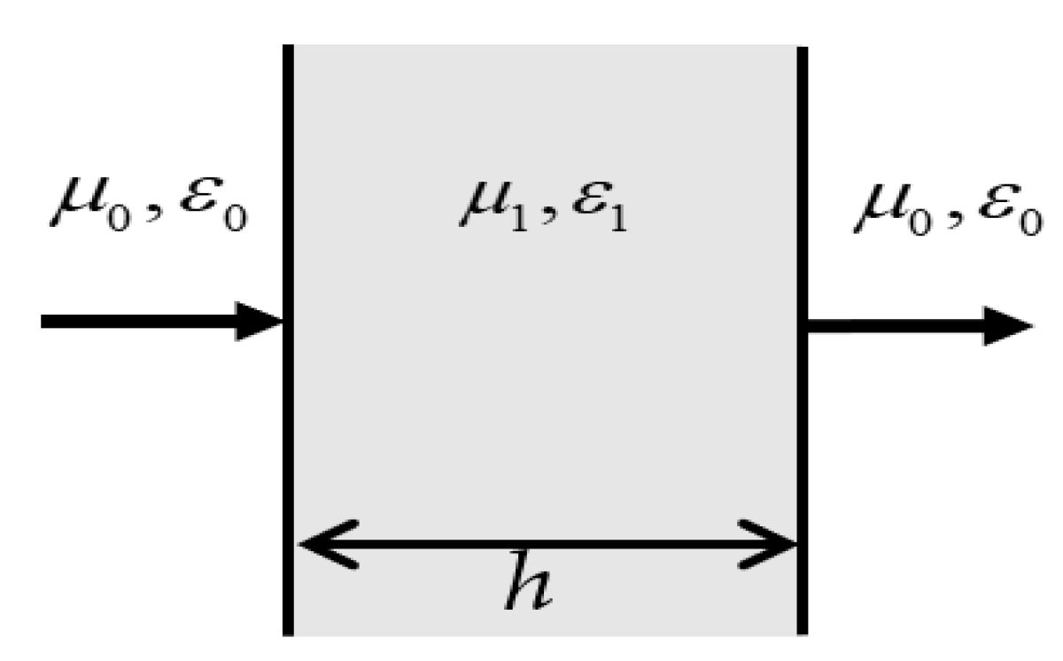
2.1. Wave Propagation Model

Figure 2 shows a millimeter wave incident on a planar dielectric sample with a thickness of h. Transmission occurs at the interface between the sample and air. The total transmitted wave can be calculated using the coefficient [30]
T h = e j β d h ( 1 Γ 2 1 e 2 j β d h Γ 2 )
where
Γ = η d η a η d + η a , β d = 2 π f μ d ε d , η d = μ d ε d , η a = μ a ε a
In the above equations, βd is the wave number inside the dielectric material; ηa and ηd are the intrinsic impedances of free space and dielectric material, respectively; f is the frequency of the millimeter wave incident on the sample.
Equation (1) proves that transmission properties of the sample are related to the material’s permittivity, permeability, and thickness. The material’s dielectric properties are related to process parameters, such as porosity defects. Defects change the dielectric properties of materials [30]. It is consequently important for the system designed in this paper to state that the phase of Ptest changes depending on whether the sample contains cracks.

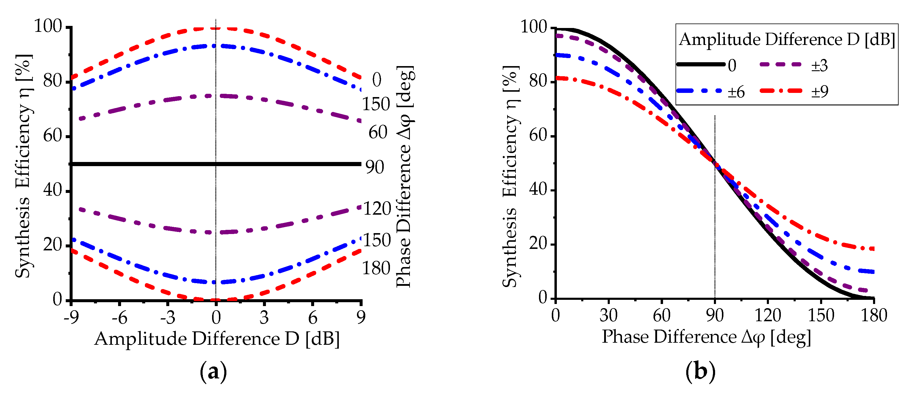
2.2. Theoretical Derivation of Combining Efficiency

As shown in Figure 1, Pc is the output signal of the power combiner, and Ptest and Pref are the two input signals. Suppose that the power amplitudes of Ptest and Pref are ptest and pref, respectively; the phases are φtest and φref, respectively; and the power amplitude of Pc is pc; then, the total output power is [31]
p c = 1 2 | p t e s t e j φ t e s t + p r e f e j φ r e f | 2 = 1 2 [ p t e s t + p r e f + 2 p t e s t p r e f cos ( φ t e s t φ r e f ) ]
Suppose that the amplitude difference and phase difference of Ptest and Pref are D (dB) and ∆φ (deg), respectively, where
D = 10 lg ( p t e s t / p r e f ) and   Δ φ = φ t e s t φ r e f
Then, the combining efficiency can be expressed as
η = p c ( p t e s t + p r e f ) = 1 + 10 D / 10 + 2 × 10 D / 20 × cos Δ φ 2 × ( 1 + 10 D / 10 ) × 100 %
Figure 3 shows the influence of D and ∆φ on the combining efficiency η of the power combiner. Figure 3a shows that when ∆φ is around 90°, η is insensitive to the change in D, but Figure 3b shows that η is very sensitive to the change in ∆φ at this point. This indicates that in the specific range of around 90°, ∆φ is the main factor causing the change of η. Therefore, ∆φ is selected as the test factor, and D remains constant. In order to improve sensitivity of the measurements, the initial conditions of the system should be set as ∆φ = 90° and D = 0 dB. This can be realized by the phase shifter and variable attenuator, respectively.
It is specified that the phases of Ptest, which pass through a standard, non-cracked or tested sample, are φs and φt, respectively. The absolute value of the difference between φs and φt is ∆φt−s, where
Δ φ t s = | φ t φ s |
Suppose that the combining efficiency obtained when testing a standard, non-cracked sample under the initial conditions of D = 0 dB and ∆φ = 90° is ηs. In addition, when φref and D remain constant, the combining efficiency obtained when testing a tested sample is ηt. The absolute value of the difference between ηs and ηt is ∆ηt−s.
Δ η t s = | η t η s | = cos ( 90 Δ φ t s ) 2 = sin ( Δ φ t s ) 2 × 100 %
Through combining the conclusions in Section 2.1., it is clear that ∆φt-s is different due to different sample cracks. Additionally, ∆η varies with ∆φt−s when φref and D remains constant. Therefore, cracks can be determined by different ∆ηt−s values. In the actual experiment, voltages of the signals were measured using detectors and then converted to powers to calculate the combining efficiency. In order to distinguish system errors from the true ∆ηt−s values, ∆ηt−s values greater than 1% were considered as effective values. In other words, cracks that made ∆φt−s greater than 1.2° could be detected by the system.

3. Simulation Validation

The model of subsystem B1 in the proposed system was simulated on Computer Simulation Technology (CST) Microwave Studio (MWS), as shown in Figure 4. This software was used to calculate the functional relationships between ∆φt−s and sample crack properties. Combining the model with Equation (5) allowed the calculation of the relationship between ∆ηt−s and crack properties. The model consisted of two identical horn antennas placed opposite to each other and a tested sample placed at the middle between the antennas. The diameter of both horn antennas was dh, and the spacing between the two antennas was dant. The tested sample was a polytetrafluoroethylene (PTFE) plate with a thickness of 5 mm and a permittivity of 2.55.
In order to characterize the randomness of the target crack, the crack was simplified to the model shown in Figure 5. Parameters describing the crack properties included width w, depth d, length l, and the angle between the crack and the sample axis θ. The initial parameters of the crack were: l = 100 mm, w = 1 mm, d = 1 mm, and θ = 0°.
Figure 6a, Figure 7a and Figure 8a show the relationship between ∆ηt−s and frequency in 30–40 GHz bands with different crack widths, depths, and angles, respectively. It can be seen from these three figures that ∆ηt−s did not vary linearly with frequency but has peaks. The oscillation of these curves was probably caused by the standing wave generated by the changing of the boundary during the signal propagation [32]. As the frequency increased, each curve showed an overall upward trend. This occurred because signals of shorter wavelengths change more in phase as they propagate in dielectric materials [33].
These three figures also show that the system has sensitive frequencies (peak frequencies) when detecting the same crack. We identified through the simulation that the range of sensitive frequencies is not related to the tested sample properties but to the antenna spacing. Therefore, in actual tests, the sensitivity can be improved by adjusting the antenna spacing or the operating frequency. If the operating frequency is fixed, the antenna spacing can be adjusted to ensure the operating frequency is within the sensitive range. Conversely, sensitive frequencies can be used as the operating frequencies when the antenna spacing is given.
The peak frequencies were selected as the operating frequencies, and the values of ∆ηt−s varying with crack properties (w, d, and θ) were calculated using Equation (5). As shown in Figure 6b and Figure 7b, ∆ηt−s increased with the increase in w and d, respectively, at the peak frequencies. However, the value of ∆ηt−s at a higher frequency was greater. This indicates that the system was more sensitive at a higher peak frequency.
Figure 8b shows that ∆ηt−s decreased with the increase in θ. This shows that the sensitivity of the system is related to the angle between the polarization direction of the millimeter wave and the crack direction. In addition, the sensitivity was highest when the crack direction was orthogonal to the electric field direction of the millimeter wave. Meanwhile, the testing sensitivity was axisymmetric, with an axis of symmetry of 90°. Therefore, in actual tests, the sample can be rotated and tested at different angles, which can prevent the crack from missing detection.
Figure 6 shows that for the PTFE sample used in the system, a 0.4 mm wide crack (crack depth was 1 mm and length was 100 mm) could be detected at the lower peak frequency of 35 GHz, which was about 0.07 times the wavelength of the signal propagating in the sample (λg). In addition, a crack with a width of 0.2 mm, which is about 0.04λg, could be detected at the higher peak frequency of 39 GHz. Figure 7 illustrates that the system could detect a crack with a depth of 0.4 mm at 35 GHz and a crack with a depth of 0.2 mm at 39 GHz. Overall, the system can detect cracks with a minimum width of 0.2 mm and a minimum depth of 0.2 mm in the Ka band, which can cause the signal phase to change by more than 1.2°.

4. Experimental Validation

Once the feasibility of using combining efficiency to detect whether dielectric materials contain cracks was verified through the simulation, an experimental validation on a set of PTFE plates with cracks of different widths was performed. The goal was to demonstrate the validity of the system for crack detection, which can be accomplished using a lower sensitive frequency and larger cracks [28].

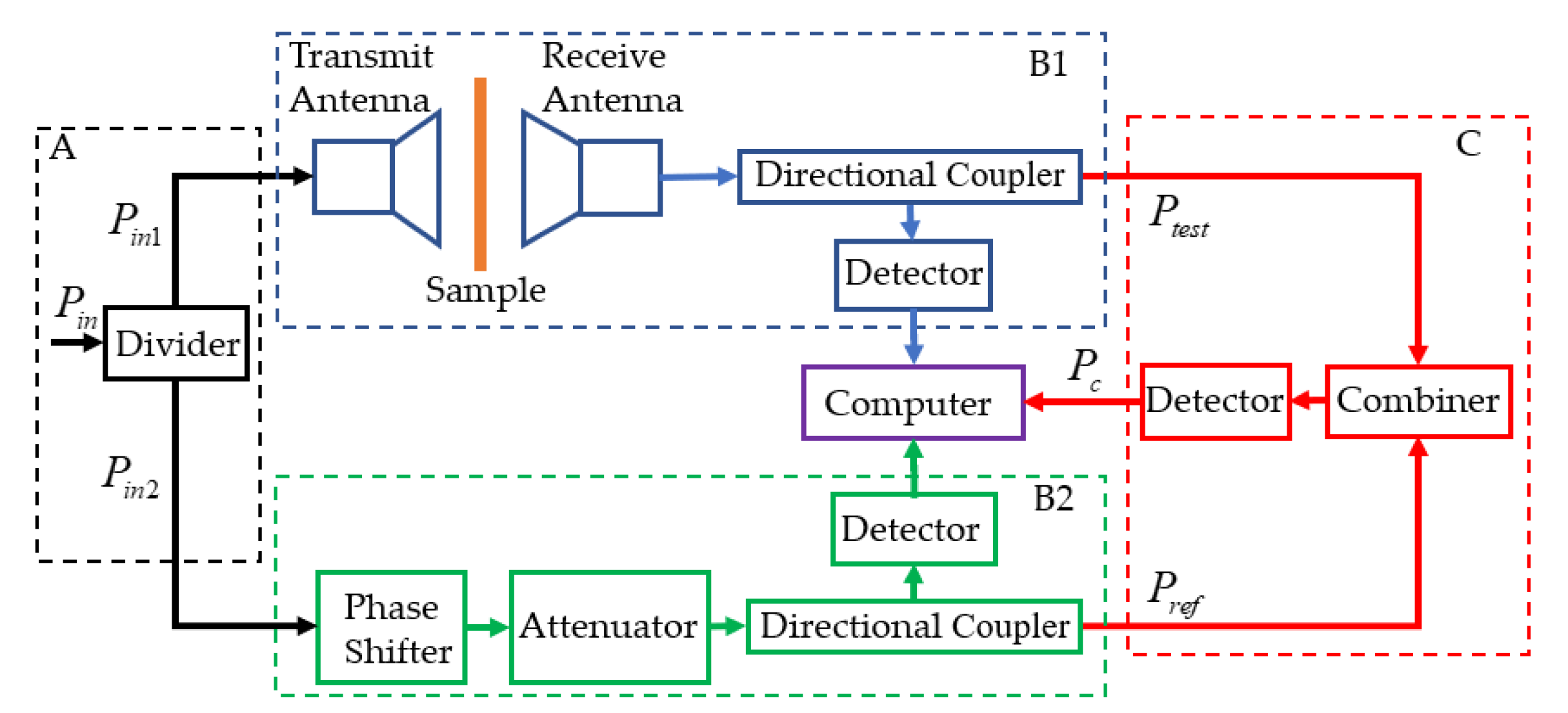
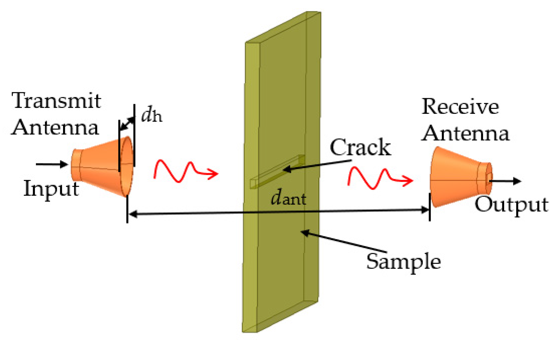
4.1. Measurement System

As shown in Figure 9, an experimental system was built according to Figure 1. A transceiver system with an operating frequency of 35 GHz was used for the generation of the excitation signal, which was a square wave signal with a duty cycle of 20%. The power divider and the power combiner were two identical E-T waveguide junctions. Two antennas with a model number of HD320LHA50 from Hengda Microwave Co., Ltd, Xian, China. were used as the transmit antenna and receive antenna. The diameter of both antennas was 50 mm, and the antenna spacing was 300 mm, which allowed an operating frequency of 35 GHz to be the sensitive frequency of the system. The signal voltages were measured by three identical detectors. Detector 1 and detector 3 measured the voltage of the signal coupled from the directional coupler in subsystems B1 and B2, respectively, and detector 2 detected the voltage of the combined signal. The detected results were V1, V2, and Vc, respectively. In order to reduce the error caused by reflection due to the mismatch between the device ports, four 40 dB isolators were added to the system.
According to the conclusions in Section 2.2., it was necessary to initialize the system to improve measurement sensitivity. The specific setting steps were: (1) Put the non-cracked PTFE sample into the system. Adjust the values of V1 and V2 to be equal by the variable attenuator to ensure that D = 0 dB. (2) Use the phase shifter to adjust the phase of Pref so that Vc = 0, which indicates that ∆φ = 0° or 180°. (3) Use the phase shifter to change the phase of Pref by about 90°.

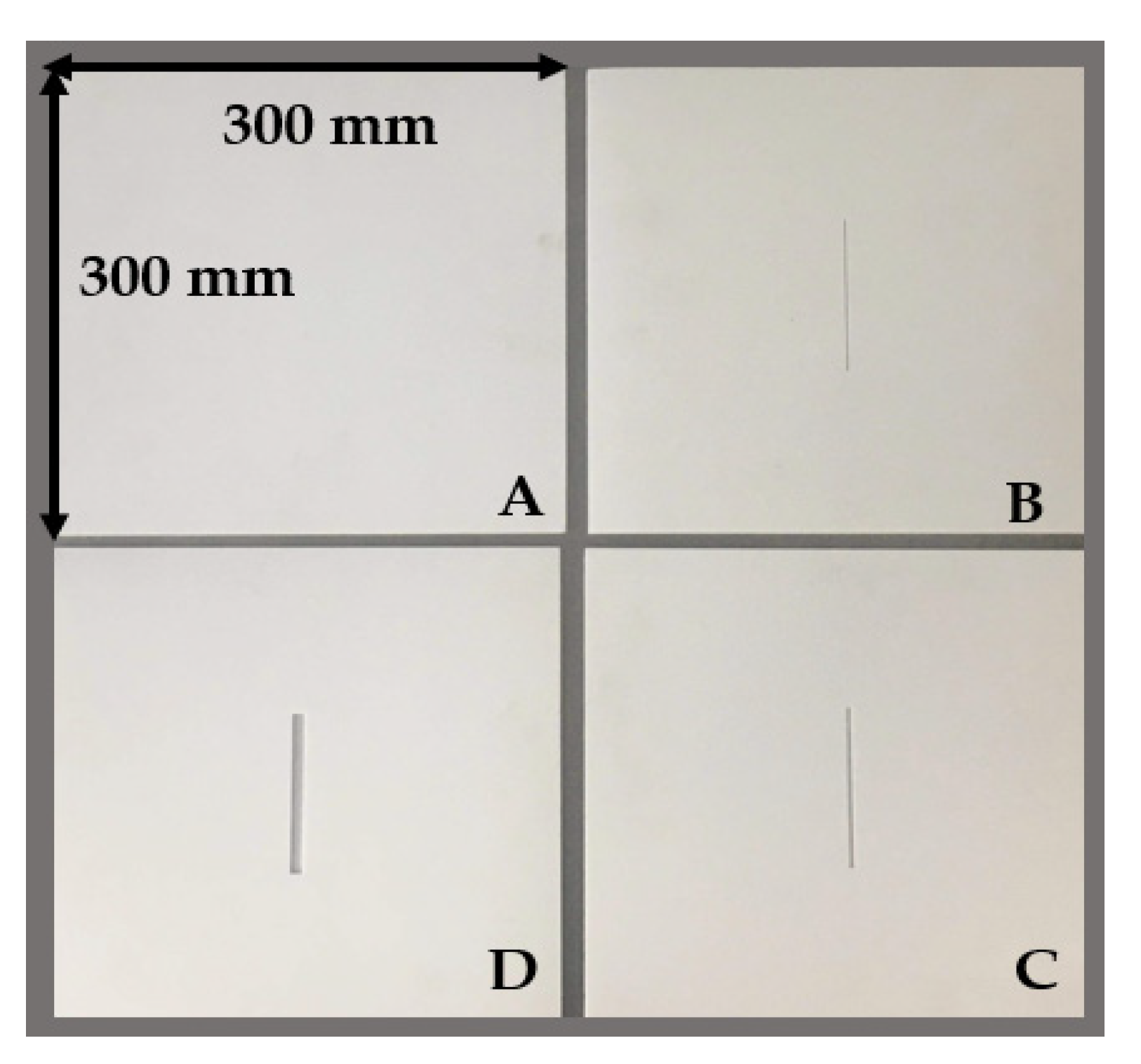
4.2. Samples under Test

In total, 4 PTFE sample plates with a size of 300 × 300 × 5 mm3 were made. One was a standard sample (sample A) without any cracks, and the remaining three (samples B, C, and D) contained cracks of different widths. The length of the cracks was 100 mm, and the depth was 1 mm. In addition, the width of the cracks was 1, 3, and 7 mm, respectively. Since the field radiating from the antenna to the sample is strongest along the central axis of the antenna, a crack located at the center of the sample can cause the greatest change in the field. In other words, the system has the highest sensitivity to detect the crack when it is located at the center of the sample. From the conclusions in Section 3, it is clear that the test sensitivity is highest when the angle of the crack is 0°. To simplify the experimental verification, the crack in the sample was located in the center of the sample and parallel to the edge of the sample. In other words, the crack angle as described in Figure 5 was 0°. In actual tests, the crack angle can be changed by rotating the sample. A photograph of the samples used for the test is shown in Figure 10.

4.3. Measurement Result

The samples in Figure 10 were placed in order at the middle of the antennas. Then, the voltages V1, V2, and Vc were obtained with a single measurement. The combining efficiency ηs of measuring sample A was calculated for V1, V2, and Vc. Then, it was replaced with a remaining tested sample while the phase shifter was kept unchanged. Meanwhile, the variable attenuator was adjusted to keep V1 = V2, which kept φref and D constant. Subsequently, the combining efficiency ηt was measured. Finally, cracks were determined by the difference between ηt and ηs (∆ηt−s).
The four samples were tested repeatedly N times, and the corresponding combining efficiencies were calculated. A statistical analysis was carried out on the test results. The average value ( η ¯ ), standard deviation (SD), and relative error (Error) of the combining efficiencies corresponding to each sample were calculated as shown in Table 1. It can be seen that the system error was less than 1% when testing the same sample, and the standard deviation was less than 0.3, which indicates that the system exhibits good stability and reproducibility.
The experimental results in Table 1 show that each 1 mm difference in the width of the crack in the PTFE samples corresponds to a value of ~4% of ∆ηt−s. This illustrates that the experimental system can detect cracks with a width of ~0.4 mm (a length of 100 mm and a depth of 1 mm) at 35 GHz. The simulation results, experimental results, and the theoretical derivation are in good agreement, which proves the feasibility of the method to detect cracks that can make the signal phase change by more than 1.2°.

5. Conclusions

A method of millimeter-wave NDT for dielectric material cracks based on millimeter-wave interference is proposed in this paper. From the results of theoretical analysis, simulations, and experiments, the following conclusions were obtained:
(1)
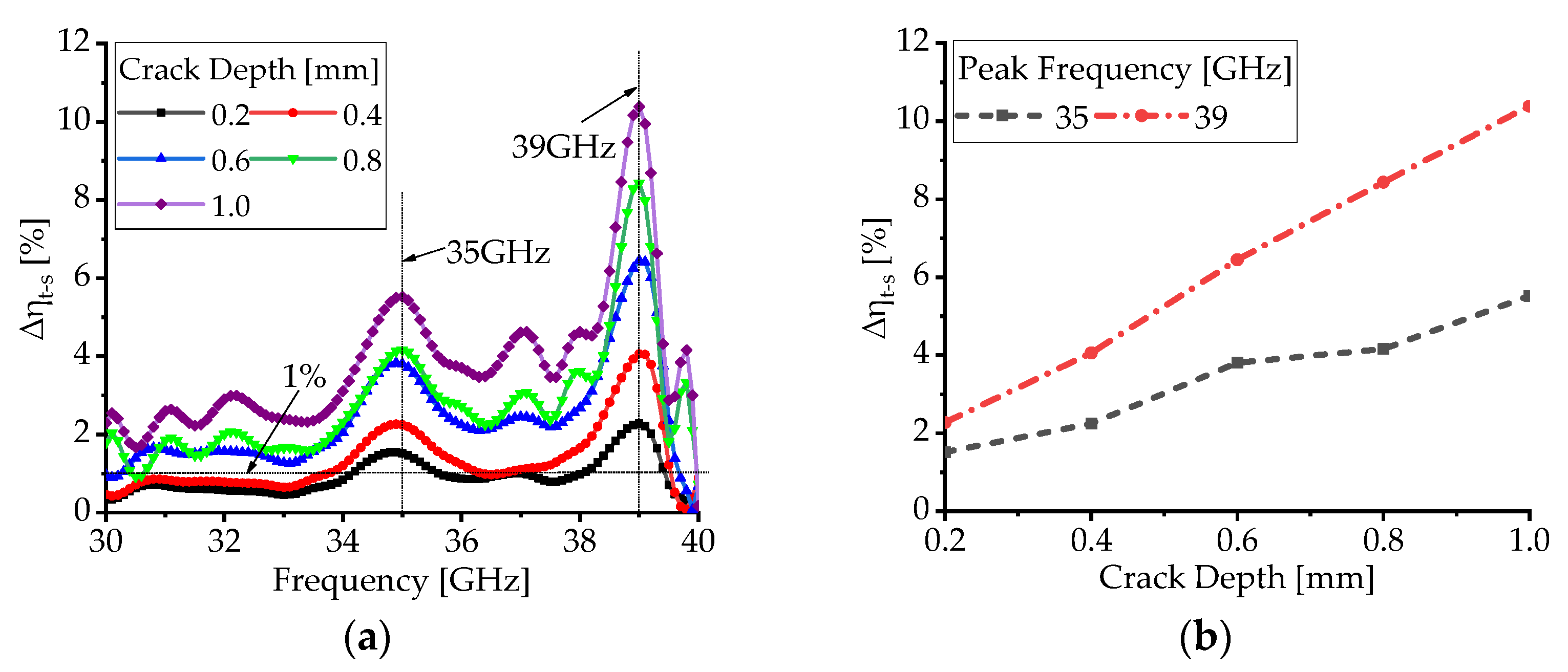
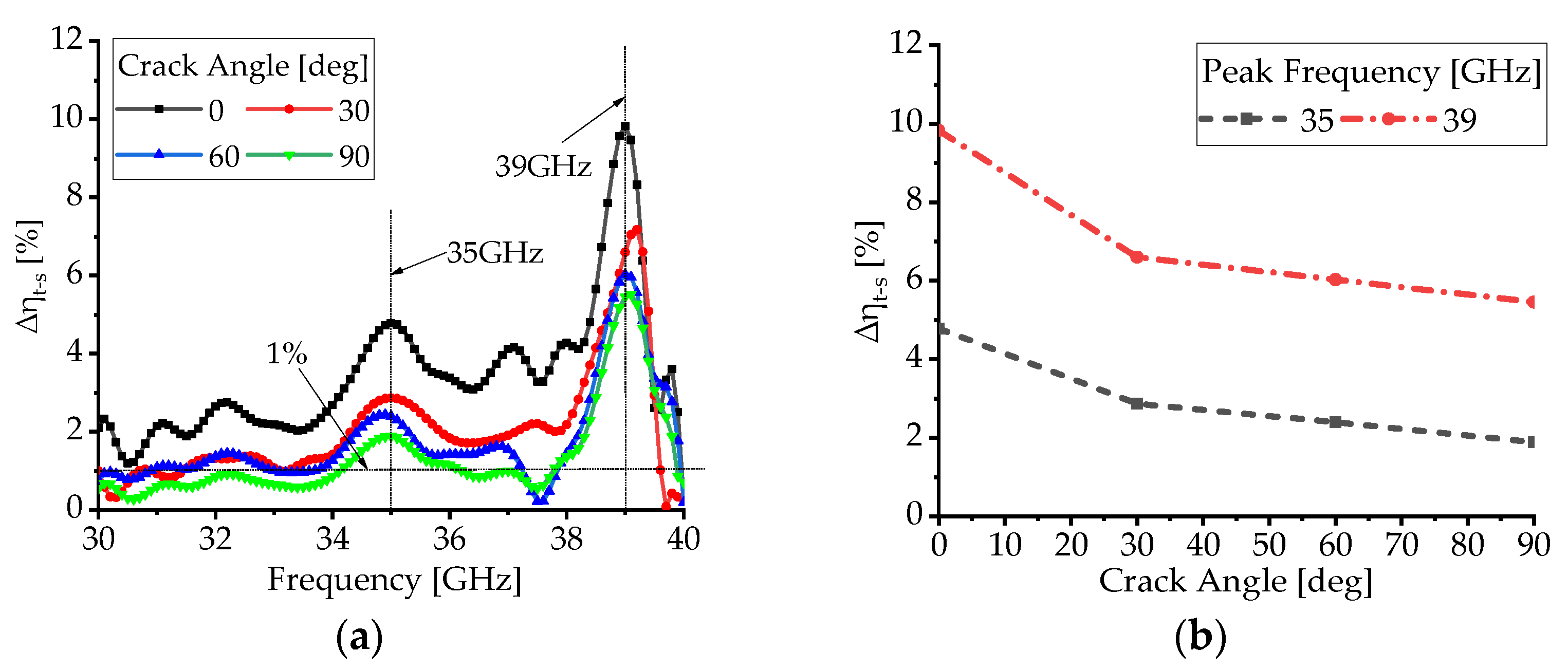
Under specific conditions, this method can detect cracks that make the signal phase change more than 1.2°, corresponding to a combining efficiency difference of more than 1%.
(2)
The sensitivity of the system can be improved by changing the operating frequency or the antenna spacing.
(3)
The experimental system developed using this method has a system error of less than 1% when testing the same sample. In addition, the system exhibits good stability and reproducibility.
(4)
For PTFE materials with a thickness of 5 mm and a permittivity of 2.55, each 1 mm difference in the crack width corresponds to a combining efficiency difference of ~4%. Cracks with a width of ~0.4 mm, which is ~0.07 λg, can be detected at 35 GHz.
The NDT method proposed in this paper is not limited to detecting cracks: it can also be used to measure material thickness, permittivity, and so on. Furthermore, this method has the potential for large-scale online applications in various industries due to its simplistic, fast, low-cost, and efficient characteristics. The results of this paper are just a preliminary verification of the feasibility of crack detection using this method. In the future, we will consider optimizing the system to improve the testing sensitivity to detect microcracks and improve the detection function to obtain specific information about the cracks, such as size, shape, and location.

Author Contributions

Conceptualization, L.C. and Y.Y.; methodology, L.C. and Y.Y.; validation, L.C., B.W. and H.L.; formal analysis, L.B.; investigation, Y.Q.; writing—original draft preparation, L.C.; writing—review and editing, L.B., M.S., and Y.Q.; project administration, L.M.; funding acquisition, Y.Y. All authors have read and agreed to the published version of the manuscript.

Funding

This work was supported in part by the National Natural Science Foundation of China under grants 61671116, 61771096, and 11905026; in part by the National Key Research and Development Program of China under grant 2019YFA0210202; and in part by the Fundamental Research Funds for the Central Universities under grants ZYGX2019Z006 and ZYGX2019J012.

Data Availability Statement

Data is contained within the article.

Conflicts of Interest

The authors declare no conflict of interest.

References

  1. Amineh, R.K.; Ravan, M.; Sharma, R. Nondestructive Testing of Nonmetallic Pipes Using Wideband Microwave Measurements. IEEE Trans. Microwave Theory Tech. 2020, 68, 1763–1772. [Google Scholar] [CrossRef]
  2. Song, G.R.; Yan, T.T.; He, C.F.; Yang, S.; Lu, Y.; Wu, B. Detection of surface crack on the substrate under thermal barrier coatings using microwave non-destructive evaluation. J. Microwave Power. 2015, 49, 69–75. [Google Scholar]
  3. Ciampa, F.; Mahmoodi, P.; Pinto, F.; Meo, M. Recent advances in active infrared thermography for non-destructive testing of aerospace components. Sensors 2018, 18, 609. [Google Scholar] [CrossRef] [Green Version]
  4. Wang, Z.; Tian, G.Y.; Meo, M.; Ciampa, F. Image processing based quantitative damage evaluation in composites with long pulse thermography. NDT&E Int. 2018, 99, 93–104. [Google Scholar]
  5. Bastianini, F.; Tommaso, D.A.; Pascale, G. Ultrasonic non-destructive assessment of bonding defects in composite structural strengthenings. Compos. Struct. 2001, 53, 3–7. [Google Scholar]
  6. Garcea, S.C.; Wang, Y.; Withers, P.J. X-ray computed tomography of polymer composites. Compos. Sci. Technol. 2018, 156, 5–19. [Google Scholar] [CrossRef]
  7. Schilling, P.J.; Karedla, B.R.; Tatiparthi, A.K.; Verges, M.A.; Herrington, P.D. X-ray computed microtomography of internal damage in fiber reinforced polymer matrix composites. Compos. Sci. Technol. 2005, 65, 1–8. [Google Scholar] [CrossRef]
  8. Tsukada, K.; Hayashi, M.; Nakamura, Y.; Sakai, K.; Kiwa, T. Small Eddy Current Testing Sensor Probe Using a Tunneling Magnetoresistance Sensor to Detect Cracks in Steel Structures. IEEE Trans. Magn. 2018, 54, 1–5. [Google Scholar] [CrossRef]
  9. Duchene, P.; Chaki, S.; Ayadi, A.; Krawczak, P. A review of non-destructive techniques used for mechanical damage assessment in polymer composites. J. Mater. Sci. 2018, 53, 7915–7938. [Google Scholar] [CrossRef]
  10. Zhang, H.; Yang, R.; He, Y.; Foudazi, A.; Cheng, L.; Tian, G. A Review of Microwave Thermography Nondestructive Testing and Evaluation. Sensors 2017, 17, 1123. [Google Scholar] [CrossRef]
  11. Liu, L. Application of Microwave for Remote NDT and Distinction of Biofouling and Wall Thinning Defects Inside a Metal Pipe. J. Nondestruct. Eval. 2015, 34, 40. [Google Scholar] [CrossRef]
  12. Sutthaweekul, R.; Tian, G.Y.; Wang, Z.J.; Ciampa, F. Microwave open-ended waveguide for detection and characterisation of FBHs in coated GFRP pipes. Compos. Struct. 2019, 225, 111080. [Google Scholar] [CrossRef]
  13. Shrifan, N.H.M.M.; Akbar, M.F.; Isa, N.A.M. Prospect of Using Artificial Intelligence for Microwave Nondestructive Testing Technique: A Review. IEEE Access 2019, 7, 110628–110650. [Google Scholar] [CrossRef]
  14. Shrifan, N.H.M.M.; Jawad, G.N.; Isa, N.A.M.; Akbar, M.F. Microwave Nondestructive Testing for Defect Detection in Composites Based on K-Means Clustering Algorithm. IEEE Access 2021, 9, 4820–4828. [Google Scholar] [CrossRef]
  15. Chizh, M.; Zhuravlev, A.; Razevig, V.; Ivashov, S.; Falorni, P.; Capineri, L. Defects investigation in thermal insulation coatings with microwave imaging based on a 22 GHz holographic radar. NDT&E Int. 2020, 109, 102191. [Google Scholar]
  16. Arbaoui, A.; Ouahabi, A.; Jacques, S.; Hamiane, M. Concrete Cracks "Detection and Monitoring Using Deep Learning-Based Multiresolution Analysis. Electronics 2021, 10, 1772. [Google Scholar] [CrossRef]
  17. Rahman, M.S.; Haryono, A.; Abou-Khousa, M.A. Microwave Non-destructive Evaluation of Glass Reinforced Epoxy and High-Density Polyethylene Pipes. J. Nondestruct. Eval. 2020, 39, 26. [Google Scholar] [CrossRef]
  18. Shirai, H.; Sekiguchi, H. A simple crack depth estimation method from backscattering response. IEEE Trans. Instrum. Meas. 2004, 53, 1249–1254. [Google Scholar] [CrossRef]
  19. Roqueta, G.; Jofre, L.; Feng, M.Q. Analysis of the Electromagnetic Signature of Reinforced Concrete Structures for Nondestructive Evaluation of Corrosion Damage. IEEE Trans. Instrum. Meas. 2012, 61, 1090–1098. [Google Scholar] [CrossRef] [Green Version]
  20. Kharkovsky, S.; McClanahan, A.; Zoughi, R.; Palmer, D.D. Microwave Dielectric-Loaded Rectangular Waveguide Resonator for Depth Evaluation of Shallow Flaws in Metals. IEEE Trans. Instrum. Meas. 2011, 60, 3923–3930. [Google Scholar] [CrossRef]
  21. Zoughi, R.; Gallion, J.R.; Ghasr, M.T. Accurate Microwave Measurement of Coating Thickness on Carbon Composite Substrates. IEEE Trans. Instrum. Meas. 2016, 65, 951–953. [Google Scholar] [CrossRef]
  22. Gal, B.; Nowak, D. Nondestructive, Microwave Testing of Compression Strength and Moisture Content of Green Molding Sands. J. Nondestruct. Eval. 2021, 40, 86. [Google Scholar] [CrossRef]
  23. Gao, Y.; Ravan, M.; Amineh, K.R. Fast, Robust, and Low-Cost Microwave Imaging of Multiple Non-Metallic Pipes. Electronics 2021, 10, 1762. [Google Scholar] [CrossRef]
  24. Wu, H.; Amineh, R.K. A Low-Cost and Compact Three-Dimensional Microwave Holographic Imaging System. Electronics 2019, 8, 1036. [Google Scholar] [CrossRef] [Green Version]
  25. Chen, G.; Katagiri, T.; Song, H.; Yusa, N.; Hashizume, H. Detection of cracks with arbitrary orientations in a metal pipe using linearly-polarized circular TE11 mode microwaves. NDT&E Int. 2019, 107, 102125. [Google Scholar]
  26. Li, W.; Li, Y.; Tan, J.; Abidin IM, Z.; Hu, J.; Chen, Z.; Wu, Y. A Millimetre-wave Probe for Fast Screening and Evaluation of Corrosion in Planar Conductors: Numerical Simulations. IOP Conf. Ser. Mater. Sci. Eng. 2019, 554, 012003. [Google Scholar] [CrossRef]
  27. Nazarchuk, Z.T.; Dzhala, V.R.; Synyavs’kyi, A.T. Detection of Subsurface Inhomogeneities in Dielectric Materials by the Microwave method. Mater. Sci. 2014, 49, 425–441. [Google Scholar] [CrossRef]
  28. McClanahan, A.; Kharkovsky, S.; Maxon, A.R.; Zoughi, R.; Palmer, D.D., Jr. Depth Evaluation of Shallow Surface Cracks in Metals Using Rectangular Waveguides at Millimeter-Wave Frequencies Depth Evaluation of Shallow Surface Cracks. IEEE Trans. Instrum. Meas. 2010, 59, 1693–1704. [Google Scholar] [CrossRef]
  29. Mukherjee, S.; Tamburrino, A.; Haq, M.; Udpa, S.; Udpa, L. Far field microwave NDE of composite structures using time reversal mirror. NDT&E Int. 2018, 93, 7–17. [Google Scholar]
  30. Arunachalam, K.; Melapudi, V.R.; Udpa, L.; Udpa, S.S. Microwave NDT of cement-based materials using far-field reflection coefficients. NDT&E Int. 2006, 39, 585–593. [Google Scholar]
  31. Gupta, M.S. Power Combined Efficiency and its Optimization. IEE Proc. Part H Microwaves Opt. Antennas. 1992, 139, 233–238. [Google Scholar] [CrossRef]
  32. Yassin, A.; Rahman, M.S.U.; Abou-Khousa, M.A. Imaging of Near-Surface Defects using Microwaves and Ultrasonic Phased Array Techniques. J. Nondestruct. Eval. 2018, 37, 71. [Google Scholar] [CrossRef]
  33. Chen, G.; Katagiri, T.; Song, H.; Yusa, N.; Hashizume, H. Investigation of the effect of a bend on pipe inspection using microwave NDT. NDT&E Int. 2020, 110, 102208. [Google Scholar]
Figure 1. Block diagram of the system designed based on the proposed method.
Electronics 11 00583 g001
Figure 2. Transmission of millimeter wave at normal incidence on dielectric slab with a thickness of h. μa and μd are the permeability of free space and dielectric material, respectively; εa and εd are the permittivity of free space and dielectric material, respectively.
Electronics 11 00583 g002
Figure 3. The influence of D and ∆φ on the power combining efficiency η. (a) The influence of D on η when ∆φ remains constant. (b) The influence of ∆φ on η when D remains constant.
Electronics 11 00583 g003
Figure 4. Detection system model built on CST MWS (not to scale).
Electronics 11 00583 g004
Figure 5. Schematic diagram of the crack in the tested sample: (a) plan view and (b) side view (not to scale).
Electronics 11 00583 g005
Figure 6. Simulation results of cracks of different widths in 30–40 GHz bands. (a) Corresponding to different values of w, the relationship between ∆ηt−s and frequency when d = 1 mm, l = 100 mm, and θ = 0°. (b) The relationship between ∆ηt−s and w at different peak frequencies when d = 1 mm, l = 100 mm, and θ = 0°.
Electronics 11 00583 g006
Figure 7. Simulation results of cracks of different depths in 30–40 GHz bands. (a) Corresponding to different values of d, the relationship between ∆ηt−s and frequency when w = 1 mm, l = 100 mm, and θ = 0°. (b) The relationship between ∆ηt−s and d at different peak frequencies when w = 1 mm, l = 100 mm, and θ = 0°.
Electronics 11 00583 g007
Figure 8. Simulation results for cracks of different angles in 30–40 GHz bands. (a) Corresponding to different values of θ, the relationship between ∆ηt−s and frequency when w = 1, d = 1, and l = 100 mm. (b) The relationship between ∆ηt−s and θ at different peak frequencies when w = 1, d = 1, and l = 100 mm.
Electronics 11 00583 g008
Figure 9. Photograph of the test system.
Electronics 11 00583 g009
Figure 10. Photograph of the PTFE samples used for the test. Sample (A) is the non-cracked sample. The crack width of sample (B) is 1 mm. The crack width of sample (C) is 3 mm. Finally, the crack width of sample (D) is 7 mm.
Electronics 11 00583 g010
Table 1. Statistical analysis results of the measurement data of 5 samples.
SampleStandardABC
N50505050
η ¯ (%)55.40660.38266.76381.727
SD0.2350.2060.1540.280
Error (%)0.8570.6240.5800.797
ηt−s (%)-4.97611.35726.321
Publisher’s Note: MDPI stays neutral with regard to jurisdictional claims in published maps and institutional affiliations.

