Article

A Calibration-Free, 16-Channel, 50-MS/s, 14-Bit, Pipelined-SAR ADC with Reference/Op-Amp Sharing and Optimized Stage Resolution Distribution

State Key Laboratory of ASIC & System, Fudan University, Shanghai 201203, China
*
Authors to whom correspondence should be addressed.
Electronics 2022, 11(5), 749; https://doi.org/10.3390/electronics11050749
Submission received: 30 January 2022 / Revised: 21 February 2022 / Accepted: 25 February 2022 / Published: 28 February 2022
(This article belongs to the Section Microelectronics)

Abstract

:
This paper presents a calibration-free, 16-channel, 14-bit, 50-MS/s, pipelined successive approximation register (pipelined-SAR) analog-to-digital converter (ADC) for ultrasound imaging systems. A reference sharing scheme with reduced buffers is proposed to improve area-and-power efficiency, which is essential for multi-channel systems. Based on this, a three-stage, pipelined-SAR ADC architecture with reference/op-amp sharing and optimized stage resolution distribution is proposed. The prototype ADC is designed in a 0.18-μm process with peripheral circuits integrated, including low-voltage differential signaling (LVDS), bandgap, etc. It achieves a robust and calibration-free performance with 68.25-dB signal to noise and distortion ratio (SNDR) and 82.19-dB spurious-free dynamic range (SFDR), translating into a competitive figure of merit (FoM) of 0.47 pJ/conversion-step among other high-resolution ADCs used in ultrasound applications.

1. Introduction

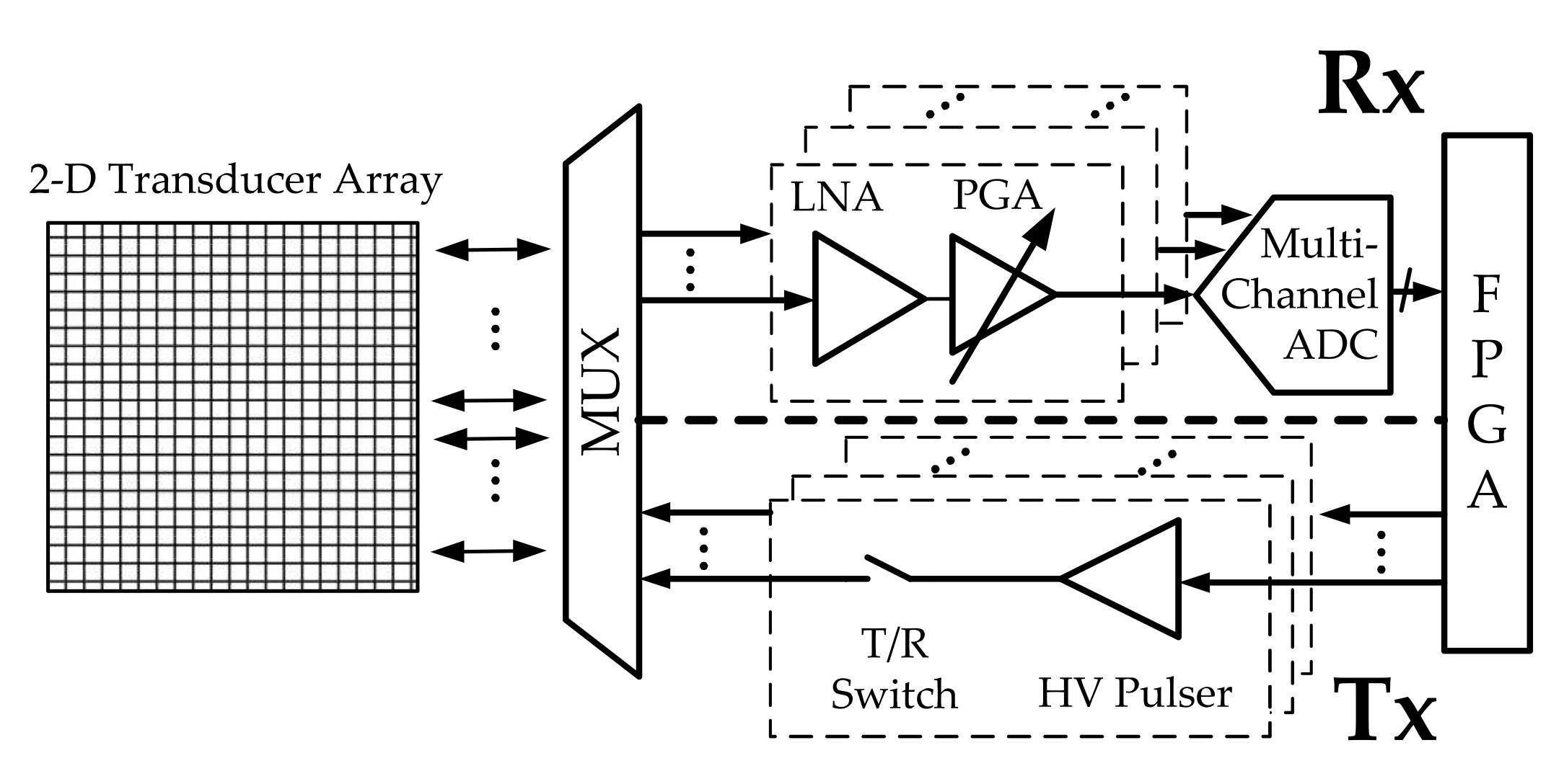
1.1. Ultrasound Imaging System

Ultrasound imaging is widely used in non-destructive testing and medical examination because it is simple, cheap, and non-invasive [1,2,3]. With the development of phased array and synthetic aperture technology, the number of receiving (RX) and transmitting (TX) channels in ultrasound imaging systems is increasing to obtain a larger scan range and higher resolution [4,5]. Figure 1 illustrates a typical ultrasound imaging system.
During the TX phase, the high-voltage (HV) pulsers emit pulses that go through the transmit-and-receive (T/R) switches and the multiplexer (MUX), exciting transducers, generating ultrasonic waves. After being reflected by the target to be measured, the echo signal is converted into an electrical signal by the transducer. The electrical signal is first amplified by the low noise amplifiers (LNA), then by the programmable gain amplifiers (PGA) according to the attenuation during propagation. After being quantized by a multi-channel ADC, it is sent to a field programmable gate array (FPGA) for imaging.
The ADC often becomes the bottleneck of the whole system [6]. It not only determines the final signal-to-noise ratio (SNR) of the images but also significantly affects the complexity of the entire circuit system. The more channels integrated into a single chip, the more compact the system can be.
Therefore, the trend of ADCs for high-end ultrasound imaging systems is to increase the number of channels while maintaining high resolution [7,8,9]. The resolution of the ADCs is 12-bit or more. Thanks to the limited bandwidth of ultrasound signal, which is usually less than 10 MHz, the requirement for ADC sampling rate is eased. The pipelined-SAR architecture that achieves high area-and-power efficiency becomes an attractive option in such multi-channel, high-precision, medium-speed scenarios.

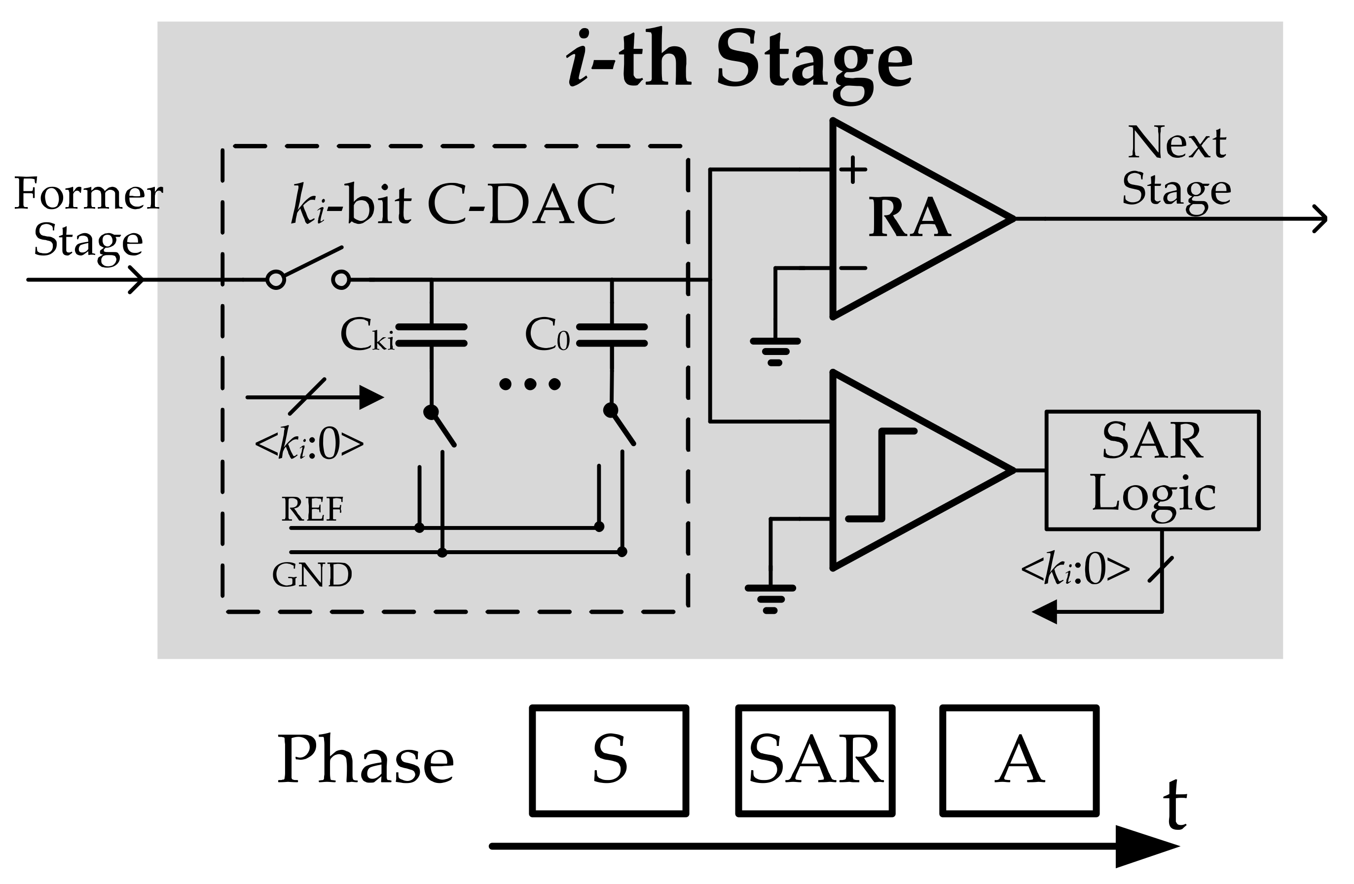
1.2. Pipelined-SAR ADC

Figure 2 illustrates the architecture of a pipelined-SAR ADC. Compared with the traditional pipeline architecture, SAR rather than flash ADC is adopted as the sub-ADC of each pipeline stage, achieving a good balance between conversion speed and power consumption. Each pipeline stage consists of a residue amplifier (RA) that is usually a high precision operational amplifier (op-amp) and a ki-bit SAR ADC that includes a capacitive DAC (C-DAC), comparator, and SAR logic. Correspondingly, the operating cycle of a pipeline stage is divided into three phases: Sampling (S), SAR conversion (SAR), and Amplification (A).
Several efforts have been made to improve the area-and-power efficiency of pipelined-SAR ADCs, which is critical in a multi-channel application. A popular and effective improvement is to replace the power-hungry op-amps with amplifiers without DC power consumption, such as ringamp [10,11], dynamic amplifiers [12,13], or to use open-loop amplifiers [14,15]. Though these designs significantly reduce the power consumption of RA, they suffer from PVT fluctuations and often rely on complex background calibration. Since the performance uniformity between channels is also essential in ultrasound imaging systems, traditional op-amps with a robust closed-loop structure are preferred. Another method is to use the half-gain technique, which halves the gain of the RA, reducing the signal swing and easing the requirement of RA [16,17]. However, this method requires that the reference voltages of the post-stages are also halved, increasing the complexity of the reference circuit. Op-amp sharing technique, which is popular in pipeline ADCs and can also save in power consumption of the op-amps, is seldom used in pipelined-SAR architecture because it takes extra time to eliminate memory effect, degrading the sampling rate. While for medium-speed applications, it remains effective and will be further introduced in the following sections.
In addition, many of the optimization techniques applied to SAR ADCs can also be applied to multi-stage pipeline-SAR ADCs, such as efficient switching schemes [18,19,20], redundant trails in SAR conversion, which alleviate the requirements for comparator offset and MSB settlement [21]. Finally, as digital circuits benefit more from process development, more designs tend to use digital calibration methods to compensate for analog circuits, such as split-channel-based architectures that can calibrate both capacitor arrays and amplifiers [22].
However, little attention is paid to another power-hungry but essential circuit block, reference, which is explained in detail in the following section. Besides, ADCs in ultrasound applications usually need to be integrated with analog frontends (AFE) and sometimes HV circuits to realize higher system integration. It leads to the necessity to use mature processes with high supply voltage to guarantee a large dynamic range, making a significant overhead of digital calibration. Thus, aggressive circuit simplification based on digital calibration is not favored.

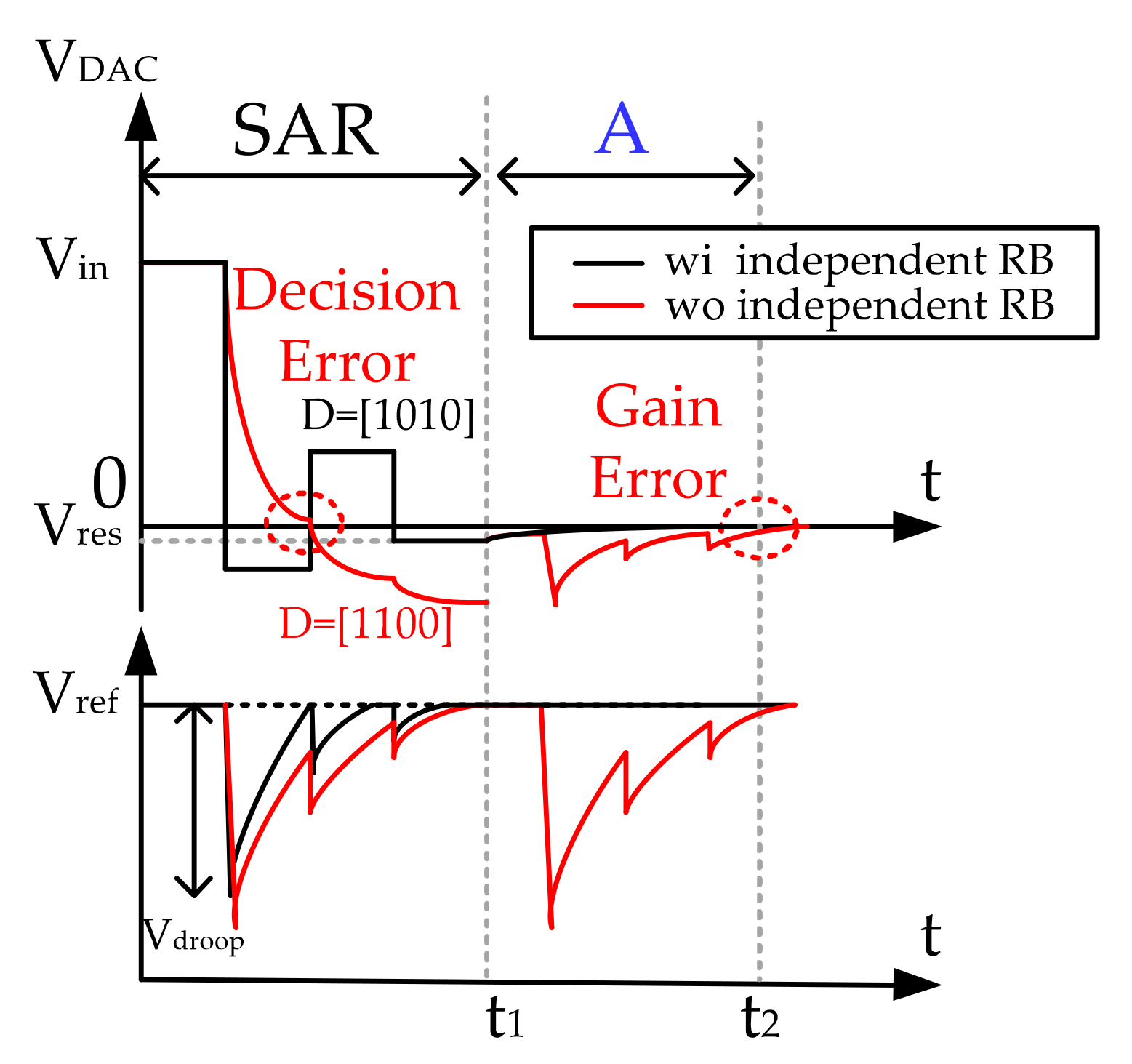
1.3. Reference Considerations in Pipelined-SAR ADCs

In a pipelined-SAR ADC, each pipeline stage needs a pair (positive and negative) of stable references to finish the SAR conversion and to hold the residual voltage left on the top plate of the C-DAC during amplification. Figure 3 illustrates the transient waveforms of residual voltages and the output (Vref) of a positive reference buffer (RB) during SAR and Amplification phase. A decreasing droop is generated on the reference during the SAR phases. Suppose the ripple does not disappear before the next trial starts; a decision error may occur, which cannot be corrected if there is no sufficient redundancy in the capacitor array. When in the Amplification phase, the ripple on the reference will cause fluctuation on the residual voltage, and a noise-like gain error may be introduced and degrades the SNR.
To reduce the ripple in the SAR phase, it is necessary to use either larger decoupling capacitors [23,24] which occupy more area, or reduce the output resistance of reference buffers [25,26], making them more power-hungry. To avoid the gain error, the reference connected to the C-DAC should be idle during the Amplification phase. Thus, allocating an independent reference buffer for each stage becomes an optimal solution [27], where significant area and power can be saved if the number of buffers needed is reduced.
According to the discussion above, a reference sharing scheme is proposed with one-third of reference buffers reduced and no performance tradeoff. The scheme is a generic method applicable to all pipelined-SAR ADCs with three or more stages, effectively improving the area-and-power efficiency.
Based on the reference sharing scheme, a calibration-free, 16-channel, 50-MS/s, 14-bit ADC for ultrasound imaging systems is designed and measured. The area-and-power efficiency of the ADC is further improved by the op-amp sharing technique and optimization of the stage resolution distribution. The proposed ADC is fabricated in a 0.18-μm process. The measurement results show that it achieves a robust and competitive performance without calibration, and can be easily further integrated with AFEs.
This paper is organized as follows. Section 2 explains the proposed reference sharing scheme used in multi-stage pipelined-SAR ADCs. Section 3 analyzes the impact on the area and power consumption caused by stage resolution distribution, proposing an optimized architecture for a 14-bit resolution ADC. Section 4 and Section 5 show the structure and circuit implementation of the proposed ADC. Measurement results are shown in Section 6. Section 7 concludes this paper.

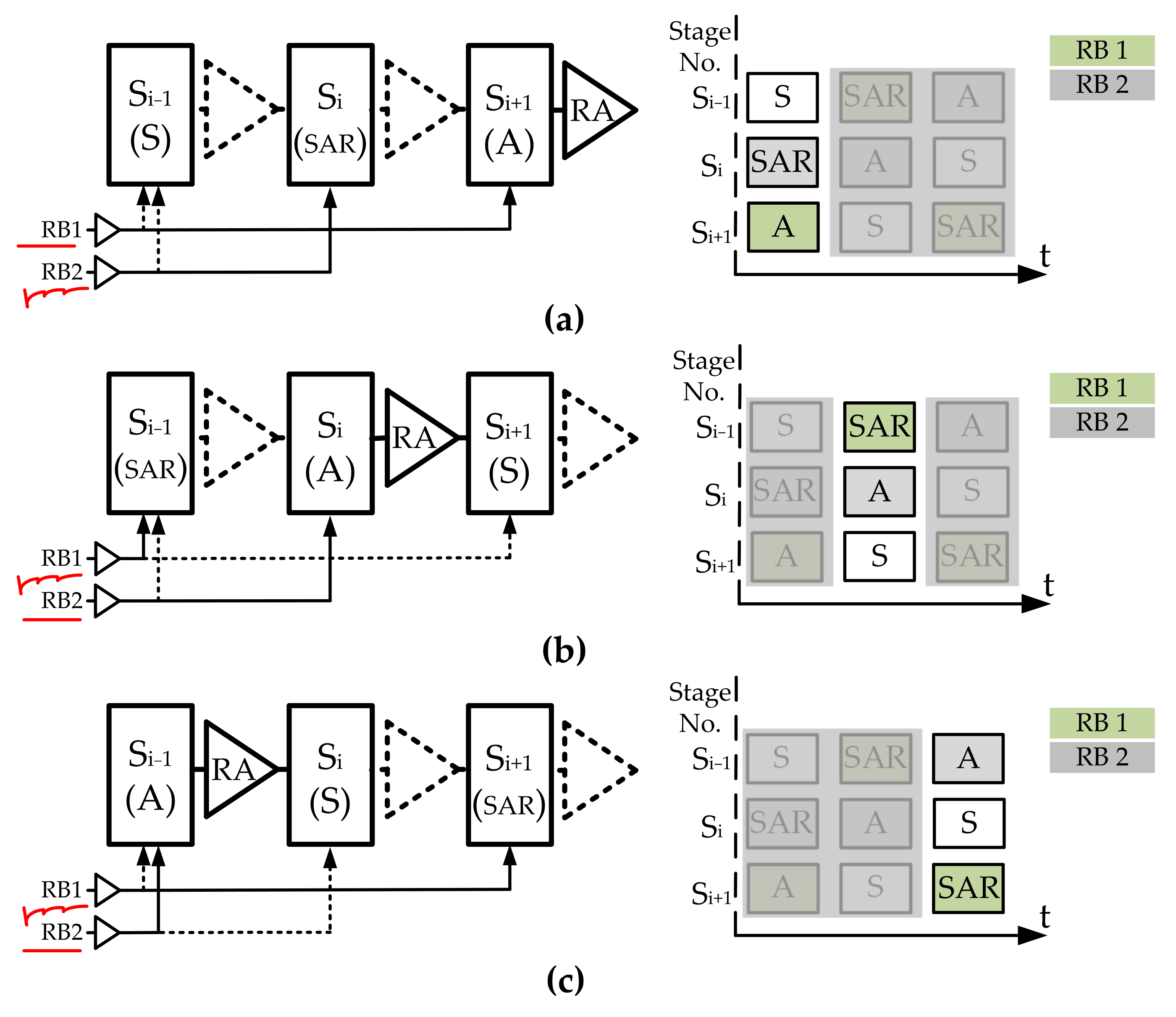
2. Reference and Op-Amp Sharing in Pipelined-SAR ADCs

2.1. Proposed Reference Sharing Scheme

Figure 4 shows the connections and the operating phases of the proposed reference sharing scheme between three adjacent pipeline stages (Si−1, Si, and Si+1). One-third of reference buffers are reduced with only a little extra cost of switches and no loss on performance. It is also compatible with the op-amp sharing technique similar to [28], which further improves the area-and-power efficiency. For simplicity, only single-ended circuits are drawn. RB1 and RB2 represent two independent reference buffers. The Sampling, SAR, and Amplification phases are designed to each take one-third of the operating cycle, which is easy to realize in medium-speed scenarios.
In phase (a), Si−1 is in the sampling phase, connected to input common-mode voltage (not drawn in the figure). And Si performs SAR conversion, drawing charge from RB2. Si+1 is connected to RB1 to hold the residual voltage. In the next phase (b), Si−1 is connected to RB1 for SAR conversion, and Si is connected to the idle RB2. The shared residual amplifier is connected between Si and Si+1. Si+1 is in the sampling phase. In the last phase (c), the residue voltage held by RB2 in Si−1 is amplified. Si samples while RB1 charges Si+1.
With this reference sharing scheme, only two pairs of references are alternately connected to any three adjacent pipeline stages. A reference buffer serves only one stage in SAR conversion, and an idle reference is always connected to the stage in the Amplification phase. Hence, the risk of decision error and gain error are eliminated.
Figure 5 compares the described scheme in (a) and an alternative implementation in (b). In Figure 5b, each stage connects to both reference buffers, thus fully mitigating the offset caused by mismatches between the references. Compared with (b), the connection of references in Figure 5a is much simpler, and the offset in Si−1 which is more critical, is also eased. In addition, in this scheme, RB2 is only used for Si charging, whose capacitance load is smaller than Si−1, as a result the power consumption of RB2 can be further reduced.

2.2. Op-Amp Sharing in the Proposed Scheme

In conventional pipelined ADCs, the primary concern of op-amp sharing is the memory effects that will degrade settlement accuracy and sampling rate. This problem worsens in pipelined-SAR ADCs because SAR conversion takes up extra time, resulting in less time available for the op-amp to reset. When applying the proposed scheme, this dilemma is alleviated because the settlement requirement of Si is less than that of Si−1, a part of the settlement time is saved and a reset phase can be inserted after phase (b). Besides, after phase (c) there is a long idle time (phase (a)) to completely eliminate the residual charge.
The op-amp can also be biased differently in phase (b) and (c) to reduce power consumption. The detailed timing diagram and circuit implementation are shown in Section 4 and Section 5.

3. Architecture Optimization Based on Reference/Op-Amp Sharing

As explained in Section 1, the area-and-power efficiency rather than sampling rate is more essential in the multi-channel ultrasound imaging system. Based on the reference/op-amp sharing scheme, the efficiency can be further improved by optimizing the number of stages and the stage resolution distribution. In this section, the effectiveness of sharing is first compared in different architectures. In order to better measure the design cost of these architectures, a unit capacitance-based analysis method which eliminates the impact introduced by the process and circuit design is explained. And finally, an optimized architecture is proposed for the 14-bit design target. Its superiority is demonstrated by comparison with other possible implementations.

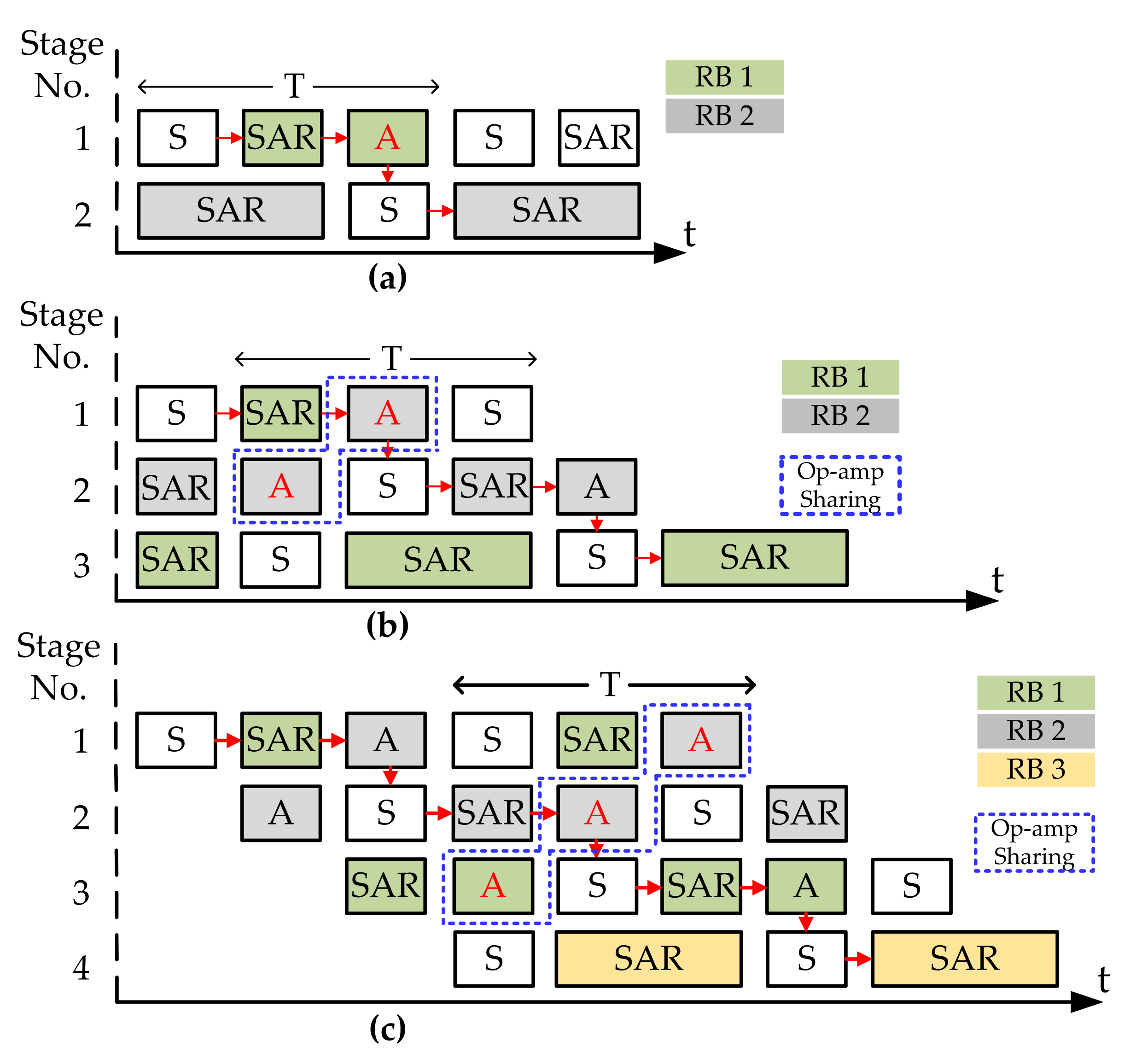
3.1. Reference and Op-Amp Sharing in Different Architectures

Figure 6 presents the timing diagram of three pipelined-SAR ADCs with a different number of stages. The application of sharing scheme is also illustrated. A two-stage pipelined-SAR ADC in (a) cannot share op-amp and reference. A four-stage pipelined-SAR ADC in (c) needs only a single op-amp, but three references are required, even with reference sharing. For a three-stage architecture in (b), the sharing scheme maximizes the efficiency with one op-amp and only two references are shared between stages. A detailed comparison of area and power consumption [29,30] of these pipelined-SAR ADCs is made in the following sections.

3.2. Principle of Area and Power Consumption Analysis

To focus on the optimization of architectures, it is necessary to exclude the offset brought by the process and circuit design, and then a fair comparison can be made. It is achieved by normalizing the design cost of area and power to the unit capacitor provided by each process. The principle is detailed presented as follows.

3.2.1. Area Analysis

The area of a pipelined-SAR ADC can be expressed as:
A t o t a l = i = 1 M A s t a g e , i + N o p × A o p + N r e f × A r e f
where Atotal, Astage,i, Aop, and Aref represent the area of an M-stage ADC, the i-th stage, the op-amp, and the reference (including decoupling capacitors), respectively. The number of amplifiers (Nop) and reference (Nref) can be reduced by reference/op-amp sharing.
Astage,i is composed of several unit capacitors (Aucap,i) and active parts (Aactive,i) in this stage, including comparators, SAR logic, and switches. The number of unit capacitors is exponentially related to the stage resolution (ki) and is modified by different switching schemes (usually 2 k i capacitors are needed). The unit capacitor in each stage may also scale down according to the linearity and noise requirement. And since the active parts drive the capacitors (ignoring the relatively small comparators), it is reasonable to assume that Aactive,i is proportional to the capacitance.
In Equation (2), the area of one stage is normalized to the unit capacitor (Aunit) provided by the process. α is the proportional coefficient between the size of capacitors and active parts, x is the scaling “taper factor” that is mostly around 2 [31], and γ is the ratio between unit capacitor used in the first stage and the unit capacitor provided by the process (Aucap,1/Aunit).
A s t a g e , i k i = 2 k i A u c a p , i + A a c t i v e , i = 1 + α 2 k i A u c a p , i = 1 + α x 1 i 2 k i γ A u n i t
Bringing Equation (2) into (1), Equation (3) shows that the overall area is determined by the stage resolution distribution (ki) and the number of op-amps (Nop) and references (Nref). The coefficients (α, x, γ) reflect the impact caused by the process and circuit design.
A t o t a l = i = 1 M 1 + α x 1 i 2 k i γ A u n i t + N o p × A o p + N r e f × A r e f

3.2.2. Power Consumption Analysis

The total power consumption (Ptotal) of an M-stage pipelined-SAR ADC is made up of switching power of capacitors in each stage (Pstage,i), power of residue amplifiers (Pop), and references (Pref), as listed in Equation (3).
P t o t a l = i = 1 M P s t a g e , i + N o p × P o p + N r e f × P r e f
For simplicity, the difference between the residue amplifier and the reference buffer of each stage due to scaling down is neglected.
Because the power consumption of each stage (Pstage,i) under a given sampling rate is also determined by unit capacitors and corresponding active parts, the expression is similar to the analysis of the area in Equation (2). Replacing Aunit with the switching power of a unit capacitor (Punit), the normalized Pstage,i is represented in Equation (5). And β is the proportional coefficient of active parts to the capacitors in each stage.
P s t a g e , i k i = 1 + β x 1 i 2 k i γ P u n i t
Combing Equations (4) and (5), the overall power consumption is also determined by ki, Nop and Nref, as shown in Equation (6).
P t o t a l = i = 1 M 1 + β x 1 i 2 k i γ P u n i t + N o p × P o p + N r e f × P r e f

3.3. Proposed Area-and-Power Efficient Three-Stage Architecture for a 14-Bit ADC

According to the discussion of the sharing effectiveness in Section 3.1, a three-stage architecture can maximally utilize the shared reference and op-amp (in other words, Nop and Nref are reduced). Thus, an area-and-power efficient three-stage architecture with optimized stage resolution distribution (ki) is proposed for ADCs with 14-bit resolution and medium sampling rate. The resolution of each stage is 5-bit, 5-bit, and 6-bit, respectively, with a 1-bit inter-stage redundancy.
Table 1 lists other designs that also achieve 14-bit resolution and a similar sampling rate with different stage resolution distributions. They also have a 1-bit inter-stage redundancy. For three- and four-stage architectures, the resolution of pipeline stages is set to be the same to reduce the complexity of timing. Each design’s area and power consumption are normalized to the unit capacitor in each process according to Equations (3) and (6). The area and power consumption of a single op-amp and reference (including the buffer and the decoupling capacitor) compared to the unit capacitor are listed in Table 2. It is based on the measurement results of these reference designs and statistical results in [23].
As shown in Figure 7, the superiority of the proposed architecture is demonstrated, achieving both the least normalized area and power. For all architectures, the area and power consumption of capacitors decrease with the increase of the number of stages. If with three or more stages, the op-amp and reference rather than capacitors dominate the design cost. Because of op-amp sharing, only a single op-amp is used in all of these architectures. The number of references becomes the key that distinguishes the three-stage from the four-stage architecture, where the three-stage architecture requires one less reference, saving significantly more area and power.
Between the two three-stage architectures, the proposed “5-5-6-bit” architecture balances the capacitance of each stage better, hence achieving better area-and-power efficiency than the other.

3.4. Summary of This Section

In this section, the effectiveness of reference/op-amp sharing is compared and a generic analysis method for the area and power consumption of pipelined-SAR ADCs is presented. Combing these two, a three-stage architecture with a “5-5-6-bit” stage resolution distribution is proposed. Its area-and-power efficiency is the best in comparison with other architectures, thus it is adopted in the targeted 14-bit 50 MS/s ADC design.

4. Proposed Three-Stage Pipelined-SAR ADC

4.1. Overall Structure
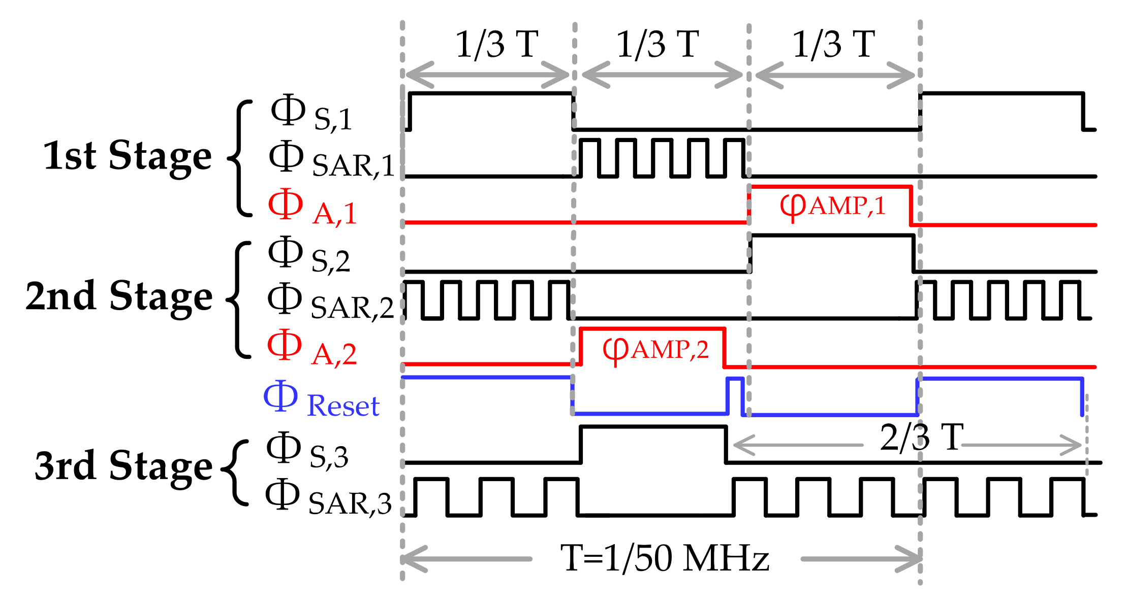
Figure 8 shows the overall structure of the proposed ADC. It consists of 16 independent sub-channel ADCs and peripheral circuits, including LVDS, serial peripheral interface (SPI), bandgap, phase-locked loop (PLL). Each sub-channel ADC realizes a 14-bit resolution with a 50 MS/s sampling rate, and the quantization results are converted into serial output by LVDS. A 50-MHz frame clock (FCO) and a 700-MHz data clock (DCO) are also outputted.
The main part of each sub-channel ADC is a three-stage pipelined-SAR ADC with a “5-5-6-bit” resolution distribution. There is 1-bit redundancy between each stage to eliminate the risk of an overflow caused by comparators’ offset, and a taper factor of 1.4 is applied in the unit capacitance. The sub-ADCs of the first two stages are asynchronous. The residual voltage of each stage is amplified 16 times through a shared op-amp. The third stage uses synchronous timing SAR logic to finish the left 6-bit quantization. The outputs of three stages are added in ADDer, where the least significant bit (LSB) of the former stage overlaps with the most significant bit (MSB) of the latter stage, generating the final 14 bits output. Each sub-channel ADC has its own reference, guaranteeing it is not affected by adjacent channels.

4.2. Timing Diagram

The detailed timing diagram of the proposed ADC is shown in Figure 9. In the first and second stage, each Sampling, SAR, and Amplification phase takes roughly one-third of the cycle. After sampling, the asynchronous SAR ADC finishes five trials, and then the shared op-amp starts to work in the two adjacent phases (φAMP,1 and φAMP,2). Due to the relaxed settlement requirement, φAMP,2 is a little shorter than φAMP,1, and a quick reset phase (0.6 ns) is inserted between them. The third stage has a longer time for SAR conversion. Therefore, a simple and robust synchronous timing logic is adopted, generating the last six bits.

5. Circuit Implementation

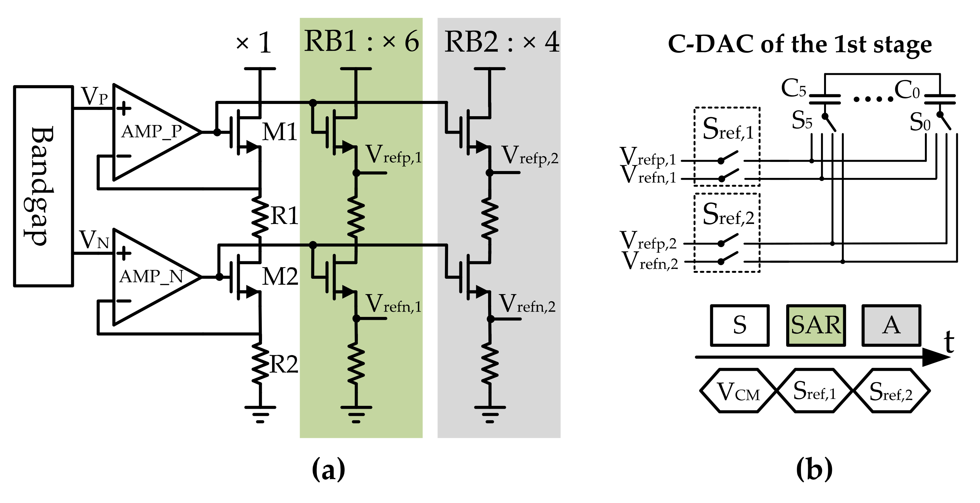
5.1. Shared Reference
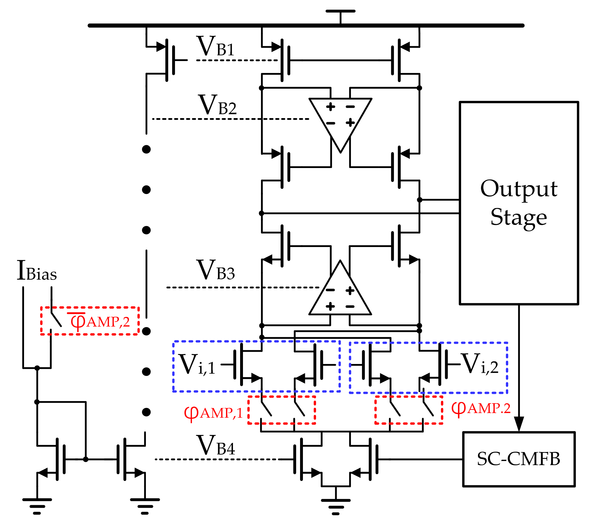
The shared reference in this design is shown in Figure 10. Figure 10a shows the circuit implementation, where a master-slave architecture is adopted, consisting of a feedback loop and two open-loop buffer branches. The common-mode voltage (Vcm) is also generated by a similar branch and is neglected for simplicity. All of the source followers are composed of NMOS transistors, which are more efficient in converting current to transconductance (gm/ID) than PMOS transistors, thus reducing power consumption and parasitic introduced by the transistors [34].
In the feedback loop, the two error amplifiers with different input pairs are biased in the subthreshold region to save power. M1, M2, and R1, R2 determine the operation point of the buffer branches.
The driving capability of the branches is designed differently according to the discussion in Section 2.2. The settlement requirement of RB2 is eased since it only needs to charge the second stage. The number of branches is reduced accordingly.
Figure 10b shows the circuit implementation and the operation phases of reference sharing in the C-DAC of the first stage. Each capacitor connects to both references through two pairs of switches (Sref,1 and Sref,2). During the SAR phase, Sref,1 is close with Sref,2 open and RB1 charges the C-DAC. Then in the Amplification phase, Sref,1 is open with Sref,2 close, and RB2 provides the idle reference to hold the residue voltage.

5.2. Shared Op-Amp

In this design, the shared op-amp adopts a two-stage Miller-compensated architecture with high PVT robustness (Figure 11). The output stage uses a push–pull architecture with switched-capacitor common-mode feedback (SC-CMFB), whose details are omitted in the figure for simplicity. The amplifier achieves a gain-bandwidth product (GBW) of 2.8 Giga with 118.7-dB dc gain and 65° phase margin when operating for the first stage.
To reduce the memory effect, the amplifier uses two independent input pairs (Vi,1 and Vi,2) for the first and second Amplification phase (φAMP,1 and φAMP,2). During the reset phase described in Section 4.2, both pairs of input transistors are connected to the input common-mode voltage to eliminate the residual charge.
To further reduce power consumption, the op-amp uses an adjustable bias. Since the load capacitance is smaller and the settlement requirement is eased in the second Amplification phase, the quiescent operating current of the op-amp can be reduced. It is realized by reducing the bias current inputted to the bias network, thus changing the DC operating points in the op-amp. In this way, 25% of the power consumption is reduced, and the GBW is reduced to 2 Giga with 72° phase margin.

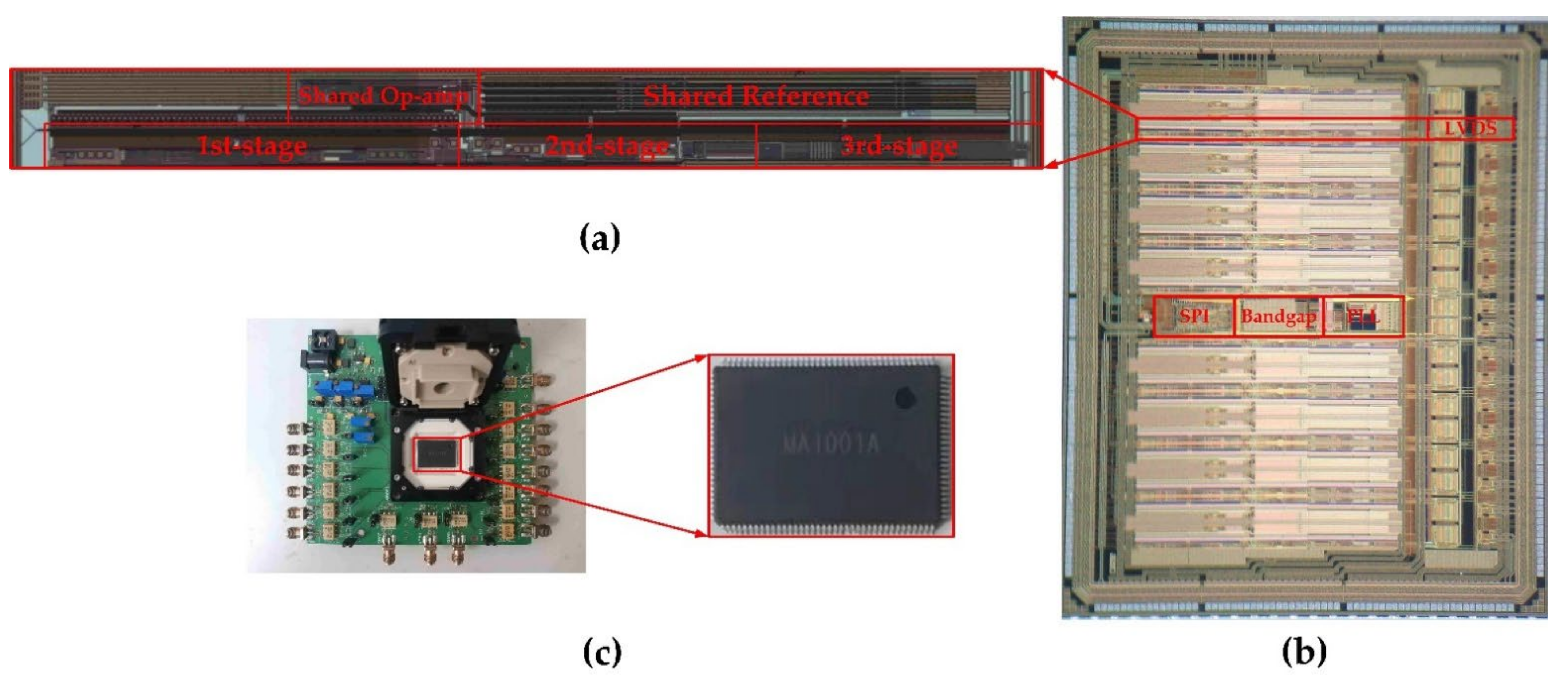
5.3. Layout Considerations

Since it is necessary to integrate 16 channels of the proposed ADC in a single die, the overall floorplan needs to be fully considered during the top-level design. Considering the high design and testing cost of the ball grid array (BGA) package, a quad flat package (QFP) package is adopted with its pins laid around the package. Accordingly, each channel of the ADC is designed as a slim rectangle to place the input/output pins on the left and right sides of the package, and the 16 channels are lined up in a row. Due to the elongated shape, the distance between each stage is stretched. Especially when the reference sharing scheme is applied, RB1 needs to connect both the first and third stages, running through the entire chip. Therefore, the parasitic capacitance and resistance introduced by wiring are carefully simulated to minimize the RC time constant and to prevent settlement errors. In addition, the LVDS of all channels share the same clock, so the clock distribution network of the PLL is also balanced to ensure a consistent clock phase. Finally, the supply network is simulated and verified by electromigration analysis.

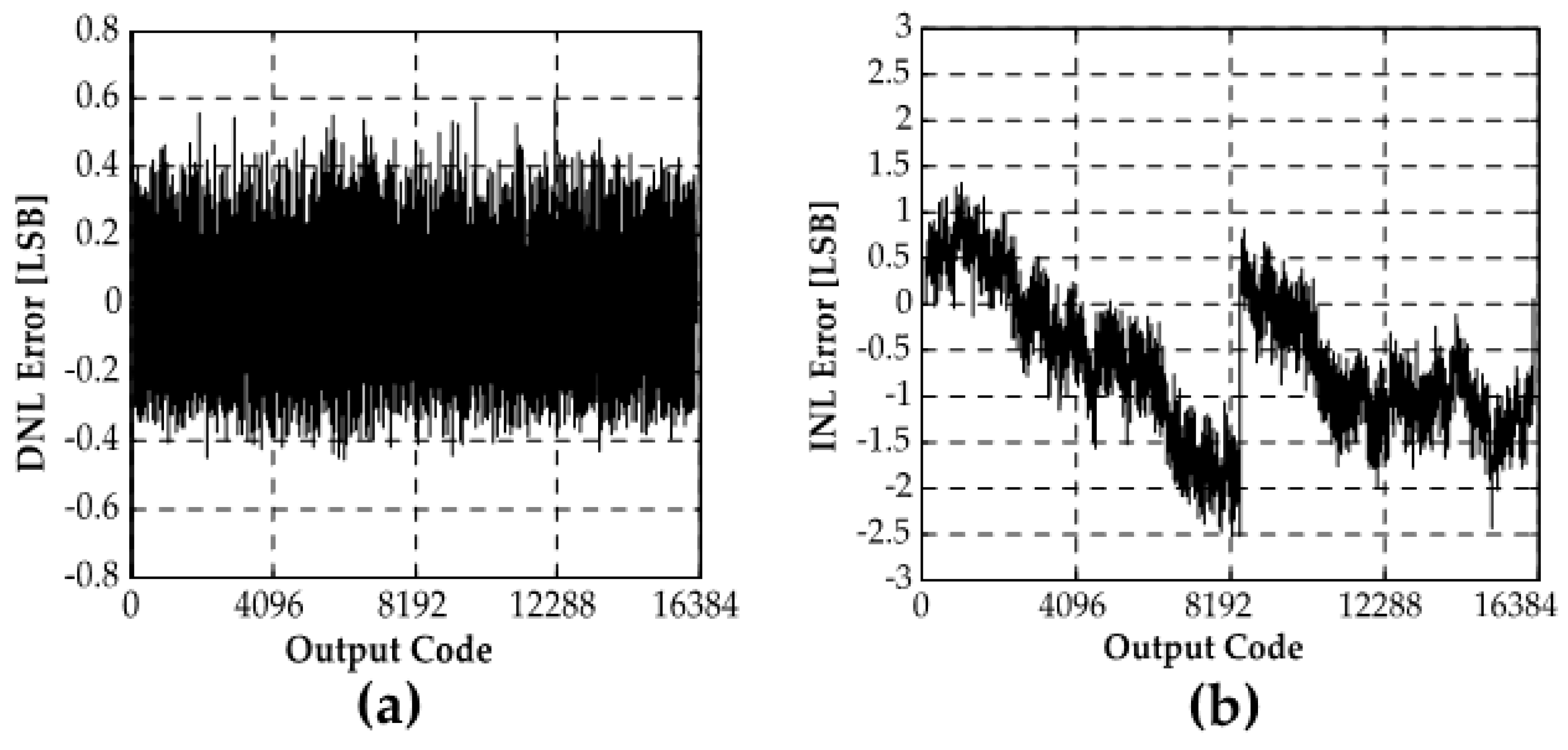
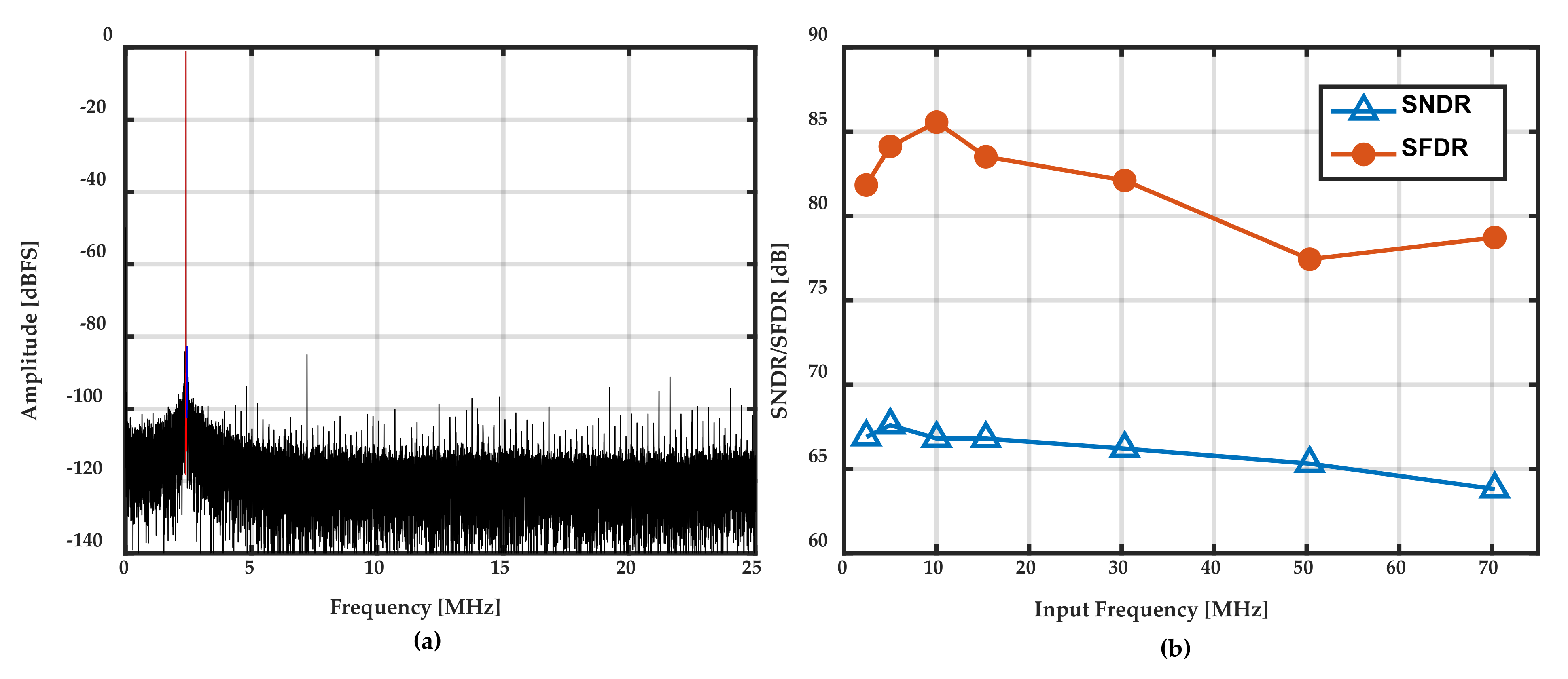
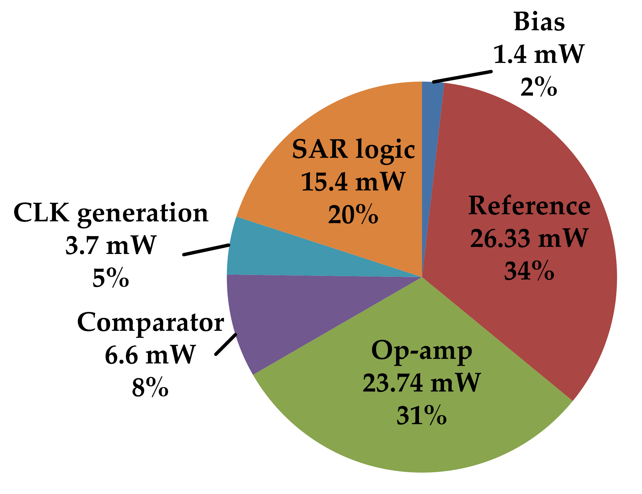
6. Measurement Results

Figure 12a shows the photograph of the proposed single-channel ADC, where each circuit block is designed as a long skinny rectangle. The shared op-amp and reference are beside the three stages. The area of the single-channel ADC is 2 mm × 0.25 mm. Figure 12b shows the photograph of the whole chip. SPI, bandgap, and PLL locate between the top and bottom eight channels. Figure 12c is the packaged chip and the socket test board for batch testing.
Figure 13 shows the measured static performance. The test is done with a 2.4-MHz sinusoidal input signal and 50-MHz sampling frequency under a 1.8-V supply. The measurement result is analyzed by code density, and the calculated differential nonlinearity (DNL) error and integral nonlinearity (INL) error is −0.46/0.6 LSB and −2.53/1.32 LSB, respectively.
Figure 14a. shows a typical dynamic performance of the ADC, achieving an SFDR of 82.19 dB, and an SNDR of 68.25 dB at 2.4-MHz input. Figure 14b shows the measured dynamic performance versus input frequency up to 70 MHz. This ADC maintains stable SFDR and SNDR performance in the second Nyquist zone, making it suitable for second harmonic ultrasound imaging. And the performance is uniform for different channels with a 1.9 dB standard deviation of SNDR among more than 50 test chips. It is also tested from −30 to 80 °C with only slight performance loss.
When integrating the 16 channels, each channel is surrounded by guard rings. Sensitive signals are also protected by shield wires. The measured crosstalk coefficient between two adjacent channels is −65 dB and slightly changed under different input frequencies, which are mainly introduced by bonding wires and the testing board.
The power breakthrough of a single channel is shown in Figure 15. All other peripheral circuits consume 12 mW/channel on average. The core consumes 49.5 mW (references not included), translating into an FoM of 0.47 pJ/conversion-step. Though limited by the process which leads to high total power consumption, the effectiveness of reference sharing is verified with 15% power saved. The three-stage pipelined-SAR architecture combing both reference and op-amp sharing scheme achieves an estimated 30% power reduction, showing great potential in further applications.
Table 3 summarizes the performance and compares it with other ADCs. Compared with ADCs with 14-bit resolution and similar sampling rate [32,35,36], the proposed ADC integrates more channels in a single chip and achieves a comparable SNDR performance without any calibration. The area efficiency is demonstrated especially compared to [36], which is also designed in a 0.18-μm process. And compared with the ADCs reported for ultrasound imaging systems [37,38], the proposed ADC achieves higher resolution and a competitive FoM.

7. Conclusions

In this paper, a reference sharing scheme that is suitable for medium-speed, high-resolution, pipelined-SAR ADC is proposed. Based on this, a three-stage architecture with reference/op-amp sharing and optimized stage resolution distribution is proposed and verified. A prototype 16-channel ADC is designed and measured in a 0.18-μm process with 14-bit resolution and a 50-MS/s sampling rate. The measurement results show that the proposed architecture can save up to 30% power with no cost to performance, achieving high area-and-power efficiency, which is suitable for ultrasound imaging systems.

Author Contributions

Conceptualization, Y.W.; methodology, Y.W.; validation, Y.W.; formal analysis, Y.W.; writing—original draft preparation, Y.W.; supervision, F.Y.; project administration, J.R. All authors have read and agreed to the published version of the manuscript.

Funding

This work is supported by National Key Research and Development Project with a grant number of 2020YFC0122100.

Data Availability Statement

Data is contained within the article. The data presented in this study are available in this paper.

Conflicts of Interest

The authors declare no conflict of interest.

References

  1. Tang, H.; Lu, Y.; Assaderaghi, F.; Daneman, M.; Jiang, X.; Lim, M.; Ng, E.; Singhal, U.; Tsai, J.M. 3D Ultrasonic Fingerprint Capacitive Fingerprint Sensor. In Proceedings of the IEEE International Solid-State Circuits Conference, San Francisco, CA, USA, 31 January 2016. [Google Scholar]
  2. Chen, M.-C.; Perez, A.P.; Kothapalli, S.-R.; Cathelin, P.; Cathelin, A.; Gambhir, S.S.; Murmann, B. A Pixel Pitch-Matched Ultrasound Receiver for 3-D Photoacoustic Imaging With Integrated Delta-Sigma Beamformer in 28-nm UTBB FD-SOI. IEEE J. Solid-State Circuits 2017, 52, 1–14. [Google Scholar] [CrossRef] [PubMed]
  3. Romero-Morales, C.; Martín-Llantino, P.; Calvo-Lobo, C.; San-Antolín, M.; López-López, D.; Blanco-Morales, M.; Rodríguez-Sanz, D. Ultrasound Imaging of the Abdominal Wall and Trunk Muscles in Patients with Achilles Tendinopathy versus Healthy Participants. Diagnostics 2019, 10, 17. [Google Scholar] [CrossRef] [Green Version]
  4. Petrusca, L.; Varray, F.; Souchon, R.; Bernard, A.; Chapelon, J.Y.; Liebgott, H.; N’Djin, W.A.; Viallon, M. Fast Volumetric Ultrasound B-Mode and Doppler Imaging with a New High-Channels Density Platform for Advanced 4D Cardiac Imaging/Therapy. Appl. Sci. 2018, 8, 200. [Google Scholar] [CrossRef] [Green Version]
  5. Liu, H.-L.; Jan, C.-K.; Chu, P.-C.; Hong, J.-C.; Lee, P.-Y.; Hsu, J.-D.; Lin, C.-C.; Huang, C.-Y.; Chen, P.-Y.; Wei, K.-C. Design and Experimental Evaluation of a 256-Channel Dual-Frequency Ultrasound Phased-Array System for Transcranial Blood–Brain Barrier Opening and Brain Drug Delivery. IEEE Trans. Biomed. Eng. 2014, 61, 1350–1360. [Google Scholar] [CrossRef]
  6. Chen, D.; Cui, X.; Zhang, Q.; Li, D.; Cheng, W.; Fei, C.; Yang, Y. A Survey on Analog-to-Digital Converter Integrated Circuits for Miniaturized High Resolution Ultrasonic Imaging System. Micromachines 2022, 13, 114. [Google Scholar] [CrossRef] [PubMed]
  7. Analog Devices Inc. Octal LNA/VGA/AAF/ADC and Crosspoint Switch. AD9272 Datasheet, April 2009, revised July 2017. Available online: https://www.analog.com/media/en/technical-documentation/data-sheets/AD9272.pdf (accessed on 23 February 2022).
  8. Texas Instruments. 16-Channel Ultrasound AFE with 90-mW/Channel Power, 1-nV/√Hz Noise, 14-Bit, 65-MSPS or 12-Bit, 80-MSPS ADC and Passive CW Mixer; AFE5816 Datasheet, April 2015, revised September 2017. Available online: https://www.ti.com/lit/ds/symlink/afe5816.pdf (accessed on 23 February 2022).
  9. Analog Devices Inc. Octal Ultrasound AFE with JESD204B. AD9675 Datasheet. January 2016. Available online: https://www.analog.com/media/en/technical-documentation/data-sheets/AD9675.pdf (accessed on 24 February 2022).
  10. Lagos, J.; Markulic, N.; Hershberg, B.; Dermit, D.; Shrivas, M.; Martens, E.; Craninckx, J. A 10.1-ENOB, 6.2-fJ/conv.-step, 500-MS/s, Ringamp-Based Pipelined-SAR ADC With Background Calibration and Dynamic Reference Regulation in 16-nm CMOS. IEEE J. Solid-State Circuits 2022, 1. [Google Scholar] [CrossRef]
  11. Lan, J.; Zhai, D.; Chen, Y.; Ni, Z.; Shen, X.; Ye, F.; Ren, J. A 2.5-GS/s Four-Way-Interleaved Ringamp-Based Pipelined-SAR ADC with Digital Background Calibration in 28-nm CMOS. Electronics 2021, 10, 3173. [Google Scholar] [CrossRef]
  12. Malki, B.; Verbruggen, B.; Wambacq, P.; Deguchi, K.; Iriguchi, M.; Craninckx, J. A Complementary Dynamic Residue Amplifier for a 67 dB SNDR 1.36 mW 170 MS/s Pipelined SAR ADC. In Proceedings of the European Solid-State Circuits Conference, Venezia Lido, Italy, 22 September 2014. [Google Scholar]
  13. Kwon, Y.; Kim, T.; Sun, N.; Chae, Y. A 348-μW 68.8-dB SNDR 20-MS/s Pipelined SAR ADC With a Closed-Loop Two-Stage Dynamic Amplifier. IEEE Solid-State Circuits Lett. 2021, 4, 166–169. [Google Scholar] [CrossRef]
  14. Ni, M.; Wang, X.; Li, F.; Wang, Z. A 13-bit 312.5-MS/s Pipelined SAR ADC With Open-Loop Integrator-Based Residue Amplifier and Gain-Stabilized Integration Time Generation. IEEE Trans. Very Large Scale Integr. (VLSI) Syst. 2021, 29, 1416–1427. [Google Scholar] [CrossRef]
  15. Wu, C.; Yuan, J. A 12-Bit, 300-MS/s Single-Channel Pipelined-SAR ADC with an Open-Loop MDAC. IEEE J. Solid-State Circuits 2019, 54, 1446–1454. [Google Scholar] [CrossRef]
  16. Lee, C.C.; Flynn, M.P. A SAR-Assisted Two-Stage Pipeline ADC. IEEE J. Solid-State Circuits 2011, 46, 859–869. [Google Scholar] [CrossRef]
  17. Lien, Y.-C. A 14.6 mW 12 b 800 MS/s 4×time-interleaved pipelined SAR ADC achieving 60.8 dB SNDR with Nyquist input and sampling timing skew of 60 fsrms without calibration. IEEE Symp. 2016, 1–2. [Google Scholar] [CrossRef]
  18. Chen, L.; Sanyal, A.; Ma, J.; Sun, N. A 24-mW 11-Bit 1-MS/s SAR ADC with a Bidirectional Single-Side Switching Technique. In Proceedings of the European Solid-State Circuits Conference, Venezia Lido, Italy, 22 September 2014. [Google Scholar]
  19. Ginsburg, B.P.; Chandrakasan, A.P. An Energy-Efficient Charge Recycling Approach for a SAR Converter with Capacitive DAC. In Proceedings of the IEEE International Symposium on Circuits and Systems, New York, NY, USA, 23 May 2005. [Google Scholar]
  20. Zhu, Y.; Chan, C.-H.; Chio, U.-F.; Sin, S.-W.; Seng-Pan, U.; Martins, R.P.; Maloberti, F. A 10-bit 100-MS/s Reference-Free SAR ADC in 90 nm CMOS. IEEE J. Solid-State Circuits 2010, 45, 1111–1121. [Google Scholar] [CrossRef]
  21. Liu, C.C.; Chang, S.J.; Huang, G.Y.; Lin, Y.Z.; Huang, C.M.; Huang, C.H.; Bu, L.; Tsai, C.C. A 10 b 100 MS/s 1.13 mW SAR ADC with Binary-Scaled Error Compensation. In Proceedings of the IEEE International Solid-State Circuits Conference, San Francisco, CA, USA, 7 February 2010. [Google Scholar]
  22. Cao, Y.; Zhang, S.; Zhang, T.; Chen, Y.; Zhao, Y.; Chen, C.; Ye, F.; Ren, J. A 91.0-dB SFDR Single-Coarse Dual-Fine Pipe-lined-SAR ADC with Split-Based Background Calibration in 28-nm CMOS. IEEE Trans. Circuits Syst. I Regul. Pap. 2021, 68, 641–654. [Google Scholar] [CrossRef]
  23. Li, C.; Chan, C.-H.; Zhu, Y.; Martins, R.P. Analysis of Reference Error in High-Speed SAR ADCs with Capacitive DAC. IEEE Trans. Circuits Syst. I Regul. Pap. 2018, 66, 82–93. [Google Scholar] [CrossRef]
  24. Ju, H.; Lee, S.; Lee, M. A 12-bit 40-MS/s SAR ADC with Calibration-Less Switched Capacitive Reference Driver. Electronics 2020, 9, 1854. [Google Scholar] [CrossRef]
  25. Harikumar, P.; Wikner, J.J. Design of a Reference Voltage Buffer for a 10-Bit 50 MS/s SAR ADC in 65 nm CMOS. In Proceedings of the IEEE International Symposium on Circuits and Systems, Lisbon, Portugal, 24 May 2015. [Google Scholar]
  26. Shehzad, K.; Verma, D.; Khan, D.; Ain, Q.U.; Basim, M.; Kim, S.J.; Pu, Y.; Hwang, K.C.; Yang, Y.; Lee, K.-Y. Design of a Low Power 10-b 8-MS/s Asynchronous SAR ADC with On-Chip Reference Voltage Generator. Electronics 2020, 9, 872. [Google Scholar] [CrossRef]
  27. Jeon, Y.-D.; Nam, J.-W.; Kim, K.-D.; Roh, T.M.; Kwon, J.-K. A Dual-Channel Pipelined ADC with Sub-ADC Based on Flash–SAR Architecture. IEEE Trans. Circuits Syst. II Express Briefs 2012, 59, 741–745. [Google Scholar] [CrossRef]
  28. Lee, K.H.; Kim, K.S.; Lee, S.H. A 12 b 50 MS/s 21.6 mW 0.18 μm CMOS ADC Maximally Sharing Capacitors and Op-Amps. IEEE Trans. Circuits Syst. I Regul. Pap. 2011, 58, 2127–2136. [Google Scholar]
  29. Sun, L.; Ko, C.T.; Pun, K.P. Optimizing the Stage Resolution in Pipelined SAR ADCs for High-Speed High-Resolution Appli-cations. IEEE Trans. Circuits Syst. II Express Briefs 2014, 61, 476–480. [Google Scholar] [CrossRef]
  30. Wu, Y.; Lan, J.; Chen, M.; Ye, F.; Ren, J. A 16-channel 50MS/s 14bit Pipelined-SAR ADC for Integrated Ultrasound Imaging Systems. In Proceedings of the 2020 IEEE Asia Pacific Conference on Circuits and Systems (APCCAS), Ha Long, Vietnam, 8–10 December 2020; pp. 3–6. [Google Scholar] [CrossRef]
  31. Chiu, Y.; Gray, P.; Nikolic, B. A 14-b 12-MS/s CMOS pipeline ADC with over 100-dB SFDR. IEEE J. Solid-State Circuits 2004, 39, 2139–2151. [Google Scholar] [CrossRef]
  32. Xu, H.; Member, S.; Huang, H.; Cai, Y.; Du, L.; Zhou, Y.; Member, S. A 78.5-dB SNDR Radiation- and Metastability- Tolerant Two-Step Split SAR ADC Operating Up to 75 MS/s with 24.9-mW Power Consumption in 65-nm CMOS. IEEE J. Solid-State Circuits 2019, 54, 441–451. [Google Scholar] [CrossRef]
  33. Wang, R.; Chio, U.-F.; Sin, S.-W.; Seng-Pan, U.; Wang, Z.; Martins, R.P. A 12-bit 110MS/s 4-stage single-opamp pipelined SAR ADC with ratio-based GEC technique. In Proceedings of the European Solid-State Circuits Conference, Bordeaux, France, 17 September 2012; pp. 265–268. [Google Scholar]
  34. Zheng, X.; Wang, Z.; Li, F.; Zhao, F.; Yue, S.; Zhang, C.; Wang, Z. A 14-bit 250 MS/s IF Sampling Pipelined ADC in 180 nm CMOS Process. IEEE Trans. Circuits Syst. I Regul. Pap. 2016, 63, 1381–1392. [Google Scholar] [CrossRef] [Green Version]
  35. Mao, J.; Guo, M.; Sin, S.-W.; Martins, R.P. A 14-Bit Split-Pipeline ADC with Self-Adjusted Opamp-Sharing Duty-Cycle and Bias Current. IEEE Trans. Circuits Syst. II Express Briefs 2018, 65, 1380–1384. [Google Scholar] [CrossRef]
  36. Miyahara, Y.; Sano, M.; Koyama, K.; Suzuki, T.; Hamashita, K.; Song, B.-S. A 14b 60 MS/s Pipelined ADC Adaptively Cancelling Opamp Gain and Nonlinearity. IEEE J. Solid-State Circuits 2013, 49, 416–425. [Google Scholar] [CrossRef]
  37. Kim, T.; Shin, S.; Kim, S. An 80.2 dB DR 23.25 mW/Channel 8-Channel Ultrasound Receiver with a Beamforming Embedded SAR ADC. IEEE Trans. Circuits Syst. II Express Briefs 2018, 66, 1487–1491. [Google Scholar] [CrossRef]
  38. Chirala, M.K.; Huynh, P.; Ryu, J.; Kim, Y.H. A 128-ch Δ-Σ ADC Based Mixed Signal IC for Full Digital Beamforming Wireless Handheld Ultrasound Imaging System. In Proceedings of the Annual International Conference of the IEEE Engineering in Medicine and Biology Society, Milan, Italy, 25 August 2015. [Google Scholar]
Figure 1. System diagram of an ultrasound imaging system. The arrows indicate the electronic signal flow in both Tx and Rx channels. Components surrounded by a dashed box are usually integrated into a single chip. A multi-channel ADC quantifies signals from multiple chips and sends them to FPGA.
Electronics 11 00749 g001
Figure 2. Block diagram of a pipelined-SAR ADC. The area marked with grey represents the critical blocks in the i-th stage. The detailed structure of the C-DAC, including capacitor array and sampling switch, is in the dashed box. A simplified timing diagram is drawn below.
Electronics 11 00749 g002
Figure 3. Transient waveforms of the residual voltage and the output of the reference buffer in one stage of a pipelined-SAR ADC. The red line indicates the situation with no independent RB, which has a larger droop in the SAR phase and unwanted function during amplification, causing possible decision error and gain error, respectively.
Electronics 11 00749 g003
Figure 4. The phases and the connection of the reference sharing scheme along with op-amp sharing. Two reference buffers are connected to three adjacent stages (left). The solid and dotted lines represent the alternately connected paths. The current phase is highlighted in the timing diagram of each stage (right). The connected buffers are marked with green and grey. (a) RB1 idle, RB2 charging Si; (b) RB1 charging Si−1, RB2 idle; (c) RB1 charging Si+1, RB2 idle.
Electronics 11 00749 g004
Figure 5. Two possible implements of the reference sharing scheme. The connection differs in the Si and Si+1 where (a) references not exchanged and (b) references exchanged with each other.
Electronics 11 00749 g005
Figure 6. The timing diagram of pipelined-SAR ADCs with (a) two stages, (b) three stages, and (c) four stages. In each timing diagram, the signal flow is represented with red arrows. The blue dashed box means that the amplification in different phases is finished with a shared op-amp. The needed reference buffer is marked with different colors.
Electronics 11 00749 g006
Figure 7. Comparison of area and power between different architectures. Each component in the stacked bar is marked with different colors and grains, as illustrated below. The normalized area and power are compared in left and right, respectively. The trend lines of the sum area (blue) and power (brown) indicate that the architecture in this work achieves the best efficiency.
Electronics 11 00749 g007
Figure 8. The overall structure of the proposed ADC. The ADC has 16 channels and each channel is drawn in the solid line box, including three sub-stages, the shared reference/op-amp and LVDS. The peripheral circuits shared by all channels are drawn below. As illustrated right, different signal flows are marked with arrows with different colors.
Electronics 11 00749 g008
Figure 9. The timing diagram of the proposed ADC. The detailed phase clock of each stage is grouped. The shared op-amp has two operating phases (red line), and the Reset phase (blue line) is inserted between them. The Sampling, SAR, and Amplification phases each take one-third of the period.
Electronics 11 00749 g009
Figure 10. (a) The circuit implementation of the shared reference. The feedback loop with error amplifiers is on the left. Two references are marked with different colors. The number of branches is also annotated. (b) Implementation of the reference sharing in the 1st stage. The two pairs of switches for sharing are in the dashed box. The corresponding timing diagram is also drawn below, where Sref,1 is connected in the SAR phase and Sref,2 in the Amplification phase.
Electronics 11 00749 g010
Figure 11. The shared op-amp with adjustable bias. The two input pairs for different inputs are in the blue dashed box, along with their control switches in the red box. When operating for the 2nd stage, the switch on IBias (left) is open, reducing the overall bias current and saving power.
Electronics 11 00749 g011
Figure 12. Photograph of (a) single-channel ADC, with main blocks marked in the red box; (b) 16-channel ADC with peripheral circuits integrated, which are also annotated; and (c) package and the batch test board with a socket.
Electronics 11 00749 g012
Figure 13. Measured (a) DNL error and (b) INL error. The DNL error and INL error is −0.46/0.6 LSB and −2.53/1.32 LSB, respectively. They are calculated from a histogram test with full-swing input and 16,384 sampling points.
Electronics 11 00749 g013
Figure 14. (a) Measured output amplitude in the spectrum with 2.4-MHz input, achieving an SFDR of 82.19 dB, and an SNDR of 68.25 dB; (b) dynamic performance versus input frequency. The SNDR is drawn in blue and SFDR in red. Used test frequencies are also marked with points and triangles.
Electronics 11 00749 g014
Figure 15. Power breakthrough of the proposed ADC. The power consumption of each block is annotated with its percentage. With the reference/op-amp sharing, 30% power is saved from the reference and op-amp, which are the most power-hungry blocks.
Electronics 11 00749 g015
Table 1. Comparison between architectures.
ArchitectureResolution
Distribution (ki) *
Case No.Number of Op-Amp (Nop)Number of References (Nref)
OriginalWith Op-amp SharingOriginalWith Reference Sharing
2-stage
PPL-SAR
6b + 9b [32]i1122
7b + 8b [21]ii1122
3-stage
PPL-SAR
4b + 4b + 8biii2132
5b + 5b + 6b (this work)iv2132
4-stage
PPL-SAR
4b × 3 + 5b [33]v3143
* The circuit-design and process-related coefficients (α, β, x, γ) will change the absolute values of area and power consumption, but not the relative relationships in the comparison. They are set based on the used 0.18-μm process as follows: α is 0.5, β is 0.2, x is 1.4. γ is mainly determined by the linearity of capacitors and is set to 2.
Table 2. Ranges of the area and power normalized to the unit capacitor.
Circuit BlockRange of Area (A/Aunit)Range of Power (P/Punit)
Residue Amplifier *100–40010–200
Reference *200–400100–500
* For simplicity, the median of the range is used, and the result is not changed by the value chosen.
Table 3. Performance summary and comparison.
[32][35][36][37][38]This Work
Technology65 nm65 nm180 nm180 nm130 nm180 nm
ArchitecturePipelined-SARSplit-PipelinePipelineSARSigma-DeltaPipelined-SAR
Number of Channels111812816
Sampling Rate (MS/s)7510060202050
Resolution (bit)141414121214
SNDR (dB)77.868.576.958.26568.25
SFDR (dB)92.184.491.2N/A5882.19
Power/channel a (mW)24.93267.82.61749.5
Area/channel (mm2)0.342 b0.381.430.26N/A0.625 b
FoM c (pJ/conv-step)0.0520.1470.1980.1960.5850.469
CalibrationBackgroundBackgroundBackground
LMS
Beam-
forming
BackgroundNot
required
a Core power consumption. b With on-chip reference buffer. c Walden FoM = Power/(2ENOB × Fs).
Publisher’s Note: MDPI stays neutral with regard to jurisdictional claims in published maps and institutional affiliations.

