Abstract
In this paper, we propose a bus-independent hardware (HW)-based approach to secure long protocol data units (PDUs) in Automotive Open System Architecture (AUTOSAR)-based automotive electronic control units (ECUs). Our approach is based on extending previous works that implemented two AUTOSAR communication (COM) application-specific instruction set processors (ASIPs). COM ASIP V1 introduced two instructions to handle the transmission and reception of PDUs no larger than 8 bytes and signals no larger than 32 bits individually through send signal and receive signal instructions. COM ASIP V2 introduced two extra instructions to handle long signals and PDUs of arbitrary lengths. We extended the instruction set architecture (ISA) of our previous ASIPs by introducing six new instructions, in COM ASIP V3, to hash PDUs that contain these signals to authenticate transmission and reception of such PDUs. The experimental results show that COM ASIP V3 can handle (i.e., transmit, receive, calculate hash, or verify hash) a 64-byte controller area network flexible data-rate (CAN FD) frame in and a 254-byte FlexRay frame in . These measurements indicate that the throughput of our new COM ASIP is much higher, 42× to 75×, than the throughput required by these communication buses.
1. Introduction
New communication buses (CAN FD [1,2], FlexRay [3,4,5], Ethernet, etc.) can transmit frames of longer lengths compared to traditional communication buses (CAN [6] and Local Interconnect Network (LIN)). These traditional communication buses are able to handle frames no larger than 8 bytes, whereas CAN FD can transmit frames of up to 64 bytes, FlexRay can transmit frames of up to 254 bytes, and Ethernet can transmit frames of up to 1518 bytes. These long frames contain many pieces of information. In some scenarios, it is needed to ensure the authenticity of these frames and make sure they will not be altered by attackers. In the context of AUTOSAR layered architecture [7], these frames are represented by PDUs in the Com module [8], and pieces of information inside PDUs are represented by signals in the Com module.
Our approach is based on extending previous works that implemented two AUTOSAR COM ASIPs. The first COM ASIP (i.e., COM ASIP V1) [9,10,11], as shown in Figure 1, introduced two instructions to handle transmission and reception of PDUs up to 8 bytes in length. This is done by handling signals no larger than 32 bits individually, inside these PDUs either by packing them during PDU transmission (i.e., through send signal instructions) or by unpacking them during PDU reception (i.e., through receive signal instructions). The second COM ASIP (i.e., COM ASIP V2) [12] introduced two extra instructions (i.e., the send long signal instruction and the receive long signal instruction) to handle long signals and PDUs of arbitrary lengths. The additions to COM ASIP V1 to support the long signal instructions are shown in Figure 2.
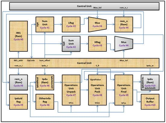
Figure 1.
COM ASIP V1.
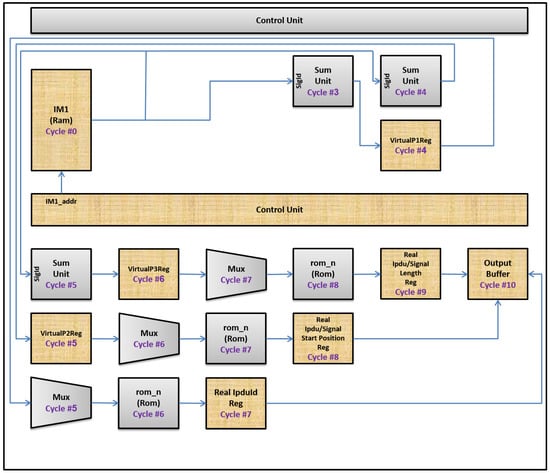
Figure 2.
The additions to AUTOSAR COM ASIP to support the long signal instructions.
In this study, we further extended COM ASIP V2. We introduced six additional instructions, in COM ASIP V3, that perform different hashing operations. These hashing operations secure transmitted PDUs by hashing signals that correspond to these PDUs to ensure the authenticity of such PDUs during transmission. These hashing operations are performed using a two-layer process. This two-layer process modifies the original Galois/counter mode of operation (GCM) algorithm [13,14] to make it faster and increase security of it.
Our paper focuses on two aspects. The first aspect is an automotive cybersecurity feature. This feature involves securing long PDUs in AUTOSAR-based automotive ECUs using a bus-independent HW-based approach. This is done by designing an ISA that contains six hashing instructions that are responsible for ensuring authenticity for such PDUs during transmission and reception to prevent attackers from altering such PDUs. After that, this ISA is realized on an ASIP. The automotive cybersecurity aspect has been addressed by other recent papers [15,16,17] as well, in different ways.
The work in [15,16] aimed to secure communication between ECUs—without the need to authenticate transmitted data—from vulnerabilities of unencrypted communication channels, such as CAN buses. This is done with an intrusion detection system capable of analyzing traffic over the CAN bus and of understanding whether the messages transmitted over the communication channel are malicious or not. This is achieved using a two-step algorithm. The first step is a pre-processing step that is used to filter and verify incoming messages through spatial and temporal analysis to decide whether they may or may not be a possible attack. The second step uses a machine learning technique through a Bayesian network that is trained through a pre-established dataset during the simulation phase. The outcome of the second step is whether we are in the presence or not of an attack.
The second feature of our paper is an optimization aspect, as our paper also focuses on optimizing generic signal-based communication for AUTOSAR-based ECUs. Optimizing performance of AUTOSAR-based ECUs using HW-based approaches is a new field that has been addressed by other papers as well (e.g., optimizing serialization of application data before transmitting them [18]). Our work, in addition to these other ideas, from other papers, can be combined together to provide much greater enhancements for AUTOSAR-based ECUs to cope with the increased speedup of today’s SW applications.
The rest of the paper is organized as follows. Section 2 gives a brief introduction about our previous COM ASIP ISA (i.e., COM ASIP ISA V2). After that, it describes details of a highly secure hashing algorithm, named GCM [13,14]. This algorithm is used by COM ASIP V3. After that, it describes details of a new concept, named two-layer security, that is used by our ASIP to increase the security of the original GCM [13,14]. After that, it describes the changes needed in our ASIP components to support the hashing instructions. After that, it describes the additions that we made in the ISA of our ASIP to support these hashing instructions. Section 3 shows the experimental results. Finally, conclusions are presented in Section 4.
2. Materials and Methods
This section is organized as follows. Section 2.1 gives a brief introduction to our previous COM ASIP ISA (i.e., COM ASIP ISA V2). Section 2.2 describes the details of a highly secure hashing algorithm, named GCM [13,14]. This algorithm is used by COM ASIP V3. Section 2.3 describes details of a new concept, named two-layer security, that is used by our ASIP to increase the security of the original GCM [13,14]. Section 2.4 describes the changes needed in our ASIP components to support the hashing instructions. Section 2.5 describes the additions that we made in the ISA of our ASIP to support these hashing instructions.
2.1. A Brief Introduction to COM ASIP ISA V2
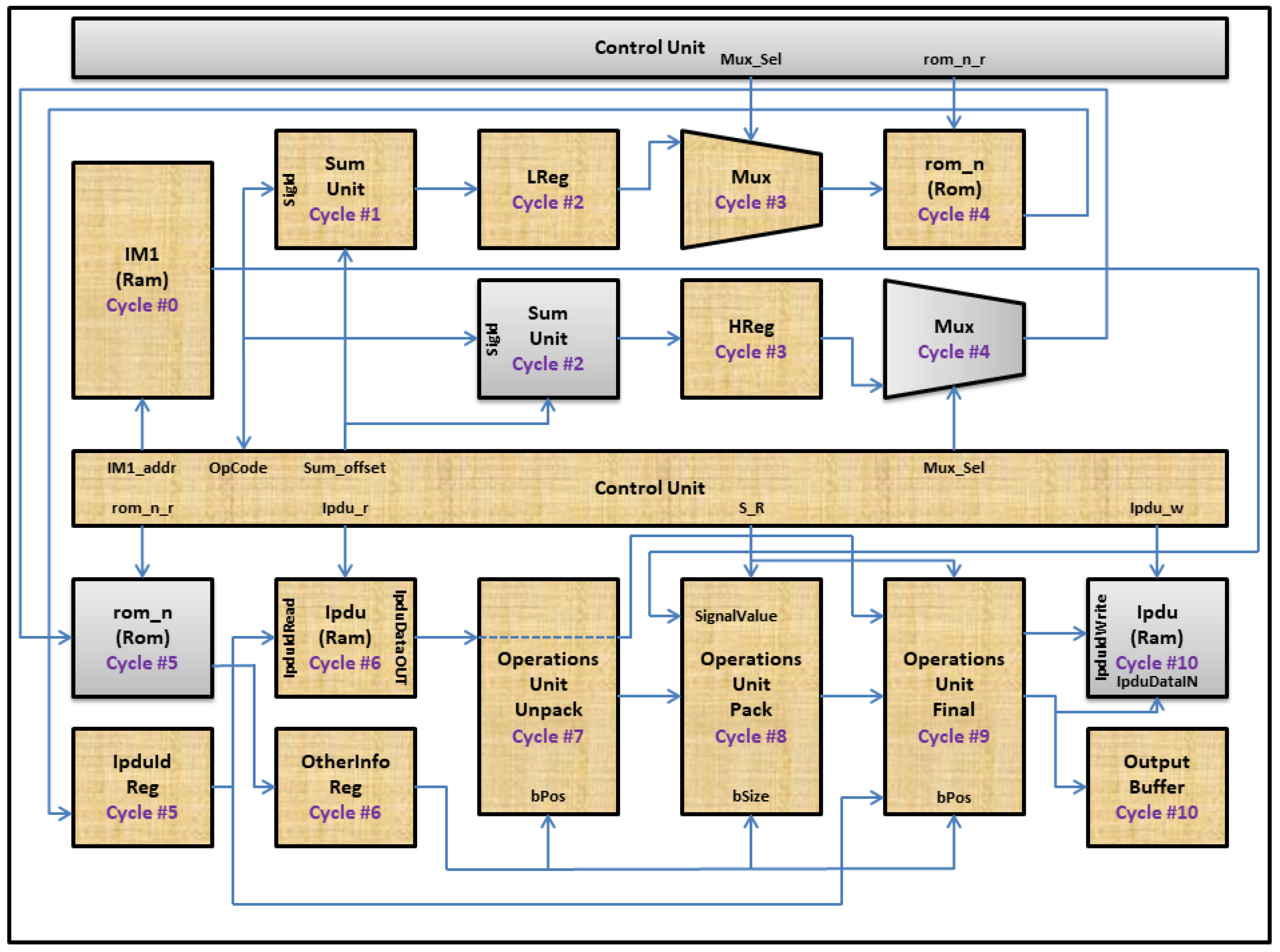
Our previous ISA consists of four phases. These phases are fetching, decoding, execution, and delivery. The execution phase consists of two sub phases (i.e., extraction and packing/unpacking). Our previous ISA supports four instructions (i.e., send signal, receive signal, send long signal, and receive long signal). Each instruction requires 12 cycles (i.e., cycle 0 to cycle 11) to complete its execution.
2.1.1. Actions in Cycle 0
The instruction memory component, named IM1, is activated by the control unit component to fetch a new instruction. The address of this instruction is specified by the IM1_addr control signal.
2.1.2. Actions in Cycle 1
The control unit component decodes an instruction fetched in the previous cycle (i.e., cycle 0) to get three pieces of information, as shown in Figure 3. The first piece, named OpCode, is an instruction type that defines whether this instruction is a send signal, a receive signal, a send long signal, or a receive long signal instruction. The second piece, named SigId/Virtual Signal Id, is an identifier for a virtual signal that is currently processed by this instruction. The third piece, named SigValue/Virtual Signal Value, is a new value for a virtual signal that is currently processed by this instruction.

Figure 3.
Proposed instruction format in the ISA of COM ASIP V2.
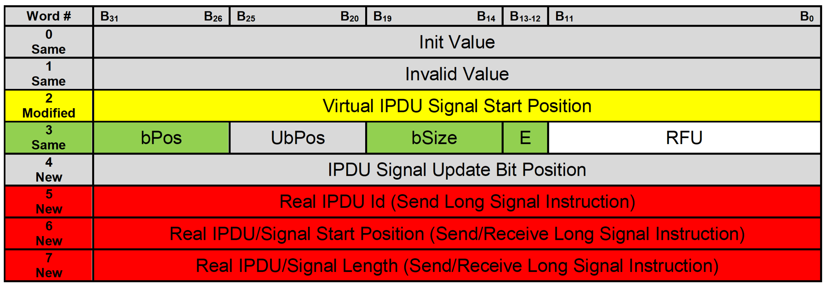
For each virtual signal, there are eight words related to this virtual signal that are saved in a read only memory (ROM) component, named rom_n. These words contain properties that represent which PDUs contain these virtual signals and how these virtual signals are placed inside their corresponding PDUs. The structure of the rom_n component is shown in Figure 4.
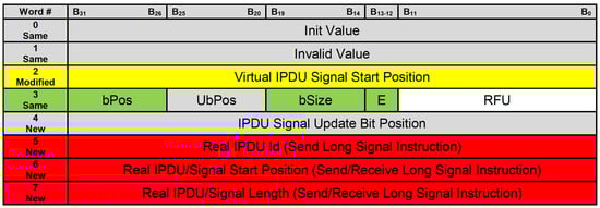
Figure 4.
Encoding of properties for virtual signals inside the rom_n component.
Send Signal and Receive Signal Instructions
We are interested in two words, which are the third and the fourth words. The third word contains the virtual IPDU signal start position that represents the start position of an 8-byte window inside the PDU. This 8-byte window contains a currently processed virtual signal. The fourth word contains four properties that represent how a virtual signal is placed inside its corresponding 8-byte window inside the PDU. These properties are bPos (corresponds to ComBitPosition in the context of AUTOSAR Com [8]), UbPos (corresponds to ComUpdateBitPosition in the context of AUTOSAR Com [8]), bSize (corresponds to ComBitSize in the context of AUTOSAR Com [8]), and E (i.e., Endianness).
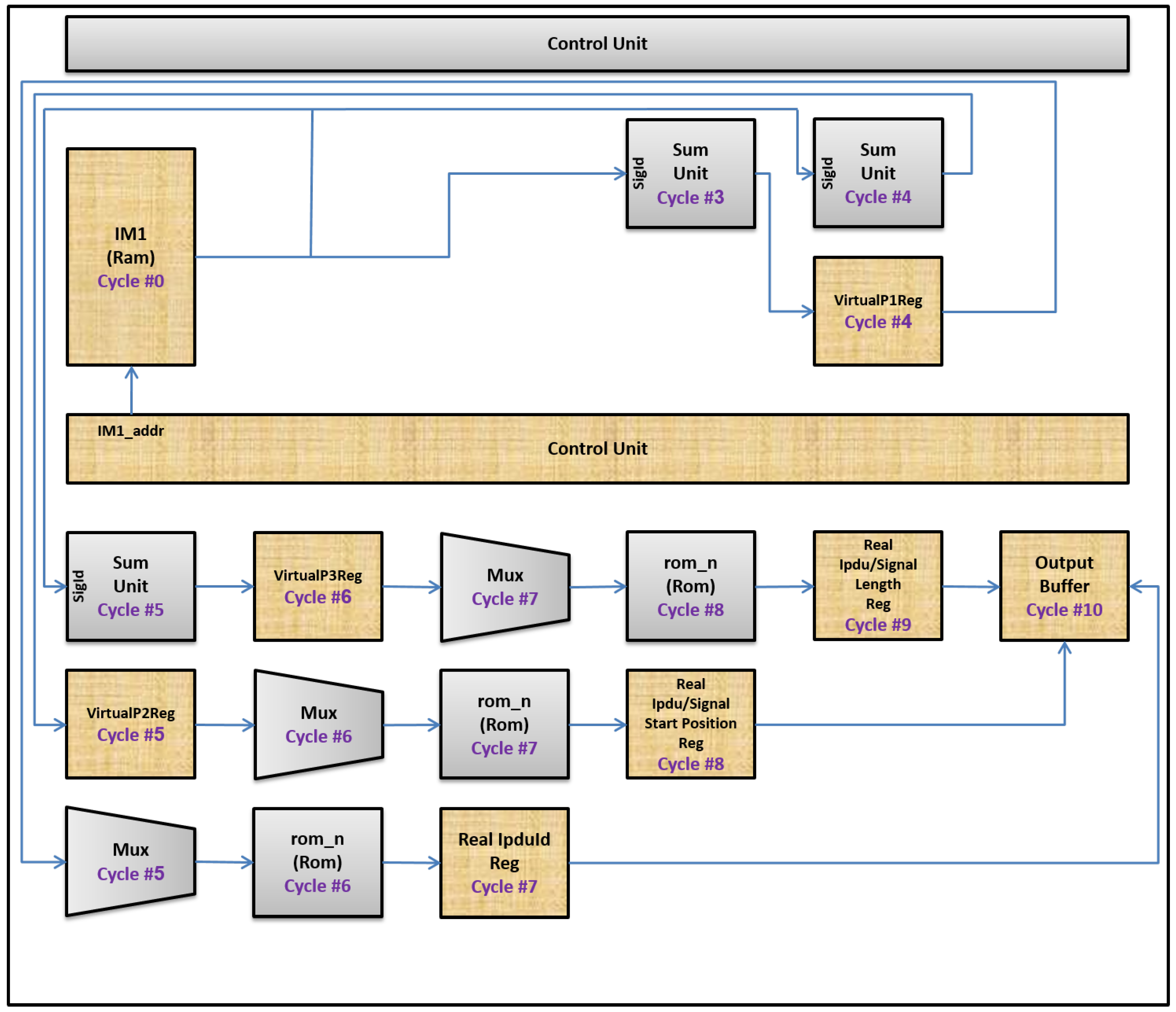
Send Long Signal and Receive Long Signal Instructions
We are interested in three additional words, which are the sixth, seventh, and eighth words. The sixth word contains the real IPDU Id, which represents an identifier for a PDU that contains a currently processed virtual signal and its corresponding real signal as well. The seventh word contains either real IPDU start position or real signal start position. Real IPDU start position will be used in a send long signal instruction to give a position, inside the IPDU component, to lower SW layers to access PDUs after adding (i.e., packing) new values for virtual signals to them. Real signal start position will be used in a receive long signal instruction to give the application layer a position, inside the IPDU component, to access real signals that correspond to virtual signals that are being processed by currently executed instructions. The eighth word contains either real IPDU length or real signal length. Real IPDU length will be used in a send long signal instruction along with real IPDU start position to transfer data, as some of PDUs transmitted from the IPDU component to lower SW layers. Real signal length along with real signal start position will be used in a receive long signal instruction to transfer data from the IPDU component to the application layer.
In cycle 1, the control unit component multiplies SigId by 8 and adds a constant value (i.e., 2) to it to get address of the third word related to this virtual signal in the rom_n component.
2.1.3. Actions in Cycle 2
The control unit component multiplies SigId by 8 and adds a constant value (i.e., 3) to it to get address of the fourth word related to this virtual signal in the rom_n component.
In addition, the control unit component saves the processed SigId (i.e., (SigId * 8) + 2) from the previous cycle (i.e., cycle 1) in the low address register component, named LReg.
2.1.4. Actions in Cycle 3
The control unit component saves the processed SigId (i.e., (SigId * 8) + 3) from the previous cycle (i.e., cycle 2) in the high address register component named HReg.
The control unit component also activates a multiplexer, named Mux, to make its output come from the LReg component.
Only for Send Long Signal and Receive Long Signal Instructions
The control unit component multiplies SigId by 8 and adds a constant value (i.e., 5) to it to get address of the sixth word that corresponds to this virtual signal in the rom_n component.
2.1.5. Actions in Cycle 4
The control unit component activates the rom_n component to read a word from it. The address of this word comes from the LReg component. Data inside the rom_n component at this address contain a virtual IPDU signal start position for a PDU that corresponds to a currently processed virtual signal.
The control unit component also activates the Mux component to make its output come from the HReg component.
Only for Send Long Signal and Receive Long Signal Instructions
The processed SigId (i.e., (SigId * 8) + 5) from the previous cycle (i.e., cycle 3) is saved in the VirtualP1Reg register. In addition, the control unit component multiplies SigId by 8 and adds a constant value (i.e., 6) to it to get the address of the seventh word that corresponds to this virtual signal in the rom_n component.
2.1.6. Actions in Cycle 5
The virtual IPDU signal start position is saved in the IPDU Id Reg component.
The control unit component also activates the rom_n component to read another word from it. The address of this word comes from the HReg component. Data inside the rom_n component at this address contain those four properties that we mentioned above (i.e., bPos, UbPos, bSize, and E). Those properties represent how a virtual signal is placed inside its corresponding 8-byte window inside PDU.
Only for Send Long Signal and Receive Long Signal Instructions
The processed SigId (i.e., (SigId * 8) + 6) from the previous cycle (i.e., cycle 4) is saved in the VirtualP2Reg register. In addition, the control unit component multiplies SigId by 8 and adds a constant value (i.e., 7) to it to get the address of the eighth word that corresponds to this virtual signal in the rom_n component. In addition, the control unit component activates the Mux component to make its output come from the VirtualP1Reg register.
2.1.7. Actions in Cycle 6
The word that is read from the rom_n component in the previous cycle (i.e., cycle 5) is saved in the OtherInfo Reg component.
The control unit component also activates the IPDU component. The IPDU component contains current runtime values for PDUs, to read the current runtime value for an 8-byte window inside the PDU, named the original IPDU value, which corresponds to a currently processed virtual signal. The address used to access the IPDU component comes from the IPDU Id Reg component.
Only for Send Long Signal and Receive Long Signal Instructions
The processed SigId (i.e., (SigId * 8) + 7) from the previous cycle (i.e., cycle 5) is saved in the VirtualP3Reg register. In addition, the control unit component activates the Mux component to make its output come from the VirtualP3Reg register. It also reads a word from the rom_n component; the address of this word comes from the VirtualP1Reg register. This word represents Real IPDU Id. It will be saved in the real IPDU Id Reg component in the next cycle (i.e., cycle 7).
2.1.8. Actions in Cycle 7
The operations unit unpack component uses two inputs, which are bPos, of a currently processed virtual signal, and the original IPDU value. These inputs are used to extract a 32-bit shadow, named original shadow. In case of a send signal/send long signal instruction, this original shadow will be used to place a new value for this currently processed virtual signal in its corresponding 8-byte window inside PDU. In case of a receive signal/ receive long signal instruction, this original shadow will be used to extract current runtime value for this currently processed virtual signal from its corresponding 8-byte window inside PDU.
Only for Send Long Signal and Receive Long Signal Instructions
The control unit component activates the Mux component to make its output come from the VirtualP3Reg register. It also reads a word from the rom_n component, and address of this word comes from the VirtualP2Reg register. This word represents either the real IPDU start position, in case of a send long signal instruction, or real signal start position, in the case of a receive long signal instruction. This word will be saved in the real IPDU/signal start position Reg component in the next cycle (i.e., cycle 8).
2.1.9. Actions in Cycle 8
The operations unit pack component uses three inputs, which are bSize, of a currently processed virtual signal, original shadow, and SigValue. In case of a send signal/send long signal instruction, the operations unit pack component places SigValue—the SigValue extracted in cycle 1—in original shadow based on bSize to construct modified shadow A. In case of a receive signal/receive long signal instruction, the operations unit pack component constructs, based on bSize, modified shadow B that represents the current runtime value for this currently processed virtual signal.
Only for Send Long Signal and Receive Long Signal Instructions
The control unit component reads a word from the rom_n component, and address of this word comes from the VirtualP3Reg register. This word represents either real IPDU length, in case of a send long signal instruction, or real signal length, in case of a receive long signal instruction. This word will be saved in the real IPDU/signal length Reg component in the next cycle (i.e., cycle 9).
2.1.10. Actions in Cycle 9
The operations unit final component uses four inputs, which are modified shadow (i.e., modified shadow A in cases of send signal/send long signal instructions, and modified shadow B in cases of receive signal/receive long signal instructions), bPos, IPDU Id, and original IPDU value. In case of a send signal/send long signal instruction, modified shadow A is added, based on bPos, to the original IPDU value to construct a new value (i.e., final IPDU value). This final IPDU value represents the final value, after adding a new value for this currently processed virtual signal, for the 8-byte window inside PDU that corresponds to this currently processed virtual signal. In case of a receive signal/receive long signal instruction, modified shadow B is passed to the next cycle as it is.
Only for Send Long Signal and Receive Long Signal Instructions
The word read from the rom_n component will be saved in the real IPDU/signal length Reg component, as mentioned above.
2.1.11. Actions in Cycle 10
The output from the previous cycle (i.e., final IPDU value for a send signal/send long signal instruction and modified shadow B for a receive signal/receive long signal instruction) is passed to the output buffer component to be saved. In addition, the final IPDU value for a send signal/send long signal instruction is passed to the IPDU component to save a new value for an 8-byte window inside PDU that corresponds to a currently processed virtual signal.
Only for Send Long Signal and Receive Long Signal Instructions
The output buffer component is activated to save outputs from the real IPDU Id Reg, the real IPDU/signal start position Reg, and the real IPDU/signal length Reg components.
2.1.12. Actions in Cycle 11
In cycle 11, a SW part of Com module can access the output buffer component. In case of a send signal/send long signal instruction, this SW part of the Com module can get, through the output buffer component, a final value for a PDU that corresponds to a currently processed virtual signal. In case of a receive signal/receive long signal instruction, this SW part can get, through the output buffer component, a current runtime value for a currently processed virtual signal from its corresponding PDU.
2.2. The GCM Hashing Algorithm
GCM [13] is a highly secure algorithm that was published by the National Institute of Standards and Technology (NIST) in 2007 [14]. It is currently implemented in many hardware security modules (HSMs) that are parts of many automotive micro-controller units (MCUs). Many papers have optimized implementations of GCM, increasing its throughput and the speed of its internal operations in application-specific integrated circuit (ASIC)-based architectures [19,20,21,22,23] or field programmable gate array (FPGA)-based architectures [24,25,26,27,28,29,30,31]. GCM is also used in network-based systems to secure communication [32,33,34,35,36,37]. GCM has been used in automotive [38] and IOT domains [39,40] as well.
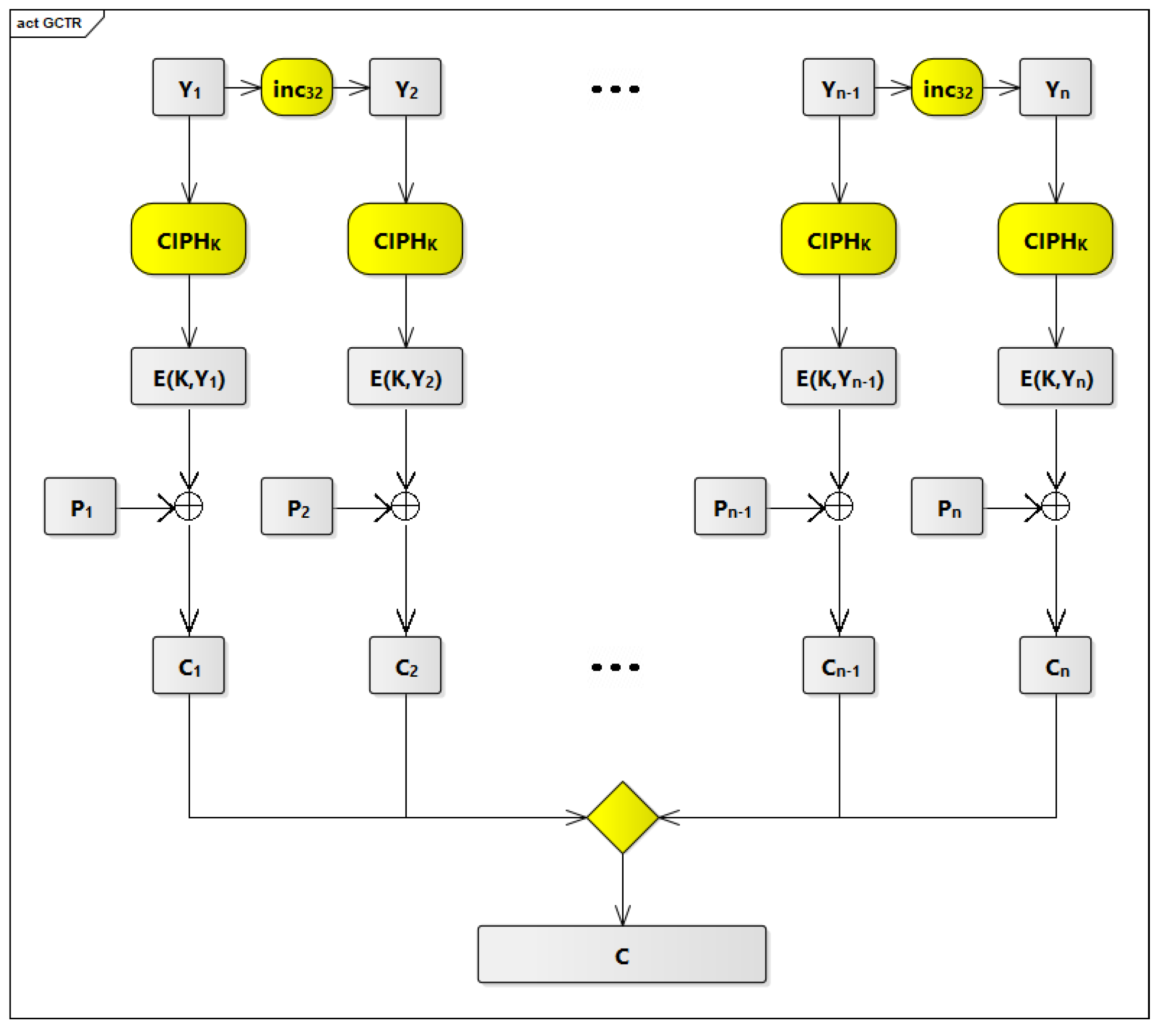
GCM is used for authentication encryption with associated data. GCM provides three main features. The first feature is assurance of confidentiality of input data. This is achieved by encrypting input data using a variation of the counter mode operation of encryption [41], which is a recommended block cipher mode of operation for an Advanced Encryption Standard (AES) [42]. The second feature is assurance of authenticity of confidential data from the previous feature. This is achieved by using a universal hashing function that is defined over a binary Galois (i.e., finite) field. The third feature is assurance of authenticity of additional data that are not encrypted. The GCM authentication encryption process is shown in Figure 5 and Figure 6. The symbols and processes shown in these figures are described in Table 1.
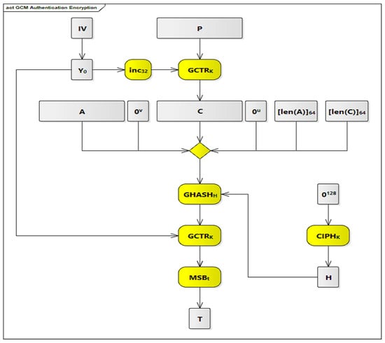
Figure 5.
GCM authentication encryption.

Figure 6.
The GCTR process.

Table 1.
The symbols and processes used in the GCM authentication encryption.
In Figure 5, there are 7 processes that are highlighted in yellow. The first process is the inc function that is used to increment the pre-counter block (Y) each time to generate a new counter block to be used with the GCTR function.
The second process is the GCTR function near the top of the table. This process receives two inputs and produces one output. The two inputs are the plaintext P blocks and the counter blocks. The outputs are the ciphertext C blocks.
The third process is the CIPH function that is used to generate the hash subkey (H) from the zero block (0).
The fourth process is the yellow diamond in the middle of the table. This diamond is an aggregation function that aggregates six inputs. These inputs are the Additional Authenticated Data A; 0, which are 0 bits in length and appended to A; the ciphertext C blocks; 0, which are 0 bits in length u appended to C; [len(A)], which represents the length of A in bits; and [len(C)], which represents the length of C in bits.
The fifth process is the GHASH function that performs a multiplication operation between two inputs and produces one output. The first input is the aggregated data resulting from the fourth process (A 0 C 0 [len(A)] [len(C)]), and the second input is the hash subkey (H) resulting from the third process. The output from the fifth process is one of the inputs to the sixth process.
The sixth process is the GCTR function, shown near the bottom of the table. This process receives two inputs and produces one output. The first input is the output from the fifth process and the second input is the pre-counter block (Y). The output from the sixth process is the input to the seventh process.
The seventh process is MSB, which takes the most significant t bits of the provided input to produce the final tag T.
Figure 6 describes, in detail, the second process (i.e., GCTR function on the top of Figure 5). As described before, the GCTR function receives two inputs and produces one output. The two inputs are the plaintext P blocks P to P and the counter blocks Y to Y. The GCTR function applies the forward cipher function (CIPH) to the second input (i.e., the counter blocks Y to Y) to produce the cipher counters E(K,Y) to E(K,Y). After that, the GCTR function does exclusive-OR (XOR) operations between the cipher counters E(K,Y) to E(K,Y) and the plaintext P blocks P to P to produce the ciphertext C blocks C to C.
2.3. The Two-Layer Security Process Using GCM and COM ASIP
We introduced a two-layer process to increase the security of the GCM hashing algorithm. In order to use GCM with our COM ASIP, we analyzed three designs to construct plaintext. The first option is to consider each PDU as the plaintext that is an input to GCM. The second is to consider each signal as the plaintext that is an input to GCM. The third is the two-layer security process that is described in Section 2.3.3 and Section 2.3.4.
2.3.1. The First Design
For the first design, we need to divide each PDU into blocks of fixed length. The length of each block is 128 bits.
The First Difficulty
The first difficulty in this design comes from the fact that instructions supported by our COM ASIP work with signals but not with PDUs. Supporting this new design will require changing structure of our ASIP, introducing many new components and data paths, and changing the ISA of our ASIP completely, which will affect both the flexibility and performance of our ASIP.
The Second Difficulty
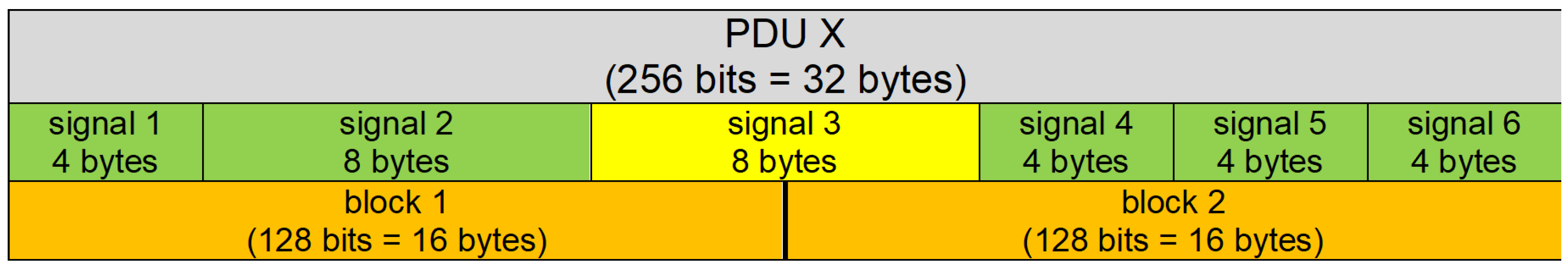
Another difficulty comes from the fact that signals differ from each other in their sizes and positions within PDUs. By dividing PDUs into 128-bit blocks, we might find that one signal, based on the position and size of this signal within its corresponding PDU, spans over two consecutive blocks, as shown in Figure 7, where signal 3 spans over block 0 and block 1. This will also complicate our ASIP and affect its flexibility and performance. Based on the previous points, we discarded that design choice.
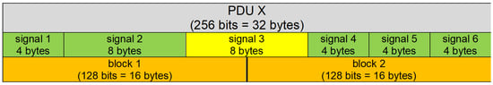
Figure 7.
Signal spans over two consecutive blocks.
2.3.2. The Second Design
For the second design, we need to divide each signal into blocks of fixed length, where length of each block is 128 bits. A signal can fit into one block if its length is ≤128 bits. If the length of the signal is >128 bits, it is divided into more than one block. In both cases, padding is used, if it is necessary, to have complete blocks (i.e., length of input data is multiple of block length).
A Better Design
This design is better than the first design. The reason is that instructions supported by our COM ASIP already work with signals, so we do not need to introduce many changes in the structure of our ASIP. Although this design seems better than the first design, it has two main difficulties.
The First Difficulty
The first difficulty is that this design requires reserved bytes for each signal to contain its hash value, which will require transmitting much more data from sender ECUs to deliver hashes of such signals to receiver ECUs so receiver ECUs can verify such signals correctly. This will consume the bandwidth of communication buses that connect ECUs and will decrease the throughput of such communication buses to transmit actual data. Table 2 shows the utilization percentage, to transmit actual data, of communication buses when we use different tag lengths. The original tag length is 128 bits, and truncated tag lengths can be smaller (16 bits, 32 bits, 64 bits, etc.). The red color indicates that the utilization percentage is less than 50%, the green color indicates utilization percentage is more than 50%, and the yellow color indicates utilization percentage is 50%. As we can see, the utilization percentage is less than 50% in most of cases, which impacts the throughput of the communication buses and affects the performance and usability of our design.
Table 2.
Utilization percentages of communication buses using different tag lengths and signal sizes.
The Second Difficulty
The second difficulty is that we need to change the structure of the PDUs to have room to hold hash values for signals contained in these PDUs. We have two approaches. The first approach is to add these hash values to the ends of PDUs. The second approach is to allow each signal to have its own hash directly after its end, which requires shifting positions of the following signals in this PDU and changing the structure of this PDU completely. Both problems, as we can see, affect the performance and flexibility of this design choice, so we discarded this design choice as well.
2.3.3. The Third Design
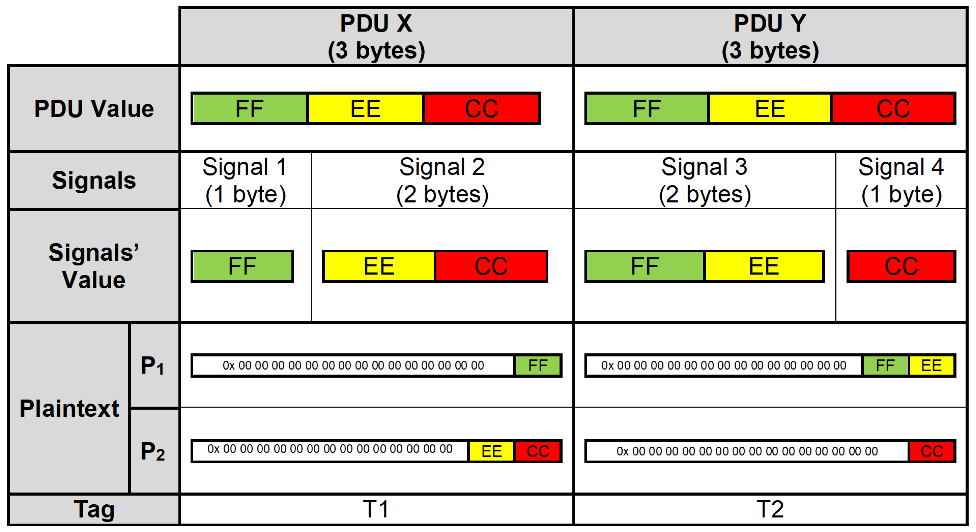
The third designis similar to the first design. We consider each PDU as the plaintext that as an input to the GCM, and there is only one hash value for each PDU. The difference is that we do not divide each PDU into blocks of fixed length. Instead, we consider each virtual signal in these PDUs as one block, and padding is used to complete the block. The next signal in this PDU is considered as the next block in this plaintext, the third signal is considered as the third block in this plaintext, etc.
The First Layer of Security
The first layer of security in this design comes from GCM itself, as any attacker needs to know IV and K to bypass the authenticity of the transmitted data and alter them if needed.
The Second Layer of Security
The second layer of security comes from the fact that even if any attacker breaks the first layer of security by knowing IV and K, he will not be able to use them to alter a transmitted PDU. This is because he also needs to know how signals are placed inside these PDUs, which differs based on positions and sizes of signals inside these PDUs, from one PDU to another.
Two Identical PDUs with Different Tags
Figure 8 shows two PDUs, where data transmitted by these PDUs are identical. Even if data transmitted by these PDUs are identical, tag values T1 and T2 are different, which are tags that are generated for these PDUs by GCM that are appended to these PDUs. The reason comes from the fact that the internal structures of these PDUs are different, as positions and sizes of signals contained in these PDUs are different. This will lead to different values inside blocks that will construct the plaintext. P1 and P2 are plaintext blocks constructed from these PDUs that are inputs to GCM.
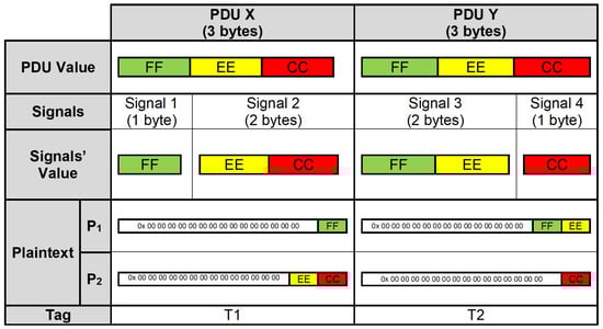
Figure 8.
Two identical PDUs with different tags.
More Security
Based on the previous points, attackers also need to know positions and sizes of all signals inside ECUs to be able to break the second layer of security, which is much more complex than using only one layer of security.
2.3.4. The Modified GCM Algorithm
In order to integrate GCM within our COM ASIP, we have made some modifications to the original GCM to make it faster. The modified GCM algorithm is shown in Figure 9. The modifications that we have been made are based on identifying possible processes, in the original GCM algorithm, which can be done offline.
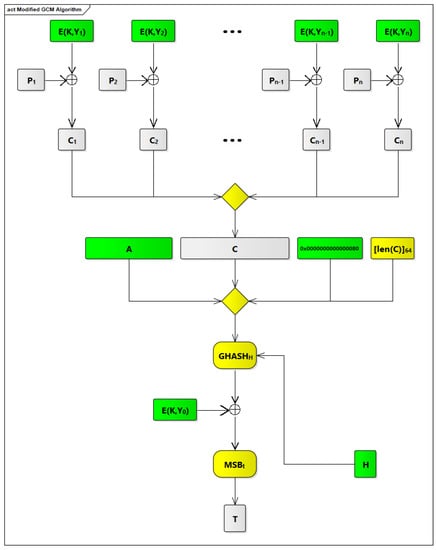
Figure 9.
The modified GCM algorithm.
The First Offline Process (Generating Y from IV)
The first process is generating Y from IV. This process has to be done online in case IV can be changed. In the context of our COM ASIP, IV is static and has a fixed length, 96 bits, so converting IV to Y can be done offline, and Y is saved in a secure memory component that is part of our ASIP.
The Second Offline Process (Generating E(K,Y))
The second process applies CIPH to Y. This process (i.e., E(K,Y)) is part of the GCTR process that is applied to the output from the GHASH process. In the context of our COM ASIP, Y is static because IV is static, so E(K,Y) is static as well and can be done offline. E(K,Y) is saved in a secure memory component that is part of our ASIP. Based on the previous points, the GCTR process that is applied to output from GHASH process will turn out to be an XOR operation between E(K,Y) and output from the GHASH process. This is shown in Figure 9.
The Third Offline Process (Incrementing Y and Generating Y to Y)
The third process is incrementing Y to generate counters, Y to Y, which is used as inputs to the GCTR process that is applied to plaintext blocks. This process can be done offline, and these counters, Y to Y, is saved in a secure memory component that is part of our COM ASIP.
The Fourth Offline Process (Generating E(K,Y) to E(K,Y))
The fourth process is applying CIPH to counters Y to Y. This process (i.e., E(K,Y) to E(K,Y)) is part of the GCTR process that is applied to plaintext blocks. In the context of our COM ASIP, Y to Y are static because Y is static, so E(K,Y) to E(K,Y) are static and can be performed offline. E(K,Y) to E(K,Y) is saved in a secure memory component that is part of our ASIP. Based on the previous points, the GCTR process that is applied to plaintext blocks will involve XOR operations between plaintext blocks (i.e., P to P) and E(K,Y) to E(K,Y). This is shown in Figure 9. To simplify the design of our ASIP and increase its efficiency and operability, counters are limited to 64 counters, from Y to Y, to reduce the size of secure memories that is used to save these counters (i.e., Y to Y) and their corresponding cipher values (i.e., E(K,Y) to E(K,Y)).
The Fifth Offline Process (Calculating the Length of AAD)
The fifth process is calculating the length of AAD. In the context of our COM ASIP, AAD is only one block (i.e., its length is 128 bits), so it has a fixed length, and [len(A)] can be replaced, as shown in Figure 9, by a static value (i.e., 0x0000000000000080).
The Sixth Offline Process (Appending vs. Bits to AAD)
The sixth process is appending vs. bits to AAD. This process (i.e., 0) was eliminated, as the length of AAD is ma ultiple of block length (i.e., length of AAD is 128 bits, which corresponds to one block).
The Seventh Offline Process (Appending u Bits to C)
The seventh process is appending u bits to C. This process (i.e., 0) was eliminated, as the length of C is a multiple of block length. We ensured this because, based on the third design in Section 2.3.3 that we selected, each virtual signal is considered as one plaintext block, and each PDU contains a number of virtual signals, so we have a number of complete blocks that represents this PDU.
The Eighth Offline Process (Generating H)
The eighth process is generating H from the zero block. The zero block (i.e., 0) is static, so H (i.e., E(K,0)) is static as well. Thus, generating H from the zero block can be done offline, and H is saved in a secure memory component that is part of our COM ASIP.
The Modified GCM Algorithm
Based on the previous offline processes, we modified the original GCM algorithm, and our modified design, as shown in Figure 9, is integrated within our COM ASIP. This modification is described in Section 2.4. In Figure 9, the components and processes that are done offline are highlighted in green, and those that are done online are highlighted in yellow.
Secure Memory Components Are Needed
Based on those offline processes, we concluded that we need secure memory components. These memory components are used to save Y, E(K, Y), and Y to Y; and E(K,Y) to E(K,Y) and H. Y and Y to Y can be removed from these secure memory components because they will not be used directly, as shown in Figure 9, in our modified GCM algorithm. The only secure memory components that are needed are those that are used to save E(K, Y) and E(K,Y) to E(K,Y) and H.
2.4. The Changes and Additions in COM ASIP Components to Support the Hashing Instructions
The format of instructions, in the IM1 component, in COM ASIP V3, is kept same as the format of instructions in COM ASIP V2. The only difference is that six new hashing instructions are supported, as shown in Table 3, so our COM ASIP V3 supports 10 instructions. These new hashing instructions work in a similar way to the receive signal and the receive long signal instructions. These hashing instructions will get values for signals specified by these instructions, and then the modified GCM algorithm is used to calculate and update tag values for PDUs, based on values for signals specified by these hashing instructions, which contain these signals.
Table 3.
The instructions supported by different versions of COM ASIP.
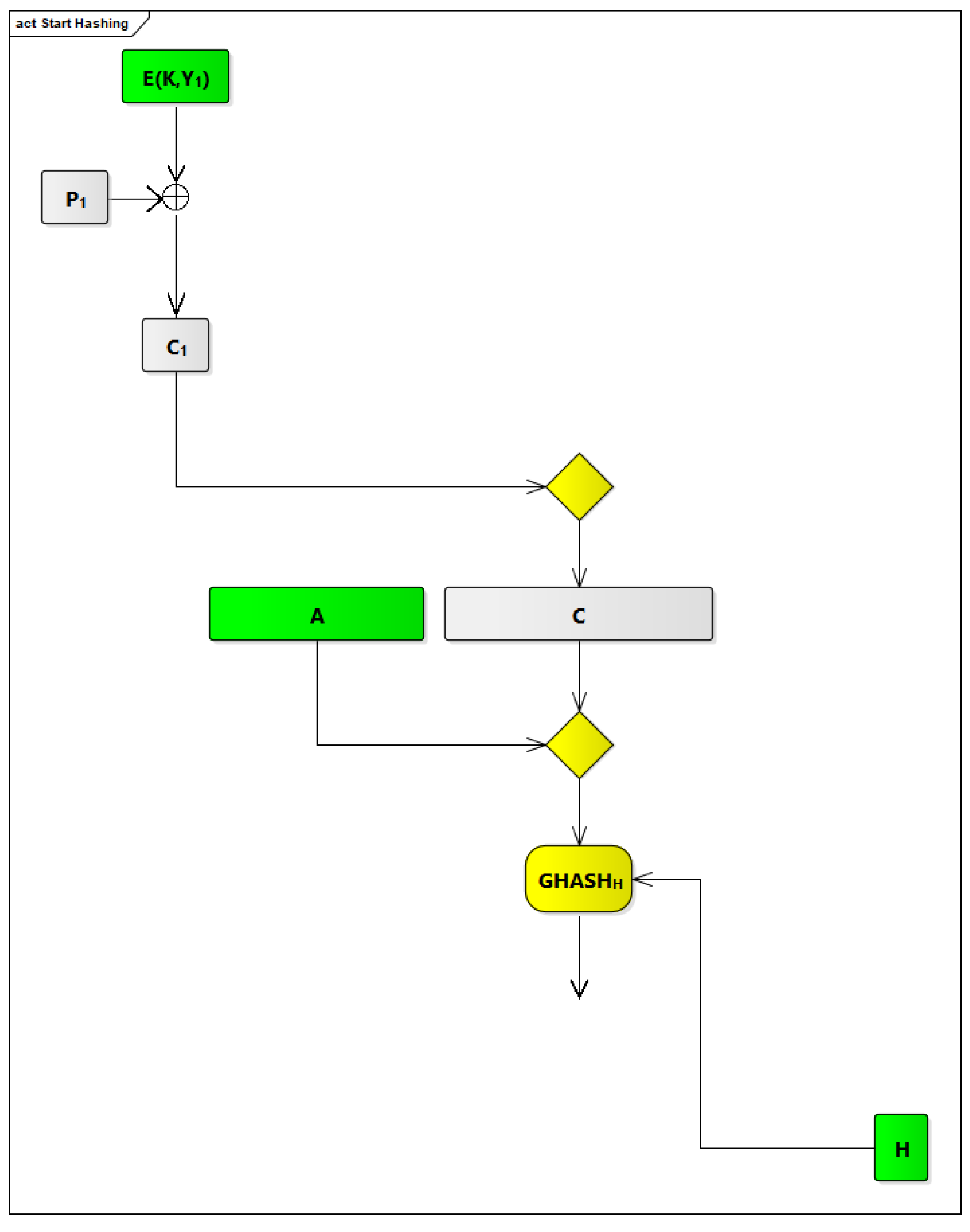
2.4.1. The Start Hashing Instruction
This instruction is used to start the hashing process, using the modified GCM algorithm, for the first signal (i.e., P) in a given PDU to generate the first ciphertext block (i.e., C). It is used as well to prepare AAD and apply the GHASH process to merged input A C. The components and processes from the modified GCM algorithm used by this instruction are shown in Figure 10.

Figure 10.
Start hashing instruction flow.
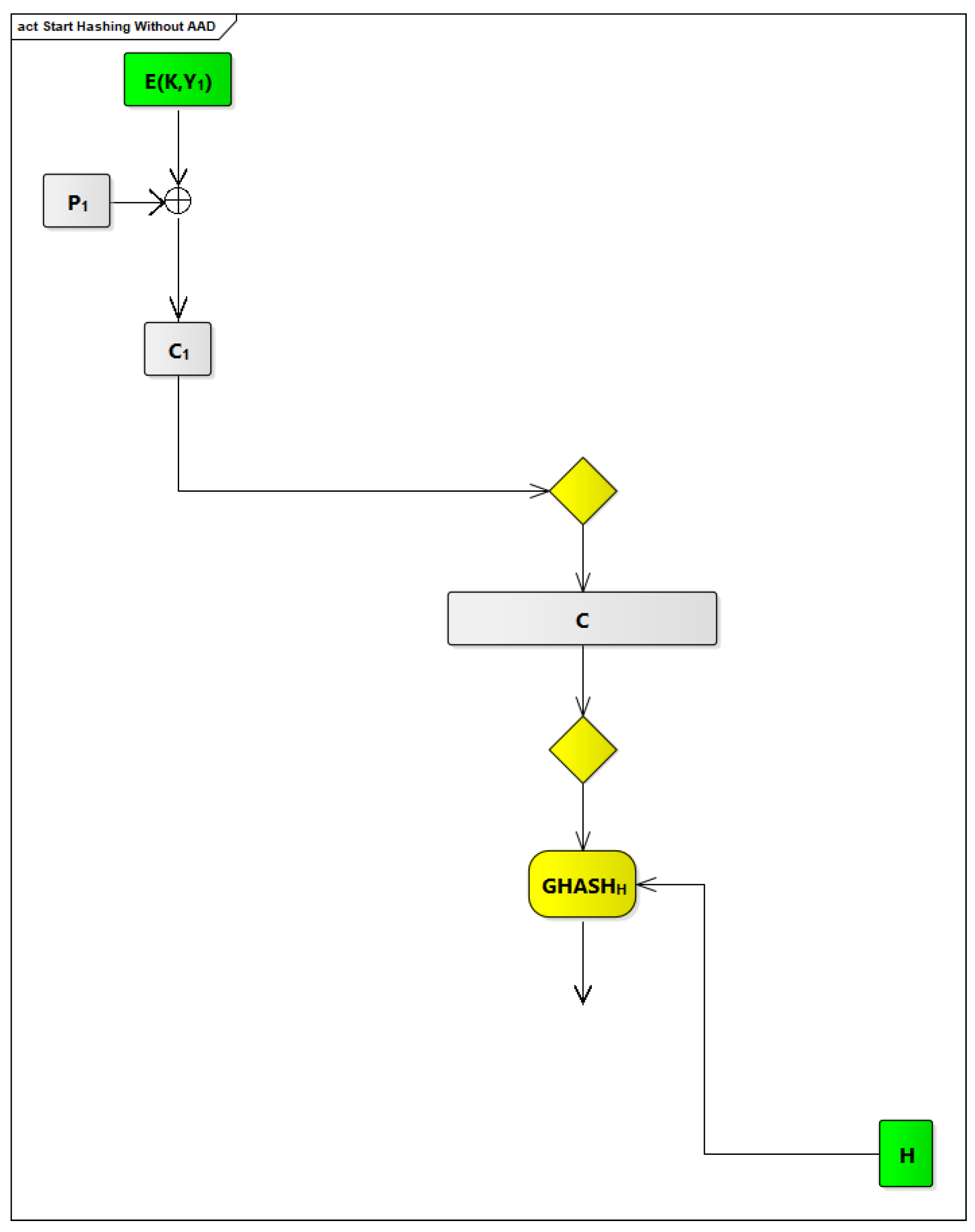
2.4.2. The Start Hashing without AAD Instruction
This instruction is similar to the start hashing instruction. The only differences, as shown in Figure 11, are that no AAD is used and that the GHASH process is applied directly to C.
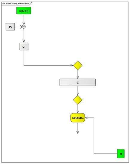
Figure 11.
Start hashing without AAD.
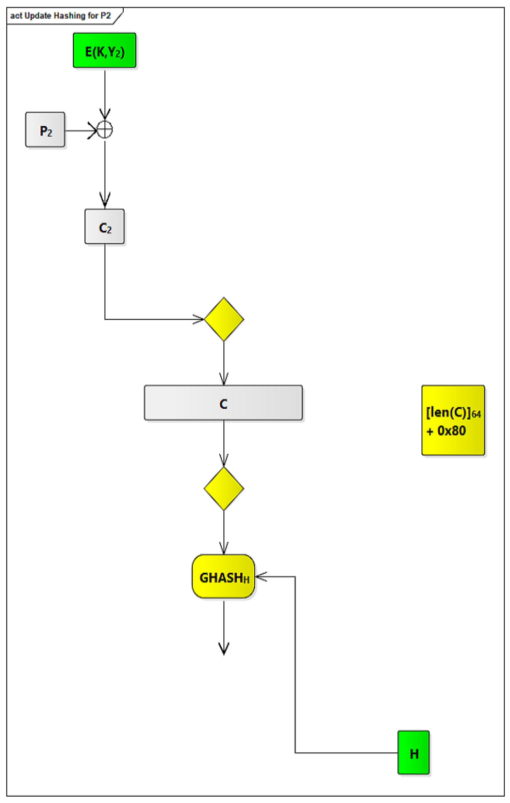
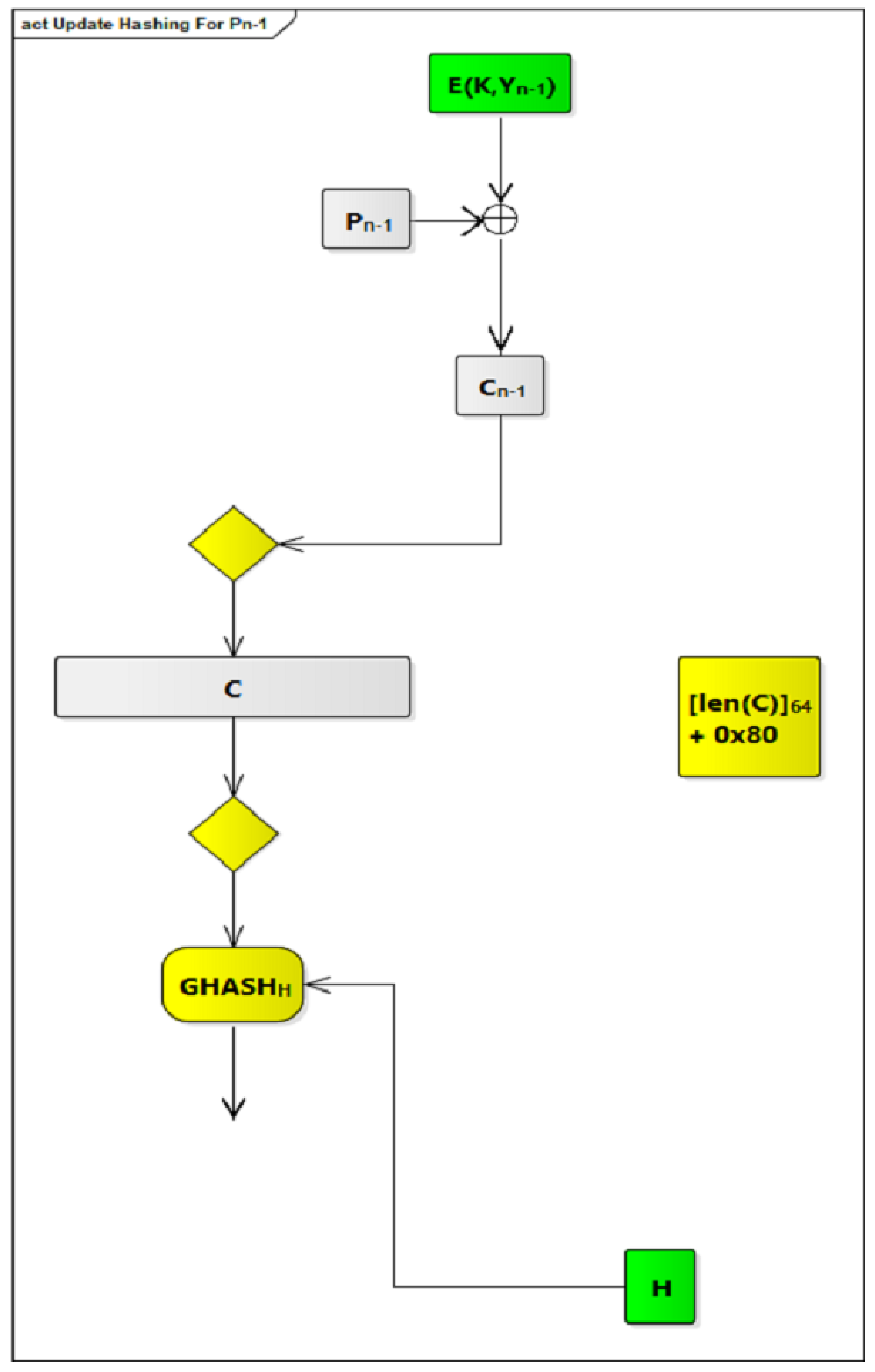
2.4.3. The Update Hashing Instruction
This instruction is used to continue the hashing process, using the modified GCM algorithm, for the next consecutive signals (i.e., P to P) in a given PDU to generate the next consecutive ciphertext blocks (i.e., C to C). It is also used to apply the GHASH process to these ciphertext blocks (i.e., C to C). This instruction increments the length of the ciphertext by 0x80, which is the length of a 128-bit block in bits, per invocation of this instruction. Figure 12 and Figure 13 show how this instruction is performed for P and P consecutively, where each invocation of this instruction is responsible for only one plaintext block.

Figure 12.
Update hashing for P.
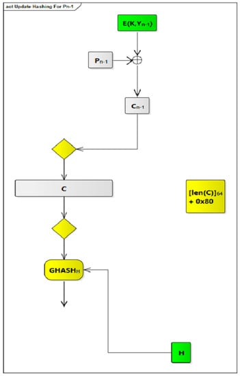
Figure 13.
Update hashing for P.
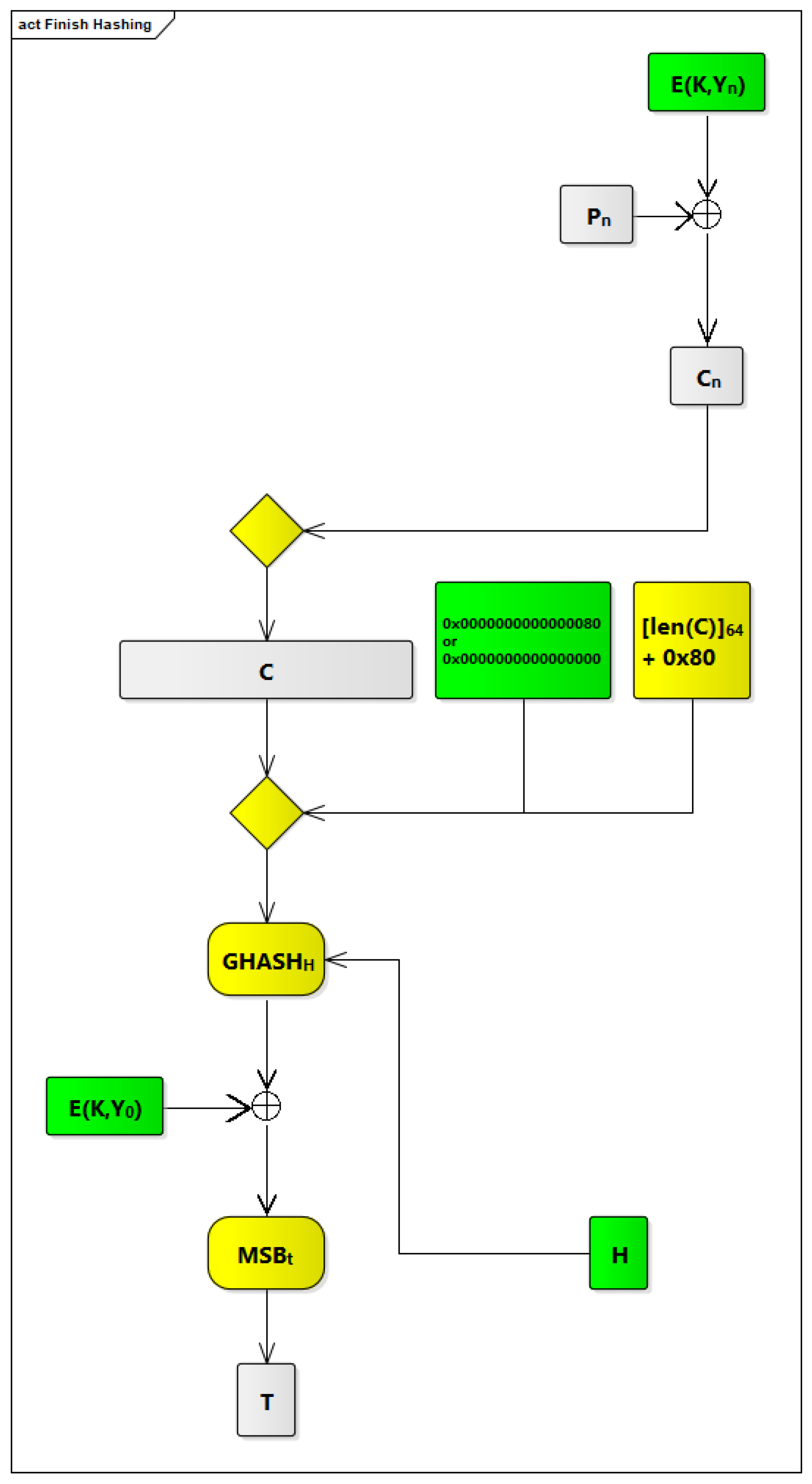
2.4.4. The Finish Hashing Instruction
This instruction is used to finish the hashing process, using the modified GCM algorithm, for the last signal (i.e., P) in a given PDU. It applies the GHASH process to the last ciphertext block (i.e., C). It increments the length of the ciphertext by 0x80 to reflect length of the last ciphertext block. It produces a final value for AAD, where value for AAD is either 0x80 or 0x00. 0x80 is used in cases where the first signal in this PDU is processed using a start hashing instruction. 0x00 is used in cases where the first signal in this PDU is processed using a start hashing without AAD instruction. After that, it applies the GHASH process to the counter block ([len(A)] [len(C)]). After applying GHASH process, an XOR operation is performed between the block generated by the GHASH process and E(K,Y) to generate a tag that should be appended to this PDU upon transmitting it. This tag is used to ensure authenticity of this PDU and make sure it will not be altered by attackers. Figure 14 shows how this instruction is performed.
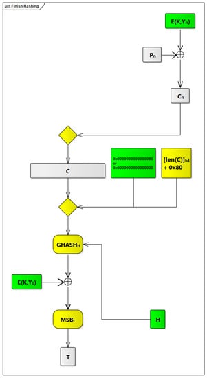
Figure 14.
Finish hashing instruction flow.
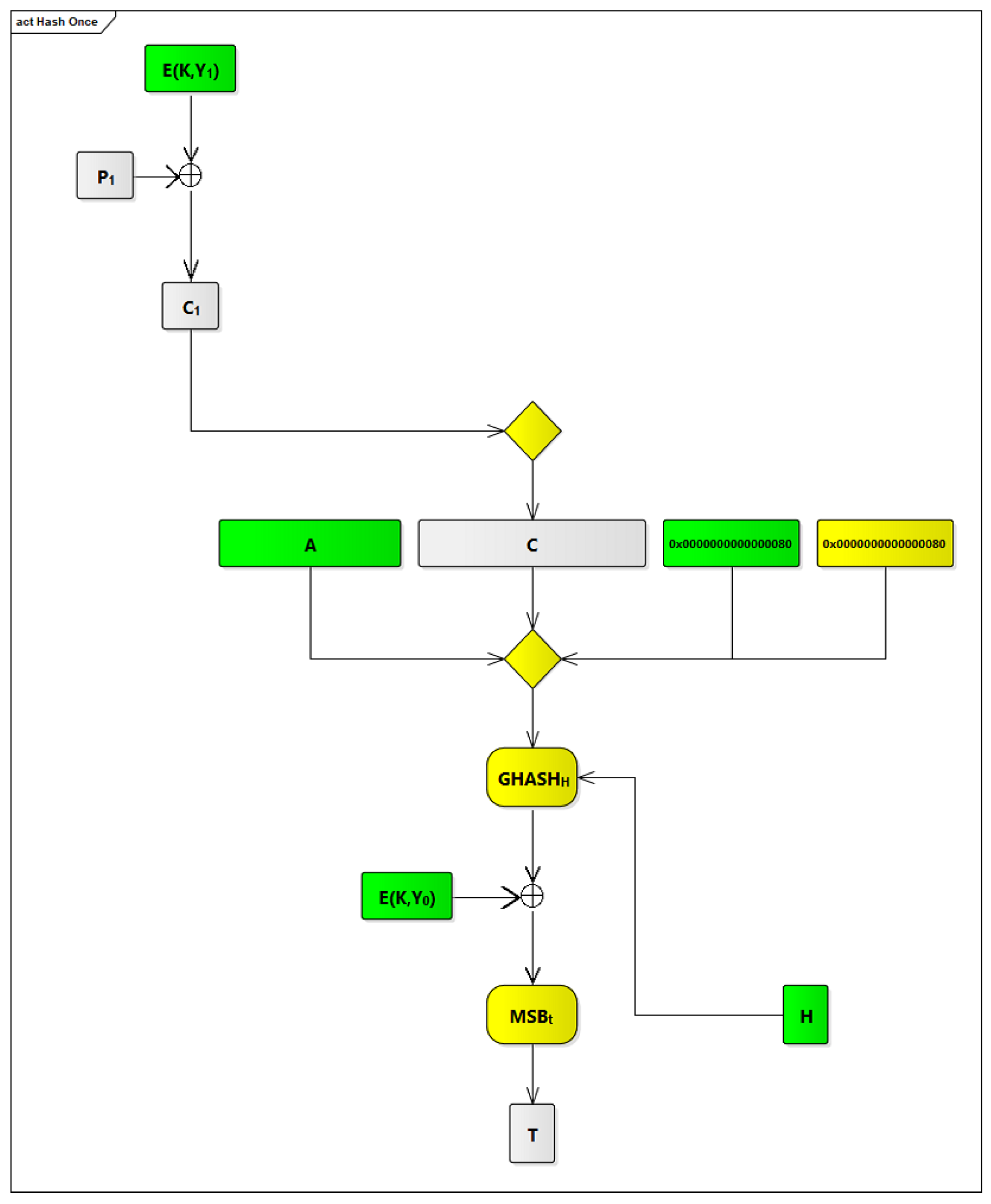
2.4.5. The Hash Once Instruction
This instruction is used if there is only one signal inside a given PDU. This instruction performs the hashing process, using the modified GCM algorithm, for this signal along with AAD and merged input [len(A)] [len(C)]. [len(A)] is 0x80 because there is only one AAD block. [len(C)] is 0x80 because there is only one block in plaintext that is represented by the signal specified by the hash once instruction. Figure 15 shows how this instruction is performed.
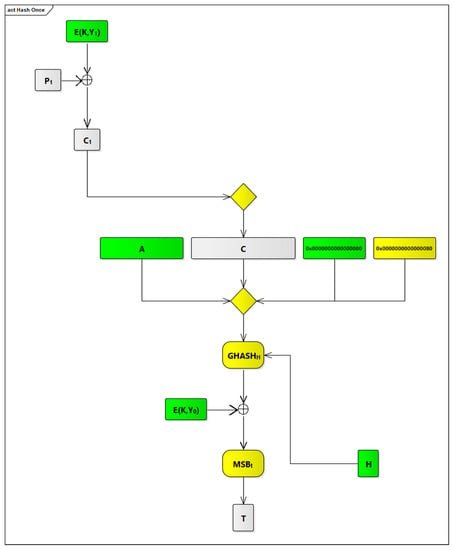
Figure 15.
Hash once instruction flow.
2.4.6. The Hash Once without AAD Instruction
This instruction is similar to the hash once instruction. The only differences, as shown in Figure 16, are that no AAD is used and that [len(A)] is 0x00 in this case.
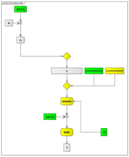
Figure 16.
Hash once without AAD.
2.4.7. The Modified rom_n Component
The structure of the rom_n component is same as the one that we used in COM ASIP V2, as shown in Figure 4, and there is no need to add any extra words to it.
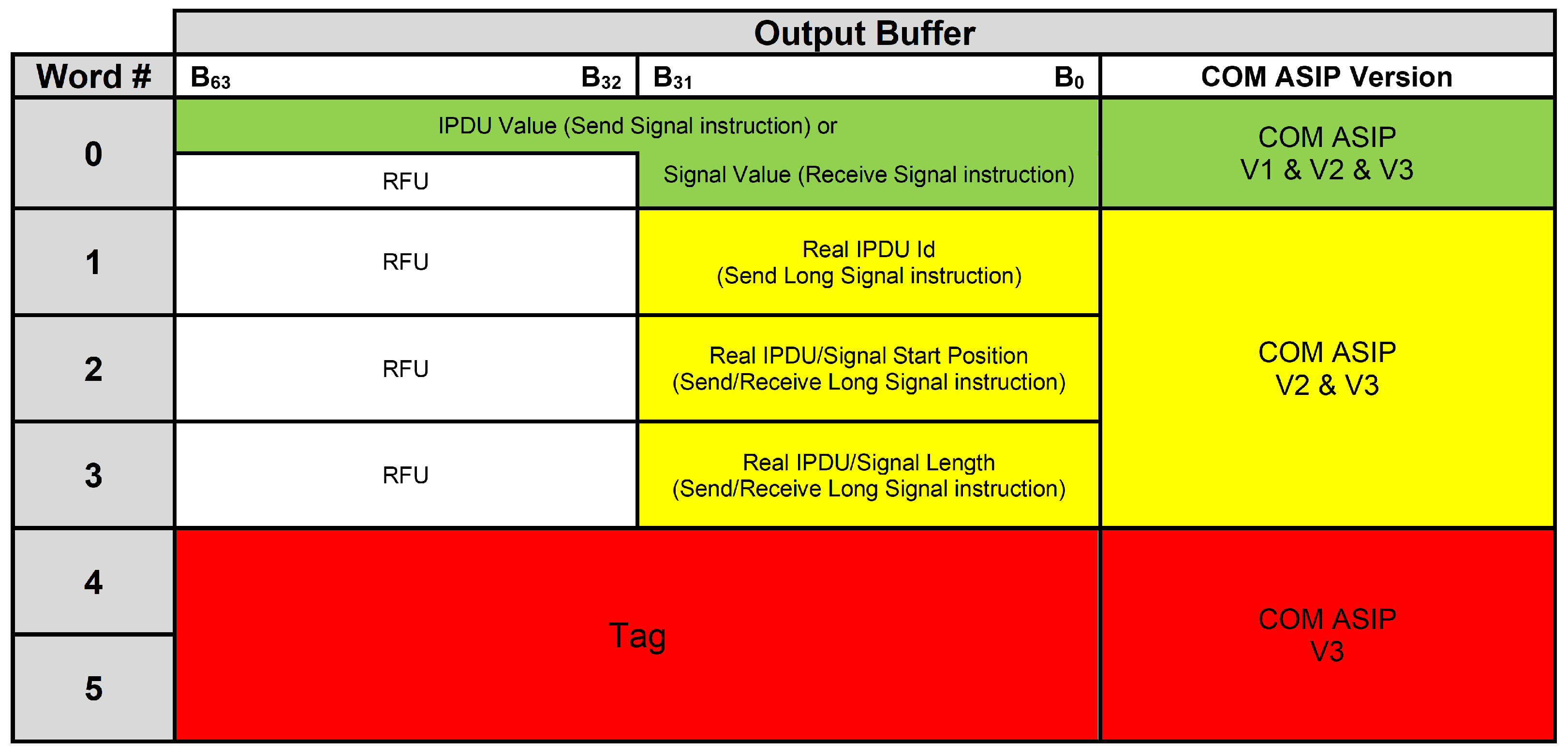
2.4.8. The Modified Output Buffer Component
The output buffer component has been extended, as shown in Figure 17, to contain two extra words that will be reserved for a tag value that should be appended to each PDU upon performing a finish hashing, a hash once, or a hash once without AAD instruction.
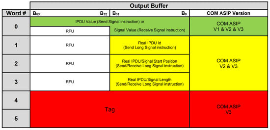
Figure 17.
The modified output buffer component.
2.4.9. Extra ROM Components
As described previously, we need secure memory components to save E(K,Y) and E(K,Y) to E(K,Y) and H. We extended our COM ASIP to contain three additional secure memory components (i.e., they can be only read by our COM ASIP during its internal operation). The first one, named the cipher pre-counter register, is a 128-bit register that will be used to save E(K,Y). The second one, named cipher counters memory, is a group of 64 registers, where width of each register is 128 bits. The cipher counters memory will be used to save E(K,Y) to E(K,Y). The third one, named the cipher zero vector register, is a 128-bit register. The cipher zero vector register contains H that is equivalent to E(K,0). We added an additional fourth memory component, named the AAD register, that is used to save AAD. The AAD register is a 128-bit register because the length of AAD in our current COM ASIP design is restricted to one block (i.e., 128 bits). It is not mandatory to make this fourth component secure. These components are shown in Figure 18.
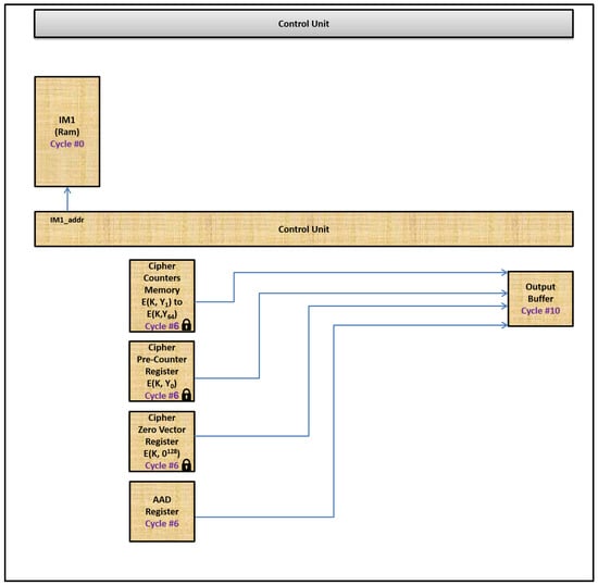
Figure 18.
The additions to AUTOSAR COM ASIP to support the hashing instructions.
2.5. The Additions to COM ASIP ISA to Support the Hashing Instructions
The additions to COM ASIP V2 to support the hashing instructions are shown in Figure 18. For the previous send long signal and receive long signal instructions, no changes in instruction flow during the twelve execution cycles are needed. These instructions (i.e., the send long signal and the receive long signal instructions) work without any extra logic to handle them in COM ASIP V3. For the hashing instructions, the changes in instruction flow are illustrated below.
2.5.1. Changes in Cycles 0, 1, 2, 3, 4, and 5
In cycles 0, 1, 2, 3, 4, and 5, no changes are expected.
2.5.2. Changes in Cycle 6
In cycle 6, the control unit component checks which hashing instruction is currently being executed. It activates, based on the hashing instruction, the needed memory components to read a word from each of them. Table 4 shows which memory components that will be activated.
Table 4.
The actions performed by the control unit component to support the hashing instructions.
2.5.3. Changes in Cycle 7, 8, and 9
In cycle 7, 8, and 9, no changes are expected.
2.5.4. Changes in Cycle 10
In cycle 10, the output buffer component is activated to apply the GHASH process, using the inputs received from cycle 6, to update a tag value that should be appended to a given PDU. Upon executing a finish hashing, hash once, or hash once without AAD instruction, a final tag value for a PDU that is currently processed is placed in the output buffer component.
2.5.5. Changes in Cycle 11
In cycle 11, no changes are expected.
3. Experimental Results
This section is divided into two sections. Section 3.1 contains synthesis results of our new COM ASIP (i.e., COM ASIP V3) and a comparison between them and those of our previous COM ASIP (i.e., COM ASIP V2). Section 3.2 lists results of a throughput comparison between our new COM ASIP and different communication buses.
3.1. Synthesis Results of COM ASIP V3
Our new COM ASIP (i.e., COM ASIP V3) has been synthesized on Artix-7 FPGA. The target device used for synthesizing COM ASIP V3 was an xc7a100t-3-csg324. Logic utilization from synthesizing COM ASIP V3 is shown in Table 5. These synthesis results were generated by synthesizing a COM ASIP instance working on 2000 virtual signals. Each signal needs 8 bytes in the rom_n component to save its related information, so the rom_n component has a size of 16 kB, whereas the IPDU component has a size of 1.6 kB. The size of the IPDU component depends on the number of PDUs contained in COM ASIP and the lengths of these PDUs. Each PDU contains one or more signals out of these 2000 virtual signals mentioned before. Each signal has a different length. The maximum length of each signal is 32 bits.
Table 5.
Logic utilization from synthesis results for COM ASIP V3.
The above number of signals and their lengths were selected for compatibility with our previous COM ASIP (i.e., COM ASIP V2). We used 2000 virtual signals [12]. Sizes of the IPDU component and the rom_n component for our previous COM ASIP were the same as the sizes of the IPDU component and the rom_n component in our new COM ASIP (i.e., COM ASIP V3). A comparison between the logic utilization of our previous COM ASIP and COM ASIP V3 is shown in Table 6. The Diff. column represents an increase in logic utilization by COM ASIP V3 compared to COM ASIP V2, with respect to FPGA resources.
Table 6.
Comparison between logic utilization of COM ASIP V2 and COM ASIP V3.
The experimental results show that there is an increase in logic utilization in COM ASIP V3 compared to COM ASIP V2. The highest percentage of increase, as shown in Table 6, is in slice LUTs. This is due to adding GHASH function in the output buffer component. This function performs multiplication operations for the binary Galois (i.e., finite) field of 2 elements, so it requires many slice LUTs to perform these operations. There is an increase in block RAM/FIFO, as shown in Table 6. This increase is due to adding secure memory components to save E(K, Y) and E(K,Y) to E(K,Y) and H.
There is an increase in the minimum clock period. This is because of the GHASH function that is part of the critical path, because of its multiplication operations, in the ISA of COM ASIP V3. However, this increase is not significant (i.e., +31.7%). This means that COM ASIP V3 can still handle (i.e., send and receive) long signals and secure PDUs with the same performance.
We performed the same tests (i.e., transmitting/receiving a 64-byte CAN FD frame and a 254-byte FlexRay frame) [12] using COM ASIP V3. COM ASIP V3 was able to handle a 64-byte CAN FD frame in . It was able to handle a 254-byte FlexRay frame in . These measurements can be verified using the same approach that has been used with COM ASIP V2. The only changes were using the maximum clock frequency and the minimum clock period, as shown in Table 5, for COM ASIP V3 calculations.
3.2. Throughput Comparison between Our New COM ASIP and Different Communication Buses
The throughput achieved by our new COM ASIP (i.e., COM ASIP V3) has been compared, as shown in Table 7, against the throughput of CAN FD and FlexRay communication buses. The throughput achieved by our new COM ASIP is much more, 42× to 75×, than the throughput needed by these high-speed communication buses.
Table 7.
Throughput comparison between COM ASIP V3 and different communication buses.
For example, transmitting a 64-byte CAN FD frame on CAN bus running on 1 Mbit/s baud rate (i.e., the highest baud rate for CAN bus) takes 118 [12], and transmitting a 254-byte FlexRay frame on FlexRay bus running on 10 Mbit/s baud rate (i.e., the highest baud rate for FlexRay bus) takes [12]. However, COM ASIP V3 can handle (i.e., transmit, receive, calculate hash, or hash verify) a 64-byte CAN FD frame and a 254-byte FlexRay frame in or , respectively.
4. Conclusions
Our paper introduced a bus-independent HW-based approach to secure long PDUs in AUTOSAR-based automotive ECUs by designing an ISA and realizing it on an ASIP. This approach is a new approach that has not been reported before for AUTOSAR-based ECUs.
We extended the ISA of our previous ASIP by introducing six new instructions to COM ASIP V3, to hash PDUs that contain long signals to authenticate transmission and reception of such PDUs. Our new ISA, similarly to the previous ISA, consists of four phases. These phases are fetching, decoding, execution, and delivery. With this new extension, our new ISA can secure these PDUs by hashing signals that correspond to these PDUs to ensure the authenticity of such PDUs during transmission. The hashing process is performed using a two-layer process. This two-layer process modifies the original GCM algorithm to make it faster and increase the security of it.
The experimental results show that the throughput of our new COM ASIP is much higher, by 42× to 75×, than the throughput required by CAN FD and FlexRay communication buses. The great throughput achieved by our new COM ASIP will allow original equipment manufacturers (OEMs) and Tier 1 suppliers to use it to cope with communication throughput required by today’s AUTOSAR-based automotive SW applications. Our ASIP is bus-independent, so it can work with all types of ECUs that are connected through different communication buses.
Author Contributions
Conceptualization, A.H., M.W.E.-K., A.S. and M.S.; methodology, A.H.; software, A.H.; validation, A.H.; formal analysis, A.H.; investigation, A.H.; resources, A.H.; data curation, A.H.; writing—original draft preparation, A.H.; writing—review and editing, A.H., M.W.E.-K., A.S. and M.S.; visualization, A.H.; supervision, M.W.E.-K., A.S. and M.S.; project administration, A.H. All authors have read and agreed to the published version of the manuscript.
Funding
This research received no external funding.
Conflicts of Interest
The authors declare no conflict of interest.
Abbreviations
The following abbreviations are used in this manuscript:
| HW | Hardware |
| PDU | Protocol Data Unit |
| AUTOSAR | Automotive Open System Architecture |
| ECU | Electronic Control Unit |
| COM | Communication |
| ASIP | Application-Specific Instruction Set Processor |
| COM ASIP V1 | The First Version of COM ASIP |
| COM ASIP V2 | The Second Version of COM ASIP |
| ISA | Instruction Set Architecture |
| COM ASIP V3 | The Third Version of COM ASIP |
| CAN | Controller Area Network |
| CAN FD | Controller Area Network Flexible Data-Rate |
| Microsecond | |
| LIN | Local Interconnect Network |
| GCM | Galois/Counter Mode of Operation |
| SW | Software |
| IM1 | Instruction Memory in COM ASIP |
| IM1_addr | Address Lines of Instruction Memory in COM ASIP |
| OpCode | Operation Code for Instructions in COM ASIP |
| SigId | Identifier for a Signal in COM ASIP |
| Id | Identifier |
| SigValue | Value for a Signal in COM ASIP |
| ROM | Read Only Memory |
| rom_n | ROM component in COM ASIP |
| IPDU | Interaction Protocol Data Unit |
| bPos | Bit Position for a Signal in COM ASIP |
| UbPos | Update Bit Position for a Signal in COM ASIP |
| bSize | Bit Size for a Signal in COM ASIP |
| E | Endianness for a Signal in COM ASIP |
| LReg | Low Address Register in COM ASIP |
| HReg | High Address Register in COM ASIP |
| Mux | Multiplexer in COM ASIP |
| Reg | Register |
| OtherInfo | Other Information Register in COM ASIP |
| NIST | National Institute of Standards and Technology |
| HSM | Hardware Security Module |
| MCU | Micro-Controller Unit |
| ASIC | application-specific integrated circuit |
| FPGA | Field Programmable Gate Array |
| IOT | Internet of Things |
| AES | Advanced Encryption Standard |
| IV | Initialization Vector |
| ICB | Initial Counter Block |
| inc | Increment |
| P | Plaintext |
| C | Ciphertext |
| K | Block Cipher Key |
| XOR | Exclusive-OR |
| CIPH | Forward Cipher Function |
| AAD | Additional Authenticated Data |
| len | Length |
| H | Hash Subkey |
| MSB | Most Significant Bit |
| T | Tag |
| Trademark | |
| Kilobyte | |
| LUT | Lookup Table |
| FF | Flip-Flop |
| RAM | Random Access Memory |
| FIFO | First In, First Out |
| BUFG | Global Clock Buffer |
| BUFGCTRL | Global Clock Buffer Controller |
| Nanosecond | |
| Megahertz | |
| Diff. | Difference |
| OEM | Original Equipment Manufacturer |
References
- Hartwich, F. CAN with Flexible Data-Rate; Specification, Version 1.0; Robert Bosch GmbH: Gerlingen, Germany, 2012. [Google Scholar]
- Hartwich, F. CAN with Flexible Data-Rate. In Proceedings of the 13th international CAN Conference, Hambach Castle, Germany, 5–6 March 2012. [Google Scholar]
- ISO 17458-1; Road Vehicles—FlexRay Communications System, Part 1: General Information and Use Case Definition. ISO: Geneva, Switzerland, 2013.
- ISO 17458-2; Road Vehicles—FlexRay Communications System, Part 2: Data Link Layer Specification. ISO: Geneva, Switzerland, 2013.
- FlexRayTM. FlexRay Protocol Specification; Specification, Version 3.0.1; FlexRay Consortium: Munich, Germany, 2010. [Google Scholar]
- ISO 11898-1; Road Vehicles—Controller Area Network (CAN), Part 1: Data Link Layer and Physical Signaling. ISO: Geneva, Switzerland, 2013.
- AUTOSAR. Layered Software Architecture; Specification, Version 4.3.1; AUTOSAR: Munich, Germany, 2017; Available online: https://www.autosar.org/fileadmin/user_upload/standards/classic/4-3/AUTOSAR_EXP_LayeredSoftwareArchitecture.pdf (accessed on 6 March 2022).
- AUTOSAR. Specification of Communication; Specification, Version 4.3.1; AUTOSAR: Munich, Germany, 2017; Available online: https://www.autosar.org/fileadmin/user_upload/standards/classic/4-3/AUTOSAR_SWS_COM.pdf (accessed on 6 March 2022).
- Hamed, A.; Safar, M.; El-Kharashi, M.W.; Salem, A. AUTOSAR-based communication coprocessor for automotive ECUs. In Proceedings of the 2016 Design, Automation & Test in Europe Conference & Exhibition (DATE), Dresden, Germany, 14–18 March 2016; pp. 1026–1027. [Google Scholar]
- Hamed, A.; Safar, M.; El-Kharashi, M.W.; Salem, A. An application-specific instruction set processor for AUTOSAR COM module. In Proceedings of the FISITA 2016 World Automotive Congress, Busan, Korea, 26–30 September 2016. [Google Scholar]
- Hamed, A.; Safar, M.; El-Kharashi, M.W.; Salem, A. Communication-aware pipelined instruction set architecture for AUTOSAR-based automotive ECUs. In Proceedings of the A Work-in-Progress (WIP) Poster at the 2017 54th ACM/EDAC/IEEE Design Automation Conference (DAC), Austin, TX, USA, 18–22 June 2017. [Google Scholar]
- Hamed, A.; Safar, M.; El-Kharashi, M.W.; Salem, A. Bus-independent Instruction Set Architecture for Handling Long Protocol Data Units in AUTOSAR-based Automotive ECUs. In Proceedings of the FISITA 2021 World Congress, Prague, Czech Republic, 13–17 September 2021. [Google Scholar]
- McGrew, D.A.; Viega, J. The security and performance of the galois/counter mode (GCM) of operation. Int. Conf. Cryptol. Prog. Cryptol.-INDOCRYPT 2004, 3348, 343–355. [Google Scholar]
- Recommendation for Block Cipher Modes of Operation: Galois/Counter Mode (GCM) and GMAC; Tech. Rep. SP 800-38D; NIST: Gaithersburg, MD, USA, 2007.
- Lombardi, M.; Pascale, F.; Santaniello, D. EIDS: Embedded Intrusion Detection System using Machine Learning to Detect Attack over the CAN-BUS. In Proceedings of the 30th European Safety and Reliability Conference and the 15th Probabilistic Safety Assessment and Management Conference, Venice, Italy, 21–26 June 2020. [Google Scholar]
- Pascale, F.; Adinolfi, E.A.; Coppola, S.; Santonicola, E. Cybersecurity in Automotive: An Intrusion Detection System in Connected Vehicles. Electronics 2021, 10, 1765. [Google Scholar] [CrossRef]
- Awaad, T.A.; El-Kharashi, M.W.; Taher, M. Lightweight Diagnostic-based Secure Framework for Electronic Control Units in Vehicles. In Proceedings of the 2021 International Symposium on Networks, Computers and Communications (ISNCC), Dubai, United Arab Emirates, 31 October–2 November 2021; pp. 1–5. [Google Scholar] [CrossRef]
- Elbahnihy, A.; Safar, M.; El-Kharashi, M.W. Hardware-accelerated SOME/IP-based Serialization for AUTOSAR Platforms. In Proceedings of the 2020 15th Design & Technology of Integrated Systems in Nanoscale Era (DTIS), Marrakech, Morocco, 1–3 April 2020; pp. 1–2. [Google Scholar] [CrossRef]
- Satoh, A. High-speed hardware architectures for authenticated encryption mode GCM. In Proceedings of the 2006 IEEE International Symposium on Circuits and Systems, Island of Kos, Greece, 21–24 May 2006; p. 4. [Google Scholar] [CrossRef]
- Jankowski, K.; Laurent, P. Packed AES-GCM Algorithm Suitable for AES/PCLMULQDQ Instructions. IEEE Trans. Comput. 2011, 60, 135–138. [Google Scholar] [CrossRef]
- Mozaffari-Kermani, M.; Reyhani-Masoleh, A. Efficient and High-Performance Parallel Hardware Architectures for the AES-GCM. IEEE Trans. Comput. 2012, 61, 1165–1178. [Google Scholar] [CrossRef]
- Hoang, V.; Nguyen, V.; Nguyen, A.; Pham, C. A low power AES-GCM authenticated encryption core in 65 nm SOTB CMOS process. In Proceedings of the 2017 IEEE 60th International Midwest Symposium on Circuits and Systems (MWSCAS), Boston, MA, USA, 6–9 August 2017; pp. 112–115. [Google Scholar] [CrossRef]
- Seo, H.; Lee, G.; Park, T.; Kim, H. Compact GCM implementations on 32-bit ARMv7-A processors. In Proceedings of the 2017 International Conference on Information and Communication Technology Convergence (ICTC), Jeju, Korea, 18–20 October 2017; pp. 704–707. [Google Scholar] [CrossRef]
- Zhou, G.; Michalik, H.; Hinsenkamp, L. Efficient and High-Throughput Implementations of AES-GCM on FPGAs. In Proceedings of the 2007 International Conference on Field-Programmable Technology, Kitakyushu, Japan, 12–14 December 2007; pp. 185–192. [Google Scholar] [CrossRef]
- Chen, T.; Huo, W.; Liu, Z. Design and Efficient FPGA Implementation of Ghash Core for AES-GCM. In Proceedings of the 2010 International Conference on Computational Intelligence and Software Engineering, Wuhan, China, 10–12 December 2010; pp. 1–4. [Google Scholar] [CrossRef]
- De la Piedra, A.; Touhafi, A.; Braeken, A. Compact implementation of CCM and GCM modes of AES using DSP blocks. In Proceedings of the 2013 23rd International Conference on Field programmable Logic and Applications, Porto, Portugal, 2–4 September 2013; pp. 1–4. [Google Scholar] [CrossRef]
- Abdellatif, K.M.; Chotin-Avot, R.; Mehrez, H. Improved method for parallel AES-GCM cores using FPGAs. In Proceedings of the 2013 International Conference on Reconfigurable Computing and FPGAs (ReConFig), Cancun, Mexico, 9–11 December 2013; pp. 1–4. [Google Scholar] [CrossRef] [Green Version]
- Vliegen, J.; Reparaz, O.; Mentens, N. Maximizing the throughput of threshold-protected AES-GCM implementations on FPGA. In Proceedings of the 2017 IEEE 2nd International Verification and Security Workshop (IVSW), Thessaloniki, Greece, 3–5 July 2017; pp. 140–145. [Google Scholar] [CrossRef]
- Koteshwara, S.; Das, A.; Parhi, K.K. FPGA implementation and comparison of AES-GCM and Deoxys authenticated encryption schemes. In Proceedings of the 2017 IEEE International Symposium on Circuits and Systems (ISCAS), Baltimore, MD, USA, 28–31 May 2017; pp. 1–4. [Google Scholar] [CrossRef]
- Koteshwara, S.; Das, A.; Parhi, K.K. Performance comparison of AES-GCM-SIV and AES-GCM algorithms for authenticated encryption on FPGA platforms. In Proceedings of the 2017 51st Asilomar Conference on Signals, Systems, and Computers, Pacific Grove, CA, USA, 29 October–1 November 2017; pp. 1331–1336. [Google Scholar] [CrossRef]
- Kavun, E.B.; Mentens, N.; Vliegen, J.; Yalçın, T. Efficient Utilization of DSPs and BRAMs Revisited: New AES-GCM Recipes on FPGAs. In Proceedings of the 2019 International Conference on ReConFigurable Computing and FPGAs (ReConFig), Cancun, Mexico, 9–11 December 2019; pp. 1–2. [Google Scholar] [CrossRef]
- Henzen, L.; Carbognani, F.; Felber, N.; Fichtner, W. FPGA implementation of a 2G fibre channel link encryptor with authenticated encryption mode GCM. In Proceedings of the 2008 International Symposium on System-on-Chip, Tampere, Finland, 6–7 October 2008; pp. 1–4. [Google Scholar] [CrossRef]
- Zhang, C.; Li, L.; Xu, J.; Wang, Z. High-throughput GCM VLSI architecture for IEEE 802.1ae applications. In Proceedings of the 2009 IEEE International Symposium on Circuits and Systems, Taipei, Taiwan, 24–27 May 2009; pp. 900–903. [Google Scholar] [CrossRef]
- Chen, X.; Shou, G.; Guo, Z.; Hu, Y. Encryption and Authentication Mechanism of 10G EPON Systems Based on GCM. In Proceedings of the 2010 2nd International Conference on E-business and Information System Security, Wuhan, China, 23–24 May 2010; pp. 1–4. [Google Scholar] [CrossRef]
- Henzen, L.; Fichtner, W. FPGA parallel-pipelined AES-GCM core for 100G Ethernet applications. In Proceedings of the ESSCIRC, Seville, Spain, 13–17 September 2010; pp. 202–205. [Google Scholar] [CrossRef]
- Abdellatif, K.M.; Chotin-Avot, R.; Mehrez, H. Efficient AES-GCM for VPNs using FPGAs. In Proceedings of the 2013 IEEE 56th International Midwest Symposium on Circuits and Systems (MWSCAS), Columbus, OH, USA, 4–7 August 2013; pp. 1411–1414. [Google Scholar] [CrossRef]
- Buhrow, B.; Fritz, B.; Gilbert, K.; Daniel, E. A highly parallel AES-GCM core for authenticated encryption of 400 Gb/s network protocols. In Proceedings of the 2015 International Conference on ReConFigurable Computing and FPGAs (ReConFig), Mexico City, Mexico, 7–9 December 2015; pp. 1–7. [Google Scholar] [CrossRef]
- Sharaf, S.; Mostafa, H. A study of Authentication Encryption Algorithms (POET, Deoxys, AEZ, MORUS, ACORN, AEGIS, AES-GCM) For Automotive Security. In Proceedings of the 2018 30th International Conference on Microelectronics (ICM), Sousse, Tunisia, 16–19 December 2018; pp. 303–306. [Google Scholar] [CrossRef]
- Sung, B.; Kim, K.; Shin, K. An AES-GCM authenticated encryption crypto-core for IoT security. In Proceedings of the 2018 International Conference on Electronics, Information, and Communication (ICEIC), Honolulu, HI, USA, 24–27 January 2018; pp. 1–3. [Google Scholar] [CrossRef]
- Sovyn, Y.; Khoma, V.; Podpora, M. Comparison of Three CPU-Core Families for IoT Applications in Terms of Security and Performance of AES-GCM. IEEE Internet Things J. 2020, 7, 339–348. [Google Scholar] [CrossRef]
- Recommendation for Block Cipher Modes of Operation: Methods and Techniques; Tech. Rep. SP 800-38A; NIST: Gaithersburg, MD, USA, 2007.
- Advanced Encryption Standard (AES); Tech. Rep. FIPS 197; NIST: Gaithersburg, MD, USA, 2001.


Publisher’s Note: MDPI stays neutral with regard to jurisdictional claims in published maps and institutional affiliations. |
© 2022 by the authors. Licensee MDPI, Basel, Switzerland. This article is an open access article distributed under the terms and conditions of the Creative Commons Attribution (CC BY) license (https://creativecommons.org/licenses/by/4.0/).