Article

Multi-Parameter Estimation for an S/S Compensated IPT Converter Based on the Phase Difference between Tx and Rx Currents

College of Automation Engineering, Nanjing University of Aeronautics and Astronautics, Nanjing 211106, China
*
Author to whom correspondence should be addressed.
Electronics 2022, 11(7), 1023; https://doi.org/10.3390/electronics11071023
Submission received: 4 March 2022 / Revised: 16 March 2022 / Accepted: 21 March 2022 / Published: 24 March 2022
(This article belongs to the Special Issue Renewable Energy Source Dominated Virtual Power Plant)

Abstract

:
This paper proposes a multi-parameter estimation method based on the phase difference between primary and secondary currents, for a series/series (S/S) compensated contactless converter. To achieve secondary current sensing in the transmitter side, a primary sensing coil is added into the coupler. By introducing the phase difference between primary and secondary currents, a straightforward, multi-parameter estimation model is derived, significantly reducing the multi-parameter solving difficulty. Based on the derived model, a method combining pre-parameter identification based on frequency sweeping, with fast online parameter identification is proposed, offering a general, accurate, and rapid parameter estimation solution. Detailed implementation of the parameter identification method and the asymmetrical configuration of the coupler are also presented. The proposed method is verified with a 1 kW S/S compensated converter. Experimental results show that the estimated values agree well with the theoretical ones. Based on the estimated results, the transmitter-side, closed-loop control can also be achieved.

1. Introduction

Due to its advantages of isolation, safety, convenience, and reliability, inductive power transfer (IPT) technology has been used in many applications, such as underwater devices, implantable devices, electric vehicles, and high-voltage isolated power supplies [1,2,3,4]. Different from conventional power converters, IPT converters have the problem of a wide range of parameter variations, which include not only the load change, but also the variations of the self-inductances and mutual inductance of the coupler, due to the inevitable change of the clearance and misalignment. Hence, it greatly increases the difficulty of the control for IPT converters [5,6].
To achieve tight output control against the parameter variations, a post regulator in the receiver side is often adopted in an IPT system, by introducing a cascaded DC/DC converter, a secondary dynamic-tuned resonant tank [7,8], or an active rectifier [9,10]. It dramatically complexes the system’s structure. By comparison, a transmitter-side (Tx-side) controller has the advantages of simplicity, lightness, and cost-effectiveness, especially for low- and medium-power applications. Numerous Tx-side control strategies, for instance, variable frequency control, phase shift control, pulse density modulation [11] and DC/DC conversion, have been applied in IPT systems. To realize closed-loop control, the output voltage/current should be sensed and fed back to the Tx side accurately and timely. Hence, real-time wireless communication approaches, such as Wi-Fi, Bluetooth, and ZigBee, are used to send the information of output voltage/current to the Tx side [12,13,14]. However, they suffer from the issues of disconnection, high latency, desynchrony, and interference. As a more reliable alternative, Tx-side parameter estimation methods have been proposed and investigated in recent years [15,16,17,18,19,20,21,22,23,24].
As shown in Table 1, the parameter identification methods for the IPT system can be classified into two categories. One is based on a steady-state circuit model, and the other is based on the transient model, i.e., to construct the identification equations according to the dynamic response. Based on the amplitude decay rate of the voltage or current in the transient process, [15,16] presented the load resistance estimations for series/series (S/S) compensated converters operating at the self-oscillating frequency. However, the identification of the variable coil inductance and the mutual inductance, which affect the output voltage/current gain and the estimation of Vo and Io, was not mentioned in them.
Steady-state models are widely used in IPT systems for parameter estimation. Among them, an identification algorithm derived with phasor analysis is the normally used one [17,18,19,20,21]. In [17], identification of the mutual inductance and the output voltage for a secondary parallel compensated converter was conducted by analyzing the real and imaginary part of the reflected impedance under resonance. According to the phasor analysis under the conditions of switched compensation capacitors [18], shorted secondary circuit [19], special operating frequency [17,18,19,20] or startup process with variable duty cycle [19,20], and mutual inductance or load can be estimated. Reference [22] presents another method. It established the identification equations based on energy conservation and the characteristics of the zero-crossing point of the current in the transmitting (Tx) coil. However, most methods have special a requirement for the operating frequency, as shown in Table 1. Moreover, aforementioned methods are performed with the assumption of a constant self-inductance for the receiving (Rx) coil. Considering that the self-inductances and the resistances of the Tx and Rx coils vary with different displacements, it is necessary to perform a multi-parameter estimation including them, for achieving an accurate transmitter-side output control. Thus, [24] proposed a multi-parameter estimation method, including coil inductances and quality factors based on the curve fitting method, by using an optimization algorithm to iteratively solve the estimated parameters. However, due to a large number of iterations in the data processing, the estimation time is too long to be applied in real-time control.
The purpose of this article is to propose a multi-parameter estimation method for S/S compensated converters, which features generality, i.e., without operating frequency limitation, and with high accuracy and identification efficiency, suitable for Tx-side real-time control. This paper is organized as follows. In Section 2, the parameter estimation model of the S/S compensated converter, based on the phase difference between Tx and Rx currents, is proposed, as well as the estimation method combining pre-parameter identification based on frequency-sweeping, with fast online parameter identification. Detailed implementation of the proposed parameter estimation method is described in Section 3. Then, Section 4 proposes an asymmetric structure of the coupler, suitable for parameter estimation. Using a 1 kW S/S compensated converter, the proposed identification method is experimentally verified in Section 5. In Section 6, a conclusion of this article is conducted.

2. Parameter Estimation Method Based on the Phase Difference between Tx and Rx Current

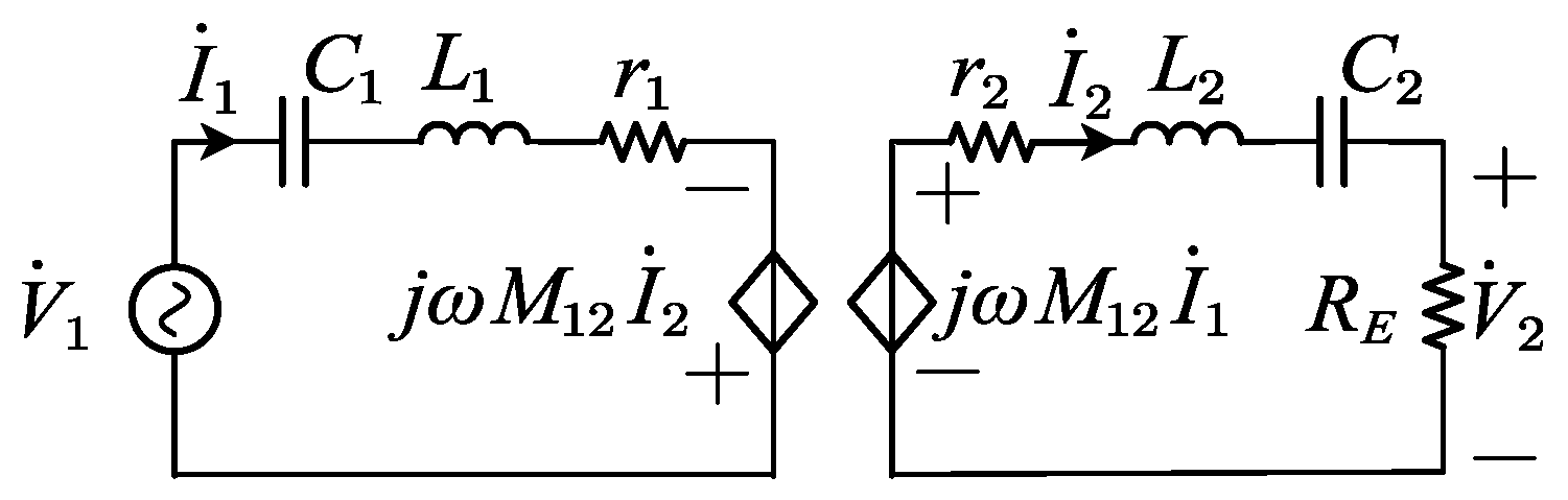
2.1. Multi-Parameter Estimation Model

Figure 1 shows the schematic diagram of the S/S compensated converter, in which Q1~Q4 are power MOSFETs constituting an inverter, D1~D4 are secondary rectifier diodes, and RL is the load resistor. Powered by a DC input voltage, Vin, the inverter produces an AC voltage, v1 (current i1), driving a resonant tank consisting of two compensation capacitors of C1 and C2, two equivalent series resistances of r1, r2, and a coupler. The coupler has a primary inductance, L1, secondary inductance, L2, and mutual inductance, M12. The resonant tank delivers an AC current, i2, which, after being rectified and filtered, gives the DC voltage Vo and current Io. It should be noted that r1 and r2 are the total equivalent series resistances in the primary and secondary circuits, which include the parasitic resistances of L1, C1, L2, C2, and the MOSFETs.
Using the fundamental harmonic approximation, the equivalent circuit of the S/S compensated converter can be obtained, as shown in Figure 2. In the figure, all voltage and current variables are represented by fundamental phasors, and the rectifier is represented by an equivalent resistance RE.
With the help of Fourier analysis, we have
V 1 = 2 2 π V i n , V 2 = 2 2 π V o + 2 V F ,   I 2 = π 2 2 I o
where V1, V2, and I2 stand for the root-mean-square values of the fundamental components of v1, v2, and i2, and VF is the forward voltage drop of the rectifier diode.
Then, RE can be obtained as
R E = V 2 I 2 = 8 π 2 V o + 2 V F I o = 8 π 2 R L + 2 V F I o 8 π 2 R L
Since 2VF/(IoRL) is normally less than 5% for ensuring a high efficiency, the effect of VF on RE can be neglected.
By using Kirchhoff’s voltage law, we have
V 1 0 ° 0 = j X 1 + r 1 j ω M 12 j ω M 12 j X 2 + r 2 + R E I 1 φ I 2 θ
where
X 1 = ω L 1 1 ω C 1 = 1 ω C 1 ω 2 ω p 2 1 , X 2 = ω L 2 1 ω C 2 = 1 ω C 2 ω 2 ω s 2 1
ω represents the operating angular frequency; ωp and ωs are the resonant angular frequencies of Tx and Rx sides, equaling to 1 L 1 C 1 , and 1 L 2 C 2 , respectively; φ and θ are the phase angles for I ˙ 1 and I ˙ 2 , referring to V ˙ 1 .
Expanding the real parts and imaginary parts of (3), yields
X 1 I 1 cos φ + r 1 I 1 sin φ ω M 12 I 2 cos θ = 0 X 1 I 1 sin φ + r 1 I 1 cos φ + ω M 12 I 2 sin θ = V 1 ω M 12 I 1 cos φ X 2 I 2 cos θ ( r 2 + R E ) I 2 sin θ = 0 ω M 12 I 1 sin φ + X 2 I 2 sin θ ( r 2 + R E ) I 2 cos θ = 0
Equations of (2), (4), and (5) provide the fundamental parameter estimation model for the S/S converter. Where, ω is a known parameter determined by the controller of the IPT system; φ, V1, and I1 can be directly measured on the Tx side; C1, C2, and VF can be known prior to charging; L1, L2, M12, r1, Vo, Io, and RL are the parameters that need to be estimated. To facilitate the parameter identification, a primary sensing coil is introduced into the coupler for the detection of θ. As shown in Figure 3, the sensing coil has a self-inductance, L3, mutual inductance, M23, coupling with Rx coil, and mutual inductance, M13, coupling with Tx coil. Adopting a decoupled configuration between Tx and sensing coils, M13 can approximate to zero. Hence, the phase θ of I ˙ 2 can be obtained in Tx side by the open-circuit voltage, V ˙ 3 , across the sensing coil, which satisfies
V ˙ 3 = j ω M 23 I ˙ 2 j ω M 13 I ˙ 1 j ω M 23 I ˙ 2 M 13 0
Further, the phase difference, γ, between i1 and i2 can be obtained. Substituting γ = φθ into (5), yields
r 1 I 1 + ω M 12 I 2 sin γ = V 1 cos φ
X 1 I 1 ω M 12 I 2 cos γ = V 1 sin φ
X 1 I 1 sin γ + r 1 I 1 cos γ = V 1 cos θ
X 2 sin γ ( r 2 + R E ) cos γ = 0
ω M 12 I 1 sin γ ( r 2 + R E ) I 2 = 0
ω M 12 I 1 cos γ X 2 I 2 = 0
The deriving procedure is provided in Appendix A.
Combining (7) and (12) with (4), and eliminating I2 and X2, gives
ω 3 sin 2 γ C 2 2 ω 2 / ω s 2 1 M 12 2 + r 1 = V 1 cos φ I 1
In (13), M12 and r1 are independent of other parameters to be estimated. So, (13) gives a simple identification equation for M12 and r1. Substituting the identified value of M12 and r1 into (7) and (11), the values of I2 and (r2 + RE) can be obtained. Then, according to (2), Vo, Io, and RE can be identified easily. It can be seen that, by introducing the phase difference between i1 and i2, a straightforward, multi-parameter estimation method can be derived.
However, the determination of ωs and the efficient solving of (13) are still two important issues. In order to avoid any limitations on the operating frequency, we propose a frequency-sweeping method so as to obtain ωs and other required information for the solving of (13). By selecting some special points with simplified equations for parameter identification, the solving efficiency can be improved. Thus, the process of the multi-parameter identification comprises two steps. Before charging, a frequency sweeping is performed for the IPT system under weak excitation. As a result, M12, L1, L2, and r1 can be determined prior to charging. During charging, Vo, Io, and RE can be identified rapidly online, based on the obtained parameters during frequency sweeping. At the same time, a Tx-side close-loop control for the IPT system can be realized. The proposed two-step parameter estimation method is suitable for static wireless charging applications, since M12, L1, L2, and r1 do not change during charging.
Next, detailed identifications of the parameters will be described.

2.2. Parameter Estimation during Frequency Sweeping

Firstly, we will discuss how to determine ωs through frequency sweeping.
It can be seen from (6) that V ˙ 3 is 90° ahead of I ˙ 2 when M13 approximates to zero. By frequency sweeping, it is easy to find a frequency at which V ˙ 3 is in the phase of I ˙ 1 , meaning γ = 90°. Substituting γ = 90° into (9) and (10), and combining (4), we have
γ = 90 ° : X 1 = 1 ω C 1 ω 2 ω p 2 1 = V 1 cos θ I 1 ,   X 2 = 1 ω C 2 ω 2 ω s 2 1 = 0
It indicates that the angular frequency, ω, corresponding to γ = 90° is just the secondary resonance frequency, ωs.
Substituting ωs = ω into (14) yields
  γ = 90 ° : ω s = ω ω p = ω I 1 V 1 ω C 1 cos θ + I 1
That means, by detecting the values of ω, Vin, I1, and θ, corresponding to γ = 90°, both ωs and ωp can be obtained.
Then, substituting ωs and ωp into ω p = 1 L 1 C 1 and ω s = 1 L 2 C 2 , L1 and L2 can be calculated.
At last, we will discuss how to solve (13) to identify M12 and r1.
As can be seen from (13), there are two unknown parameters (M12 and r1), but only one equation. During frequency sweeping, multiple sets of variables (ω, γ, φ, V1, and I1) can be measured, ensuring that (13) can be easily solved.
Defining
x 1 ω   = ω 2 sin 2 γ 2 X 2 = ω 3 C 2 sin 2 γ 2 ω 2 / ω s 2 1 , x 2 ω   = V 1 cos φ I 1
Equation (13) can be rewritten as
x 1 ω M 12 2 + r 1 x 2 ω = 0
Equation (17) can be iteratively solved using an optimization algorithm, or directly solved adopting two special cases. We choose the latter for efficient solving. By using two sets of measured variables (ω, γ, φ, V1, and I1) at frequencies ω1 and ω2, the values of M12 and r1 can be solved as
M 12 = x 2 ω 1 x 2 ω 2 x 1 ω 1 x 1 ω 1 r 1 = x 1 ω 2 x 2 ω 1 x 2 ω 2 x 1 ω 1 x 1 ω 2 x 1 ω 1
To facilitate the signal sensing and equation solving, we chose ω1 as the corresponding frequency when v1 is in-phase with i2, i.e., θ = 0, and ω2 as (ω1 + ωs) / 2. Other frequency selections are also feasible. However, the selection of ω1 and ω2 should be avoided around the frequency corresponding to γ = 90° or φ = 90°, near which the slopes of the functions sin2γ and cosφ are relatively large, having a large phase detection error.

2.3. Online Parameter Estimation

Substituting the identified value of M12 and r1 into (7) and (11), we have.
I 2 = V 1 cos φ r 1 I 1 / ω M 12 sin γ
V 2 = R E I 2 = ω M 12 I 1 sin γ 1 + r 2 / R E ω M 12 I 1 sin γ
Normally, r2/RE is less than 3% for achieving a high efficiency. Thus, 1 + r2/RE ≈ 1 in (20).
Substituting (1) into (19) and (20), Vo and Io can be derived
I o = 0 . 81 V i n cos φ 0 . 9 r 1 I 1 ω M 12 sin γ
V o 1.11 ω M 12 I 1 sin γ 2 V F
Since M12, r1, and VF are known parameters, and Vin, I1, φ, γ, and ω can be measured online, the real-time identification of Vo and Io can be realized.
Combining (11) and (12) with (4), gives
R E + r 2 = X 2 tan γ = 1 ω C 2 ω 2 ω s 2 1 tan γ
Combining (23) with (2), RL can be obtained as
R L π 2 8 R E = π 2 8 1 ω C 2 ω 2 ω s 2 1 tan γ
Besides, according to (6), we can calculate the value of M12 online, denoted as M ^ 12 , satisfying
M ^ 12 = 2 sin 2 γ 1 ω 3 C 2 ω 2 ω s 2 1 V 1 cos φ I 1 r 1
According to the value of M ^ 12   and the difference between M ^ 12 and M12, we can judge if the Rx pad is still in the charging region, thereby improving the reliability of the IPT system.

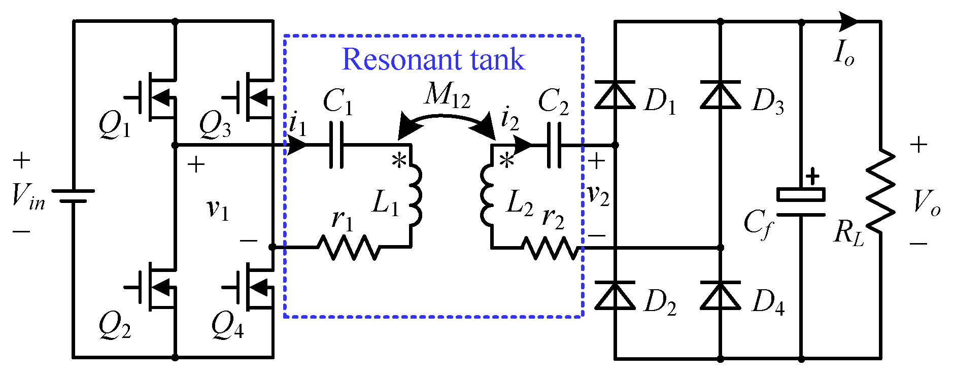
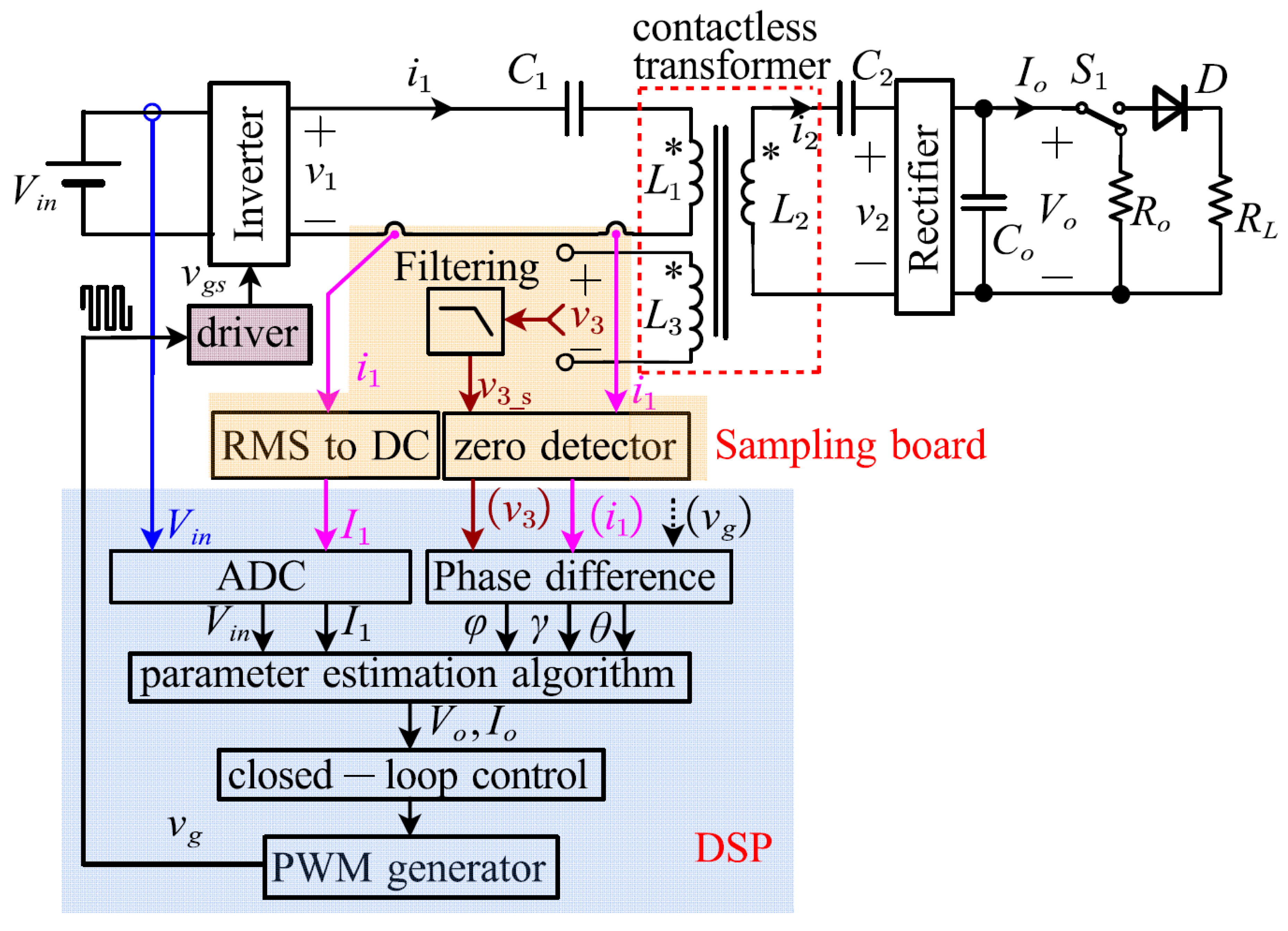
3. Implementation of the Proposed Estimation Method

3.1. Diagram of the IPT System

According to the proposed estimation method in Section 2, the diagram of the IPT system with the Tx-side circuit can be illustrated, as shown in Figure 4, where S1 is used for operating state switching. When S1 is connected with RO, the IPT system will operate in a frequency-sweeping state under weak excitation, for pre-parameter-identification. When S1 is connected with RL, the IPT system will operate in a normal charging state, and the online parameter identification is achieved. As shown in Figure 4, v3 and i3 are converted to square wave signals by the zero detector, to facilitate the detection of φ, θ, and γ. After the parameter estimation, the values of L1, L2, M12, r1, Vo, Io, and RL can be obtained. Based on them, a Tx-side, closed-loop control can be conducted.

3.2. Flowchart of the Parameter Estimation

Figure 5 and Figure 6 illustrate the flowcharts of the proposed parameter estimation algorithm, where the values of γ, φ, θ, Vin, and I1 are measured by the sensors, ω can be obtained by the controller, and V1 can be calculated by (2).
First, the offline parameter estimation is conducted. As shown in Figure 5, ωs and ω1 are obtained by sweeping the operating frequency f from fmin to fmax. The controller measures γ and θ at each frequency, and compares them with 90° and 0°, respectively. When γ = 90°, the corresponding operating frequency is recorded as ωs; when θ = 90°, the corresponding frequency is recorded as ω1. ε is the allowable error. Then, based on ωs and ω1, the operating angular frequency is adjusted, and the three groups of variables (ω, γ, φ, θ, Vin, and I1) are measured at different frequencies to calculate ωp, M12, and r1.
After finishing the offline parameter estimation, the online real-time identification of load variables (Vo, Io, and RL) can be realized, as shown in Figure 6. During the operation, M ^ 12 is estimated and compared with M12 to judge if the Rx pad is in the allowable charging region.
It is worth noting that the proposed estimation method has no operating frequency limitations. Besides, the proposed identification model has considered the effect of r1 and VF, offering high accuracy.

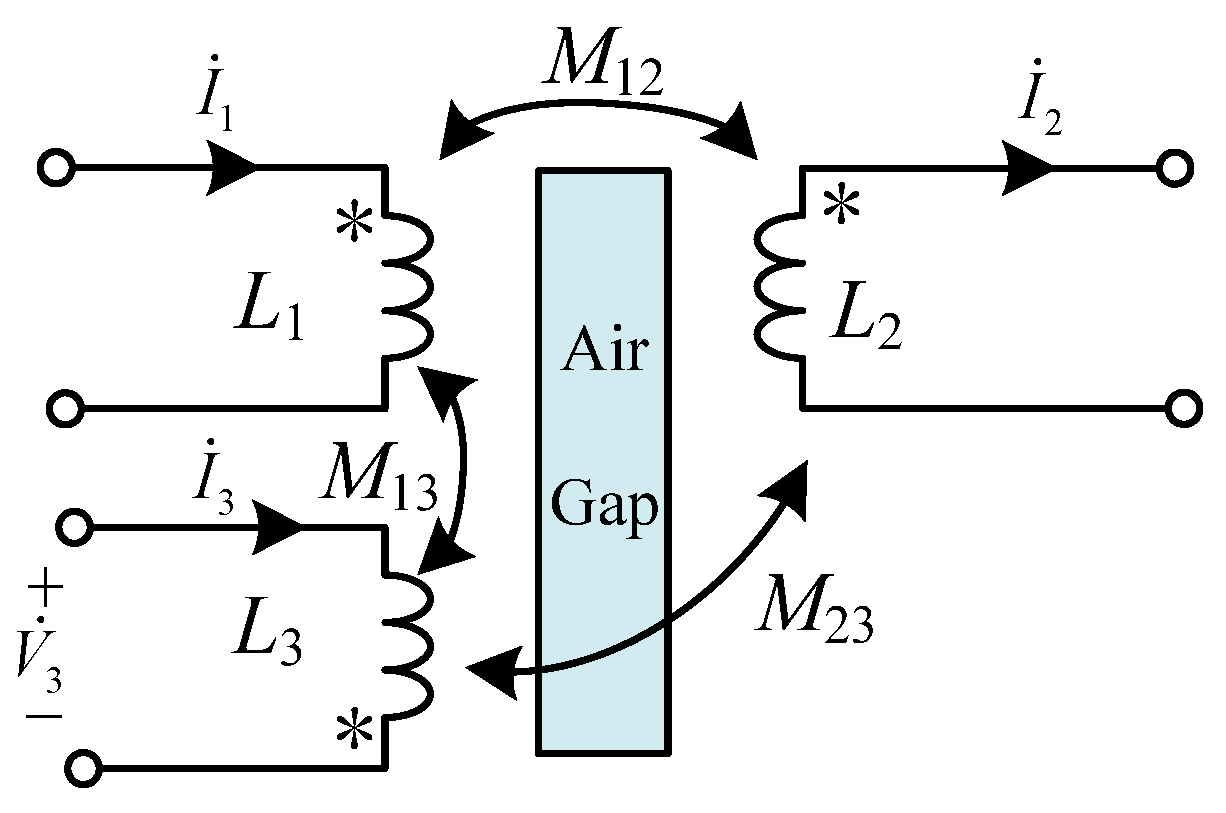
4. Configuration of the Magnetic Coupler

For the IPT system as shown in Figure 4, the contactless transformer is a crucial part, not only for power transfer but also for phase detection of the secondary current. In this section, we will discuss how to determine its configuration.

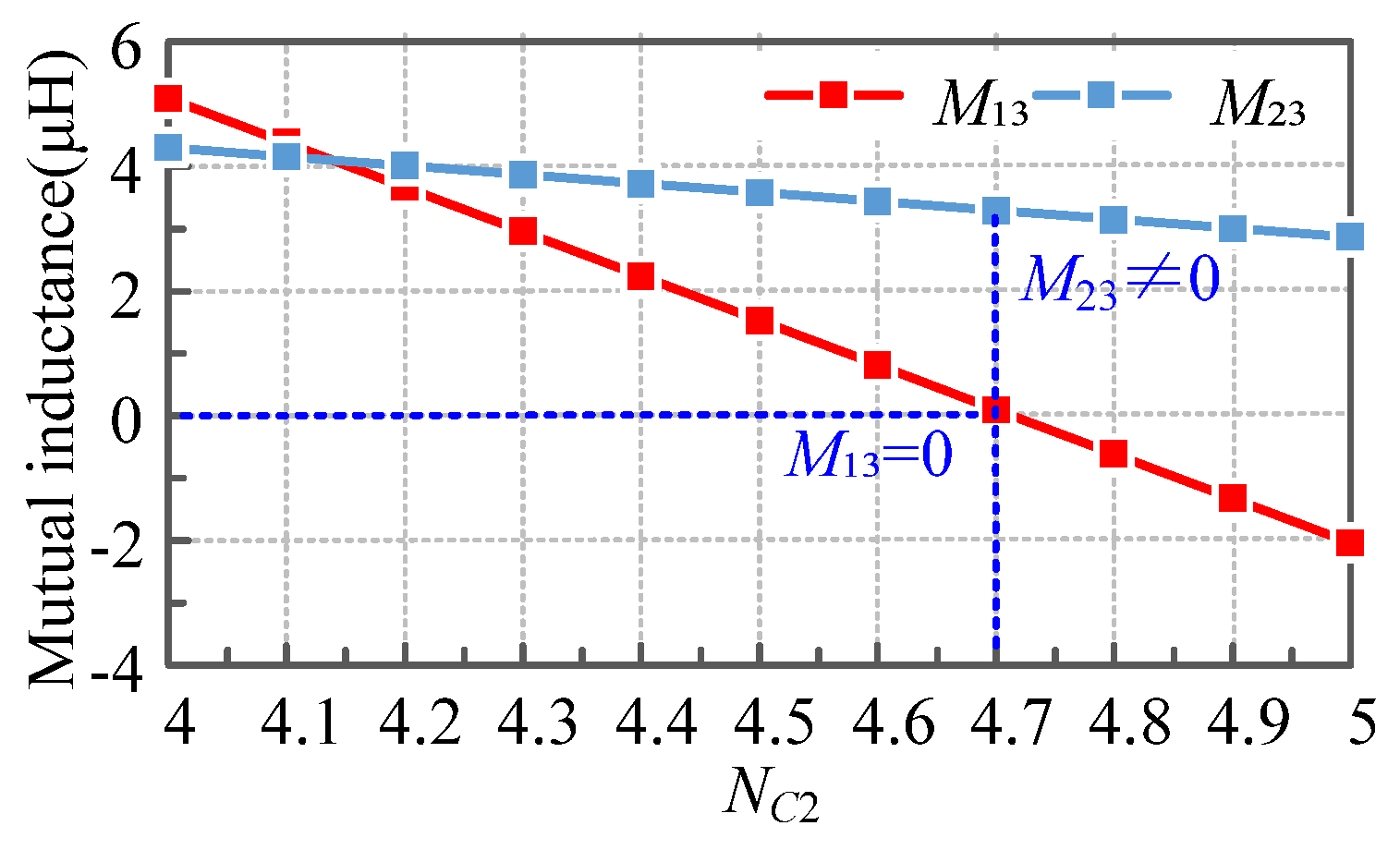
4.1. Proposed Asymmetrical Configuration

As indicated in (6), to realize an accurate phase detection, the contactless transformer is required to have a nearly zero M13 and nonzero M23. That means the sensing coil should always be decoupled with Tx coil and coupled with Rx coil. In previous studies, [25] has presented several decoupled configurations for achieving a nearly zero M13. However, they also make M23 zero when Rx coil is exactly aligned with Tx coil. To satisfy the requirements, an asymmetric structure of the coupler is proposed. As shown in Figure 7, the coupler adopts different sizes for Tx and Rx pads, and the sensing coil is divided into two asymmetric segments, LC1 and LC2.
To obtain the zero coupling (M13 = 0), two sub coils of the sensing coil, LC1 and LC2, are concentrically placed on the Tx pad, and reversely connected in a series. Thus, the equivalent mutual inductance, M13, can be expressed as
M 13 =   N C 1 ϕ C 1 N C 2 ϕ C 2 / i 1
where NC1 and NC2 are the number of turns of LC1 and LC2, and ϕC1 and ϕC2 represent the magnetic flux coupled by LC1 and LC2, respectively. Both ϕC1 and ϕC2 are produced by the Tx coil, and they are the same sign. Then, by adjusting LC1 and LC2, M13 can approach zero.
The asymmetric structure for LC1 and LC2, combining with the different size for Tx and Rx pads, ensures the nonzero M23 under both aligned and misaligned conditions.

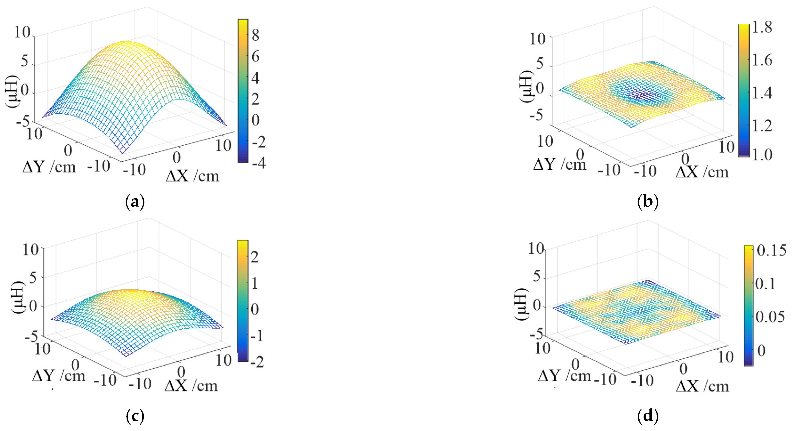
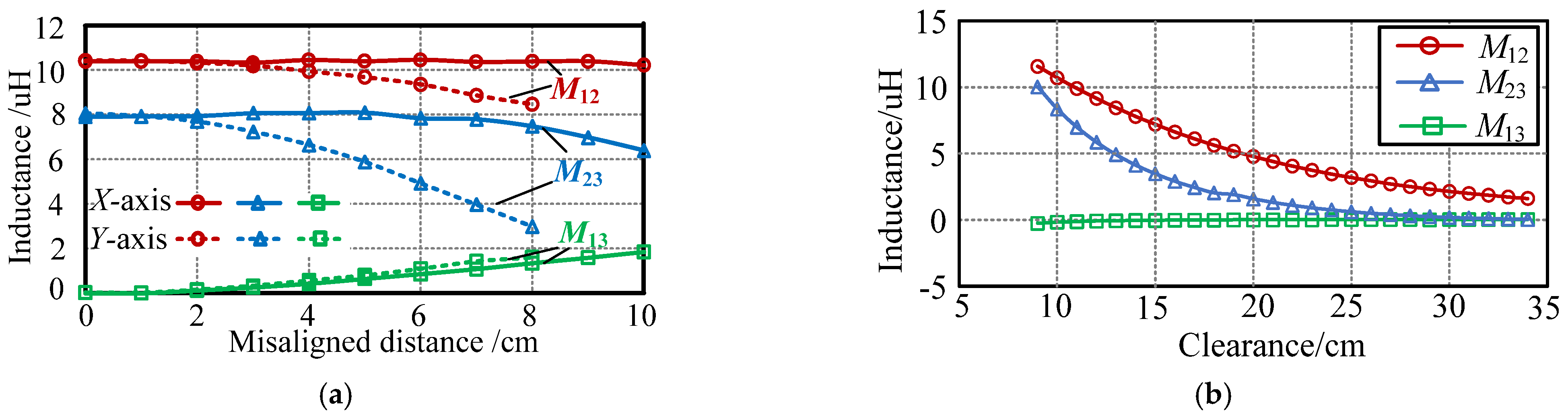
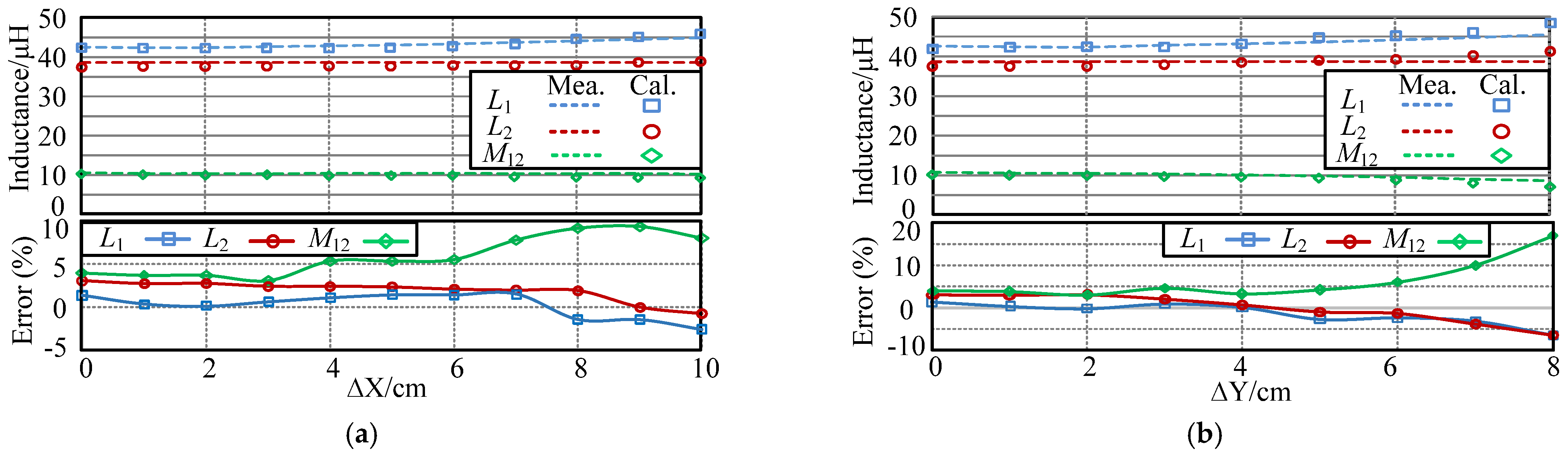
4.2. Simulation Results

We choose the magnetic coupler recommended by SAE J2954-2017 as a design example. Detailed dimensions are as shown in Figure 7, and the clearance, ∆Z, ranges from 10–16 cm.
As shown in Figure 7a, Lc1 is placed around the center of the Tx pad, with six turns for NC1; Lc2 is placed around the outer border of the Tx pad with NC2 turns. By measuring the mutual inductance with an LCR meter, we can easily find a proper value for NC2 to achieve a zero M12. The practical configuration of the sensing coil is shown in Figure 7c. As seen, NC2 is about 4.7 since the outermost turn of Lc2 is not fully wound.
We also use the software COMSOL to assist the design of the sensing coil. Figure 8 shows the curves of M13 and M23 versus NC2. It can be seen that zero coupling (M13 = 0) occurs at the point of NC2 = 4.7, which also guarantees a nonzero M23. When Tx and Rx pads are aligned, due to the asymmetrical configurations of the coupler and the sensing coil, the couplings between Lc1/ Lc2 and Rx coil will not be completely offset, yielding a nonzero M23. Besides, the simulated value of NC2 (4.7) for M13 = 0 matches the measured one very well.
Using NC1 = 6 and NC2 = 4.7, M13 and M23 are further simulated in the case of misalignments, as shown in Figure 9. It can be seen that M13 is close to zero and M23 is larger than zero within a wide range of misalignments, meeting the coupling requirements. Therefore, the proposed asymmetric configuration is suitable for phase detection.
Since the sensing coil is mounted on the Tx pad, M13 is a constant, while M23 is a parameter sensitive to the relative position between Tx coil and Rx coil. As shown in Figure 9, M23 gradually decreases with increasing ∆X and ∆Y. When M23 is reduced to zero, the sensing coil will lose the function for the phase detection, which should be avoided. Figure 10 illustrates the simulated zero coupling position of M23. The radius of the effective coupling area is approximately 10 cm, satisfying the misalignment requirements (∆X ≤ ±7.5 cm and ∆Y ≤ ±10 cm) by the SAE J2954 standard.

5. Experimental Evaluation and Discussion

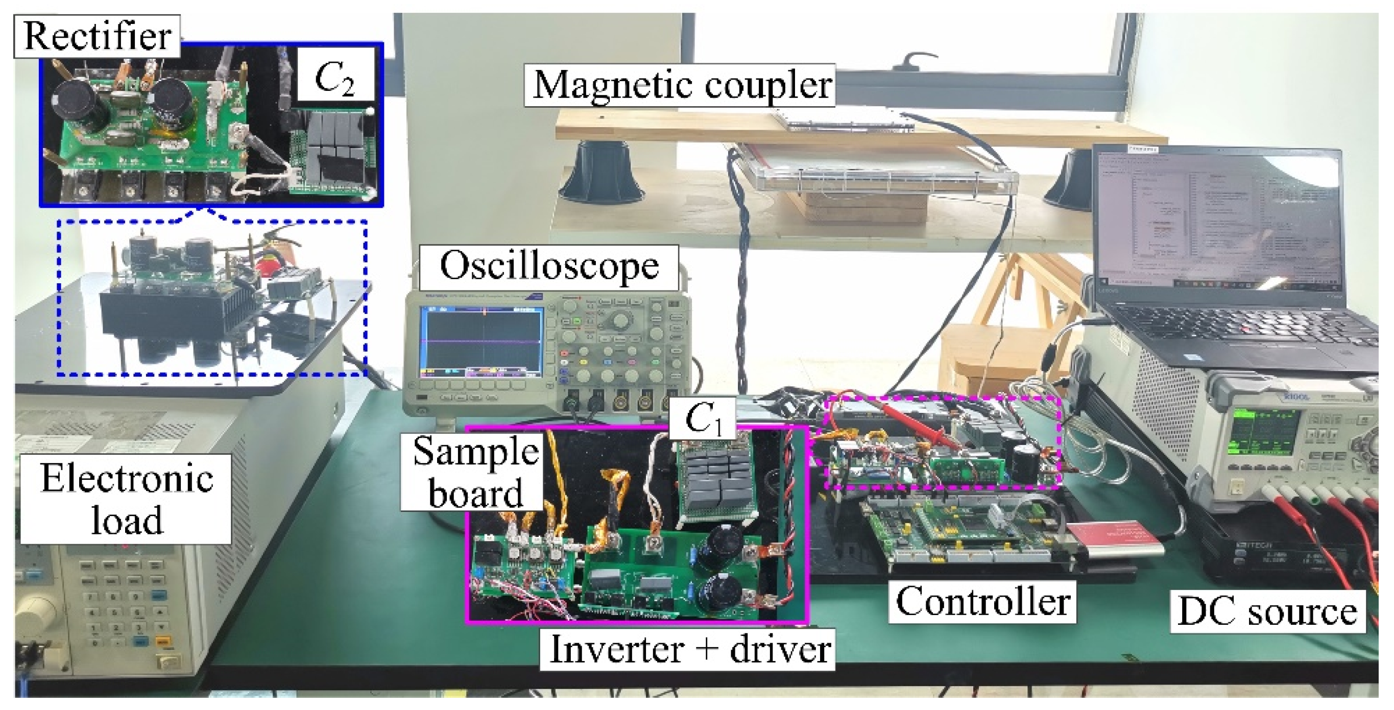
5.1. Experimental Prototype

To verify the above analysis, a 1 kW prototype was built and tested in the laboratory. Figure 11 shows the experimental setup for the built prototype. The system parameters are listed in Table 2. The variable frequency range is from 85 kHz to 100 kHz. Q1~Q4 are IXTV200N10T (RDS(ON) = 5.5 mΩ) and D1~D4 are DSEI120-06A (VF = 0.7 V). The parameter estimation method and the closed-loop control are implemented in the DSP TMS320F28335 (150 MHz).
The experimental verifications include three parts: (1) the verification of the phase-detection function; (2) the feasibility and accuracy of the proposed parameter estimation method; (3) the transmitter-side, closed-loop control with the estimated results.

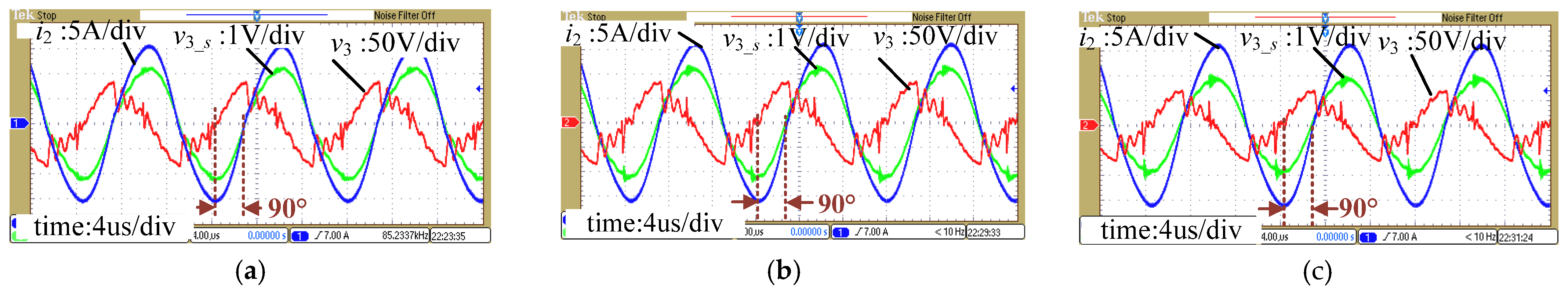
5.2. Phase Detection of the Secondary Current

The practical inductances and coil resistances (rL1, rL2, and rL3) of the proposed magnetic coupler are listed in Table 3. Figure 12 illustrates the variation of M12, M23, and M13 under misalignments and different clearance conditions. As expected, M13 is approximately zero within the required clearance range and a certain range of misalignments, while M23 is greater than zero, satisfying the coupling requirements discussed in Section 4.
To verify the phase-detection function of the sensing coil, the experimental waveforms of v3, its filtered output, v3_s, and i2, are tested with different misalignments. As shown in Figure 13, v3 is distorted. To correct this distortion, a low-frequency filter with a 90° phase shift is adopted. In the waveforms, v3_s and i2 are always in-phase, and lag, v3, is nearly 90°, agreeing with the theoretical analysis in (6). Therefore, the presented asymmetrical configuration of the coupler can accurately detect the phase information of i2.

5.3. Parameter Estimation Results

5.3.1. Offline Parameter Estimation

Offline parameter estimation is conducted under weak excitation with Vin = 30 V. Relay S1 in Figure 4 is switched to the test resistor Ro, and Ro is fixed at 8 Ω during the estimation process. Following the procedure provided in Figure 5, M12, L1, L2, and r1 are obtained, as illustrated in Table 4 and Figure 14.
Note that r1 represents the total equivalent resistance in the transmitter circuit, and its measured value is calculated as the sum of rL1, rC1, and RDS(ON).
r 1 _ mea 2 R D S O N + r L 1 + r C 1 = 117.2   m Ω
To evaluate the accuracy of the estimation, the estimation error is defined as
ε =   Mea . Cal . / Mea . × 100 %
where Mea. and Cal. represent the measured and calculated values, respectively.
It can be seen from Table 4 that the ε for M12, L1, and L2 are all less than 4%, indicating the high accuracy of the estimation method. However, the ε for r1 is much larger. From (27), it can be noted that r1 is only 117.2 mΩ. Thus, a small deviation will lead to a large error.
Figure 14 shows that the estimation accuracy is lower when the misaligned distance is relatively large. Hence, the misalignment should be set within a suitable range, to ensure estimation accuracy. Within the misaligned range of ∆X ≤ 6 cm and ∆Y ≤ 6 cm, the maximum identification error of M12 is 5.5%, the maximum identification error of L1 is 3.9%, and the maximum identification error of L2 is 3.6%.

5.3.2. Online Parameter Estimation

With the estimated M12, L1, L2, and r1, the online parameter estimation is carried out based on the estimation method in Figure 6. The relative position of the Tx coil and the Rx coil is fixed at (∆X = 0 cm, ∆Y = 0 cm, and ∆Z = 10 cm).
Figure 15 shows the measured and estimated values of Vo and Io at various frequencies and load resistances. The frequency is changed from 85 kHz to 105 kHz, and Ro is varied from 6 Ω to 16 Ω. All the identification results are in good agreement with the measured ones, and the maximum ε is less than 8%. The feasibility and accuracy of the proposed identification method are well verified.
The online estimated values of M12 with different Ro are illustrated in Figure 16. The measured value (10.62 μH) and the offline estimated value (10.2 μH) are also marked in Figure 16 for comparison. As seen, the estimated M ^ 12 varies around M12. Therefore, by comparing M ^ 12 with M12, it can be detected whether there is abnormal movement during charging.
Figure 17 shows the identification results of RL. The switching frequency is fixed at 85 kHz, and RL is changed from 4 to 20 Ω. The estimated results coincide with the theoretical results, verifying the effectiveness of the proposed estimation method.

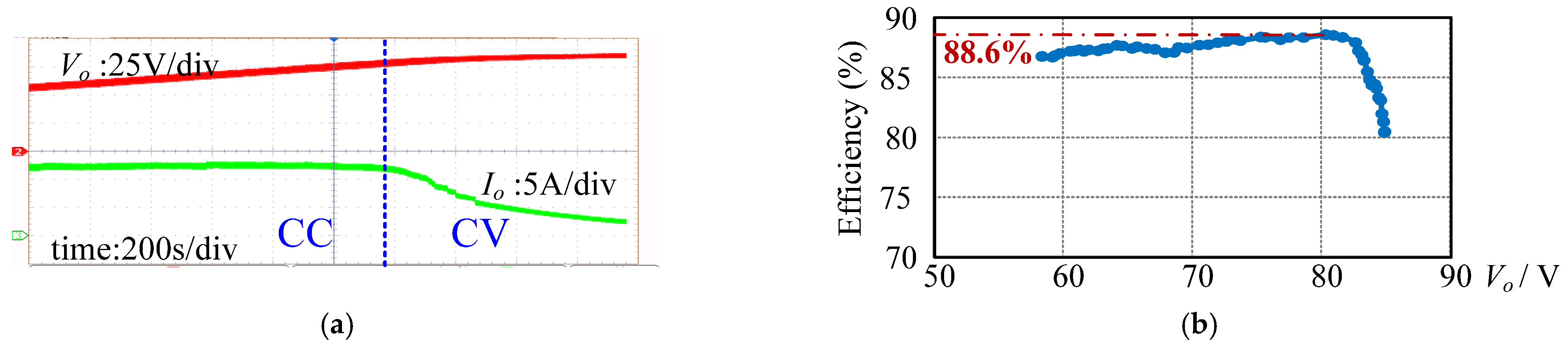
5.4. Closed-Loop Control Results

Based on the dynamically estimated values of Vo and Io, constant current (CC) and constant voltage (CV) charging for S/S compensation are also achieved by employing only a transmitter controller. Here, the variable frequency control is employed. The operating frequency range is set as 85 kHz–100 kHz. The calculation time for Io and Vo are listed in Table 5. As seen, the calculation time is smaller than the switching period. So, Vo and Io can be identified rapidly during charging.
In the prototype, a bidirectional, programmable DC power supply of IT6006C-500-40 is used to imitate the characteristics of the battery. The parameters of the battery emulator are set as follows: an empty voltage of 56 V, a full voltage of 80 V, a negative/positive current limit value of 20 A, and an inner resistance of 10 mΩ. The target charging current for CC mode is set as 13 A. The battery-charging waveforms of Vo and Io, and the measured efficiency, are shown in Figure 18. As seen in Figure 18a, both CC charging and CV charging are achieved. It demonstrates the effectiveness of the proposed parameter estimation method. The maximum efficiency is 88.6%.

6. Conclusions

In this paper, a multi-parameter estimation method that utilizes the phase difference between primary and secondary currents is proposed for an S/S compensated contactless converter. This method has the advantages of generality, i.e., being without operating frequency limitation, and having high accuracy and identification efficiency, which is suitable for transmitter-side, real-time control. The detailed implementation of the parameter estimation method is studied. For realizing precise phase detection of the secondary current, a novel structure, which divides the sensing coil into two asymmetrical segments, is presented. A 1 kW wireless charger prototype is built for verification. The estimated results and the actual values are in close agreement, and the maximum identification error is less than 8%. Also, a closed-loop control is performed based on the estimated results.

Author Contributions

Conceptualization, L.X. and G.K.; methodology, L.X. and G.K.; software, B.Z.; validation, L.X., G.K. and Q.C.; formal analysis, L.X.; investigation, L.X. and G.K.; resources, Q.C., X.R. and Z.Z.; writing—original draft preparation, L.X. and G.K.; writing—review and editing, Q.C., X.R. and Z.Z.; supervision, Q.C.; project administration, L.X.; funding acquisition, L.X. and Q.C. All authors have read and agreed to the published version of the manuscript.

Funding

This work was supported by Jiangsu Provincial Industrial Prospective and the Key Core Technology Project of China, grant number BE2019113.

Conflicts of Interest

The authors declare no conflict of interest.

Appendix A

For clarity, the formulas in (5) are renumbered follows:
X 1 I 1 cos φ + r 1 I 1 sin φ ω M 12 I 2 cos θ = 0
X 1 I 1 sin φ + r 1 I 1 cos φ + ω M 12 I 2 sin θ = V 1
ω M 12 I 1 cos φ X 2 I 2 cos θ ( r 2 + R E ) I 2 sin θ = 0
ω M 12 I 1 sin φ + X 2 I 2 sin θ ( r 2 + R E ) I 2 cos θ = 0
Multiplying (A1) by sinφ and (A2) by cosφ, and then adding them up, gives
r 1 I 1 sin 2 φ + cos 2 φ   +   ω M 12 I 2 sin θ cos φ cos θ sin φ   = V 1 cos φ r 1 I 1 + ω M 12 I 2 sin θ φ   = V 1 cos φ
Substituting γ = φθ into (A5) yields (7).
Similarly, (8) can be derived by adding the product of (A1) and cosφ with the product of (A2) and (−sinφ), that is
X 1 I 1 cos 2 φ + sin 2 φ   ω M 12 I 2 cos θ cos φ + sin θ sin φ   = V 1 sin φ X 1 I 1 ω M 12 I 2 cos θ φ   = V 1 sin φ X 1 I 1 ω M 12 I 2 cos γ = V 1 sin φ   ( 8 )
A 1 sin θ + A 2 cos θ gives (9).
X 1 I 1 cos φ sin θ sin φ cos θ   +   r 1 I 1 sin φ sin θ + cos φ cos θ   = V 1 cos θ X 1 I 1 sin θ φ + r 1 I 1 cos θ φ   = V 1 cos θ X 1 I 1 sin γ + r 1 I 1 cos γ = V 1 cos θ   ( 9 )
The derivations (10)–(12) follow a likewise procedure and are omitted in this paper.

References

  1. Covic, G.A.; Boys, J.T. Inductive Power Transfer. Proc. IEEE 2013, 101, 1276–1289. [Google Scholar] [CrossRef]
  2. Cheng, Z.; Lei, Y.; Song, K.; Zhu, C. Design and Loss Analysis of Loosely Coupled Transformer for an Underwater High-Power Inductive Power Transfer System. IEEE Trans. Magn. 2015, 51, 1–10. [Google Scholar]
  3. Ho, J.S.; Kim, S.; Poon, A.S.Y. Midfield Wireless Powering for Implantable Systems. Proc. IEEE 2013, 101, 1369–1378. [Google Scholar] [CrossRef]
  4. Zhang, L.; Gu, S.J.S.; Huang, X.; Palmer, J.; Giewont, W.; Wang, F.; Tolbert, L.M. Design Considerations for High-Voltage Insulated Gate Drive Power Supply for 10-kV SiC MOSFET Applied in Medium-Voltage Converter. IEEE Trans. Ind. Electron. 2021, 68, 5712–5724. [Google Scholar] [CrossRef]
  5. Ahmad, A.; Alam, M.S.; Chabaan, R. A Comprehensive Review of Wireless Charging Technologies for Electric Vehicles. IEEE Trans. Transp. Electrification 2018, 4, 38–63. [Google Scholar] [CrossRef]
  6. Patil, D.; McDonough, M.K.; Miller, J.M.; Fahimi, B.; Wireless, P.T.B. Power Transfer for Vehicular Applications: Overview and Challenges. IEEE Trans. Transp. Electrification 2018, 4, 3–37. [Google Scholar] [CrossRef]
  7. Hsu, J.U.W.; Hu, A.P.; Swain, A. A Wireless Power Pickup Based on Directional Tuning Control of Magnetic Amplifier. IEEE Trans. Ind. Electron. 2009, 56, 2771–2781. [Google Scholar] [CrossRef]
  8. Beh, T.C.; Kato, M.; Imura, T.; Oh, S.; Hori, Y. Automated Impedance Matching System for Robust Wireless Power Transfer via Magnetic Resonance Coupling. IEEE Trans. Ind. Electron. 2013, 60, 3689–3698. [Google Scholar] [CrossRef]
  9. Huang, Z.; Lam, C.-S.; Mak, P.-I.; Martins, R.P.d.; Wong, S.-C.; Tse, C.K. A Single-Stage Inductive-Power-Transfer Converter for Constant-Power and Maximum-Efficiency Battery Charging. IEEE Trans. Power Electron. 2020, 35, 8973–8984. [Google Scholar] [CrossRef]
  10. Colak, K.; Asa, E.; Bojarski, M.; Czarkowski, D.; Onar, O.C. A Novel Phase-Shift Control of Semibridgeless Active Rectifier for Wireless Power Transfer. IEEE Trans. Power Electron. 2015, 30, 6288–6297. [Google Scholar] [CrossRef]
  11. Li, H.; Wang, K.; Fang, J.; Tang, Y. Pulse Density Modulated ZVS Full-Bridge Converters for Wireless Power Transfer Systems. IEEE Trans. Power Electron. 2019, 34, 369–377. [Google Scholar] [CrossRef]
  12. Li, H.; Fang, J.; Chen, S.; Wang, K.; Tang, Y. Pulse Density Modulation for Maximum Efficiency Point Tracking of Wireless Power Transfer Systems. IEEE Trans. Power Electron. 2018, 33, 5492–5501. [Google Scholar] [CrossRef]
  13. Jiang, Y.; Wang, L.; Wang, Y.; Wu, M.; Zeng, Z.; Liu, Y.; Sun, J. Phase-Locked Loop Combined With Chained Trigger Mode Used for Impedance Matching in Wireless High Power Transfer. IEEE Trans. Power Electron. 2020, 35, 4272–4285. [Google Scholar] [CrossRef]
  14. Yeo, T.D.; Kwon, D.; Khang, S.T.; Yu, J.W. Design of Maximum Efficiency Tracking Control Scheme for Closed-Loop Wireless Power Charging System Employing Series Resonant Tank. IEEE Trans. Power Electron. 2017, 32, 471–478. [Google Scholar] [CrossRef]
  15. Wang, Z.H.; Li, Y.P.; Sun, Y.; Tang, C.S.; Lv, X. Load Detection Model of Voltage-Fed Inductive Power Transfer System. IEEE Trans. Power Electron. 2013, 28, 5233–5243. [Google Scholar] [CrossRef]
  16. Hu, S.; Liang, Z.; Wang, Y.; Zhou, J.; He, X. Principle and Application of the Contactless Load Detection Based on the Amplitude Decay Rate in a Transient Process. IEEE Trans. Power Electron. 2017, 32, 8936–8944. [Google Scholar] [CrossRef]
  17. Thrimawithana, D.J.; Madawala, U.K. A primary side controller for inductive power transfer systems. In Proceedings of the 2010 IEEE International Conference on Industrial Technology, Via del Mar, Chile, 14–17 March 2010. [Google Scholar]
  18. Su, Y.G.; Zhang, H.Y.; Wang, Z.H.; Hu, A.P.; Chen, L.; Sun, Y. Steady-State Load Identification Method of Inductive Power Transfer System Based on Switching Capacitors. IEEE Trans. Power Electron. 2015, 30, 6349–6355. [Google Scholar] [CrossRef]
  19. Liu, Y.; Madawala, U.K.; Mai, R.; He, Z. Primary-Side Parameter Estimation Method for Bi-Directional Inductive Power Transfer Systems. IEEE Trans. Power Electron. 2021, 36, 68–72. [Google Scholar] [CrossRef]
  20. Liu, F.; Chen, K.; Zhao, Z.; Li, K.; Yuan, L. Transmitter-Side Control of Both the CC and CV Modes for the Wireless EV Charging System With the Weak Communication. IEEE J. Emerg. Sel. Top. Power Electron. 2018, 6, 955–965. [Google Scholar] [CrossRef]
  21. Yin, J.; Lin, D.; Parisini, T.; Hui, S.Y. Front-End Monitoring of the Mutual Inductance and Load Resistance in a Series–Series Compensated Wireless Power Transfer System. IEEE Trans. Power Electron. 2016, 31, 7339–7352. [Google Scholar] [CrossRef]
  22. Dai, X.; Sun, Y.; Tang, C.; Wang, Z.; Su, Y.; Li, Y. Dynamic parameters identification method for inductively coupled power transfer system. In Proceedings of the 2010 IEEE International Conference on Sustainable Energy Technologies (ICSET), Kandy, Sri Lanka, 6–9 December 2010. [Google Scholar]
  23. Chow, J.P.-W.; Chung, H.-H.; Cheng, C.-S.; Wang, W. Use of Transmitter-Side Electrical Information to Estimate System Parameters of Wireless Inductive Links. IEEE Trans. Power Electron. 2017, 32, 7169–7186. [Google Scholar] [CrossRef]
  24. Chow, J.P.W.; Chung, H.S.H.; Cheng, C.S. Use of Transmitter-Side Electrical Information to Estimate Mutual Inductance and Regulate Receiver-Side Power in Wireless Inductive Link. IEEE Trans. Power Electron. 2016, 31, 6079–6091. [Google Scholar] [CrossRef]
  25. Xu, L.; Chen, Q.; Ren, X.; Wong, S.C.; Tse, C.K. Self-Oscillating Resonant Converter With Contactless Power Transfer and Integrated Current Sensing Transformer. IEEE Trans. Power Electron. 2017, 32, 4839–4851. [Google Scholar] [CrossRef]
Figure 1. S/S compensated converter.
Electronics 11 01023 g001
Figure 2. Equivalent circuit of the S/S compensated converter.
Electronics 11 01023 g002
Figure 3. Contactless transformer with a primary sensing coil.
Electronics 11 01023 g003
Figure 4. Diagram of IPT system with Tx- side circuit.
Electronics 11 01023 g004
Figure 5. Flowchart of the off-line parameter estimation.
Electronics 11 01023 g005
Figure 6. Flowchart of the online parameter estimation.
Electronics 11 01023 g006
Figure 7. Asymmetric structure and dimensions of the coupler. (a) Two-dimensional graph of Tx pad, (b) three-dimensional graph of the coupler, and (c) practical configuration of the sensing coil.
Electronics 11 01023 g007
Figure 8. Simulated M13 and M23 versus NC2 (∆X = ∆Y = 0 and ∆Z = 13 cm).
Electronics 11 01023 g008
Figure 9. Simulated M13 and M23 under different misalignments at ∆Z = 10 cm: (a) M23 and (b) M13. At ∆Z = 16 cm: (c) M23 and (d) M13.
Electronics 11 01023 g009
Figure 10. Zero coupling position of M23 at a clearance of (a) ∆Z = 10 cm and (b) ∆Z = 16 cm.
Electronics 11 01023 g010
Figure 11. Photo of the prototype.
Electronics 11 01023 g011
Figure 12. Measured mutual inductances of M12, M23, and M13 under (a) misaligned conditions with ∆Z = 10 cm and (b) different clearance conditions with ∆X = ∆Y = 0 cm.
Electronics 11 01023 g012
Figure 13. Experimental waveforms of v3, v3_s, and i2 under the condition of (a) ∆X = ∆Y = 0 cm; (b) ∆X = 0 cm and ∆Y = 6 cm; (c) ∆X = 4 cm and ∆Y = 0 cm. (∆Z = 10cm).
Electronics 11 01023 g013
Figure 14. Experimental results for the off-line estimation versus (a) ∆X; (b) ∆Y.
Electronics 11 01023 g014
Figure 15. Identification results of the (a) output voltage and (b) output current at various frequencies and load resistances.
Electronics 11 01023 g015
Figure 16. Online mutual inductance estimation results at different loads.
Electronics 11 01023 g016
Figure 17. Identification results of the load resistance, RL.
Electronics 11 01023 g017
Figure 18. (a) Charging curves for closed-loop control and (b) corresponding efficiencies.
Electronics 11 01023 g018
Table 1. Main transmitter-side parameter estimation methods.
Parameter Identification MethodsCompensationsIdentified VariablesOperating FrequencyRef.
Transient modelFree oscillation damping modelS/SRL (>50 Ω)Self-oscillating frequency[15]
RL (<25 Ω)Self-oscillating frequency[16]
Steady-state modelPhasor analysisLCL/PVo and MFixed at resonant frequency[17]
S/SRL and MTracking primary resonant frequency[18]
MFrequency with zero input phase angle[19]
M, r2Fixed at resonant frequency[20]
RL and MDifferent from ω2[21]
Energy conservationS/SReflected impedanceFixed at resonant frequency[22]
Curve fittingS/SM and equivalent loadFixed at resonant frequency[23]
Q1, Q2, ω1, ω2, L1, L2, and k/[24]
Note: Vo is the output voltage and RL is the load resistance. M and k represent the mutual inductance and the coupling coefficient between the transmitting and receiving coils. r2 is the parasitic resistance of the secondary coil. L1, L2, Q1, and Q2 represent the self-inductances and quality factors of the two coils of the coupler, respectively. ω1 and ω2 represent the resonant frequencies of the transmitter and the receiver, respectively.
Table 2. IPT prototype parameters.
ComponentsValueComponentsValue
Input voltage80 VOutput power1 kW
Resonant frequency85 kHzCompensationC1 = 88.1 nF, rC1 = 41.2 mΩ
Clearance range10–16 cmC2 = 94.5 nF, rC1 = 27.4 mΩ
Table 3. Measured parameters of the magnetic coupler.
∆ZL1/μHL2/μHL3/μHM12/μHM13/μHM23/μHrL1rL2rL3
10 cm42.5638.6647.2610.620.1658.360.0650.060.28
13 cm44.0737.5246.58.4550.064.92
16 cm44.9736.746.256.6350.0152.915
Table 4. Estimated results of M12, L1, L2, and r1 at different clearances.
∆ZEstimated ResultsEstimation Error ε
L1/μHL2/μHM12/μHr1L1/μHL2/μHM12/μHr1
10 cm41.9837.4810.20.156−1.3%−3.05%−3.95%33.1%
13 cm43.6137.088.1620.15−1.04%−1.17%−3.47%27.9%
16 cm44.5236.416.7090.147−1%−0.08%−1.12%25.4%
Table 5. Calculation time for Io and Vo (TMS320F28335 150 MHz).
Execution CycleCalculation Time
Vo3462.30667 μs
Io1781.18667 μs
Publisher’s Note: MDPI stays neutral with regard to jurisdictional claims in published maps and institutional affiliations.

