Article

A Simple Method to Design a UWB Filter with a Notched Band Using Short-Circuit Step Impedance Stubs

1
School of Mechatronics and Information Engineering, Putian University, Putian 351100, China
2
Bachelor Program in Advanced Materials, Department of Materials Engineering, National Pingtung University of Science and Technology, Pingtung 91201, Taiwan
3
Graduate Institute of Materials Engineering, National Pingtung University of Science and Technology, Pingtung 91201, Taiwan
*
Author to whom correspondence should be addressed.
Electronics 2022, 11(7), 1124; https://doi.org/10.3390/electronics11071124
Submission received: 22 August 2021 / Revised: 7 March 2022 / Accepted: 14 March 2022 / Published: 1 April 2022
(This article belongs to the Special Issue Emerging Research in Microwave Systems and Applications)

Abstract

:
This article presents a simple method to design an ultra-wideband (UWB) bandpass filter (BPF) with a notched band. The structure of the filter is simple and is composed of a single half-wavelength resonator loaded with three sets of short-circuit step impedance stubs. An equivalent circuit model is presented to analyze the resonance characteristics. Compared with the traditional quarter-wavelength uniform impedance stub, the novelty of the short-circuit step impedance stub introduces two design parameters: the impedance ratio (K) and the electrical length ratio (α). Therefore, by adjusting these design parameters, the frequencies of the first two notched bands can be tuned widely, so a wide frequency band with a notched band can easily be achieved. With a K of 0.36 and an α of 0.6, the designed filter achieved an ultra-wideband bandpass response with a notched band. The UWB response had a passband range of 2.5 GHz–10.5 GHz and a notched band around 5.1 GHz with an attenuation of about 45 dB. The insertion loss in the entire passband was less than 1.26 dB, and the return loss was larger than 10 dB on average. The maximum group delay variation in the two passbands was less than 0.3 nS. The measurement results showed good agreement with the simulation results.

1. Introduction

With the development of wireless communication technology, research into radio frequency bandpass filters (BPF) has become an important development direction [1,2]. The study of wideband components has subsequently become one of the current hot spots. In the past, several resonator structures were proposed to achieve an ultra-wideband (UWB) filter design [3,4,5,6,7,8,9,10,11,12,13,14], such as a step impedance resonator (SIR) [3,4], a stub loaded resonator (SLR) [5,6,7,8], a defected ground structure (DGS) [9], a multilayer structure [10], a substrate integrated waveguide structure (SIW) [11,12], etc. In [3], compact wideband BPFs with high selectivity and wide stopbands were designed using typical SIR. In [4], an SLR and an SIR were used to control the impedance ratio and the length of the stub to obtain dual-band responses with the transmission zeros, bandwidth control, and size reduction through the folded structure. In [5], a multimode SLR was used for wideband BPFs, which have good in-band and out-of-band performances but have a large circuit size and experience insertion loss. In [6], a wideband BPF with a notched band was designed using a resonant cavity loaded by a stub, but the design process and structure were complicated. In [7], a compact UWB BPF was proposed using open/short stub loading to improve the upper stopband. In [8], a wideband BPF design was implemented by DGS, but the destruction of the ground plane of the DGS caused signal incompleteness. In [9], a new type of UWB BPF based on a square patch resonator with slot grounding was proposed. Due to this special geometric structure, the three basic resonators of the resonant cavity were independently controlled, and a UWB passband could be formed. In [10], the multilayer structure UWB filter with an adjustable notch bandwidth proposed was composed of two curved T-shaped microstrip patches on the top and bottom layers and a circular coupling groove in the middle layer. The multilayer structure led to a compact size and tight coupling characteristics. Recently in [11], a half-mode SIW with three resonant modes was also used to generate a wideband response. In [12], a single sector substrate integrated waveguide (SSIW) with a significantly small angle of 2.2° was proposed and designed for a dual-mode UWB BPF with further miniaturized size. Moreover, in [13], an outstanding hybrid design technique including a typical series LC circuit, a miniaturizing inductor, and two transmission lines were used to reduce the size and improve the performance of a microstrip Wilkinson power divider, leading to a 100% reduction in size, the suppression of an infinite number of harmonics, and high-frequency selectivity. In [14], artificial intelligence technology was used to design a compact power divider with squared resonators. This technique always achieves a good frequency band selectivity and miniaturized filters without the use of a complicated design process.
In fact, the most traditional lowpass filters use a uniform 50 Ω transmission line loaded with multiple identical symmetrical quarter-wavelength short-circuit stubs [15]. This structure is simple and makes it easy to predict the characteristics. In recent years, there has been some research that has aimed to optimize the characteristics of this structure. In [16], five quarter-wavelength short-circuit stubs were added on the half-wavelength step impedance microstrip line to improve the selectivity of the designed UWB filter. However, the circuit size was quite large since five stubs were required to achieve the desired selectivity and the notch band was hard to implement in the design. In [17], a notched UWB filter was presented using a stepped impedance stub loaded with a microstrip resonator and spurlines. However, the effect of the impedance ratio (K) on the filter response was not clearly discussed in the paper and the extra structure of the spurlines was needed to create the notch band. In [18], a Chebyshev quarter-wavelength wideband filter was proposed by adding quarter-wavelength open-circuit stubs on uniform 50 Ω transmission lines with magnetic coupling to the defective ground of a dumbbell ring resonator. However, it degraded the signal integration of the ground plane with the defective ground. In [19], a UWB BPF was designed using an exponential tapered high impedance line stub loaded microstrip resonator. With inductive loading on a quarter-wavelength stub, a sharp notch stopband was exhibited around 5.5 GHz with an attenuation level of 30 dB. However, the analysis of the exponential tapered high impedance line stub was complex and hard to fabricate.
This paper presents a simple method to design a UWB BPF with a notched band. Figure 1 shows the structure for the designed UWB BPF with a notched band. The structure of the filter is very simple. It consists of a half-wavelength microstrip resonator loaded with three sets of short-circuit step impedance stubs, one of which is at the center, and the two others are on the other side symmetrically. The input and output end are directly taped to the single half-wavelength resonator to provide sufficient coupling energy to realize the wideband response. Two design parameters are introduced in the short-circuit step impedance stub including the impedance ratio (K) and the electrical length ratio (α). By adjusting the impedance ratio (K) and the electrical length ratio, it was found that the passband bandwidth and the notched band frequency could be easily tuned. A filter was designed using the proposed method with two UWB bandpass responses and a notched band. The simulation results and the measurement results were generally in good agreement.

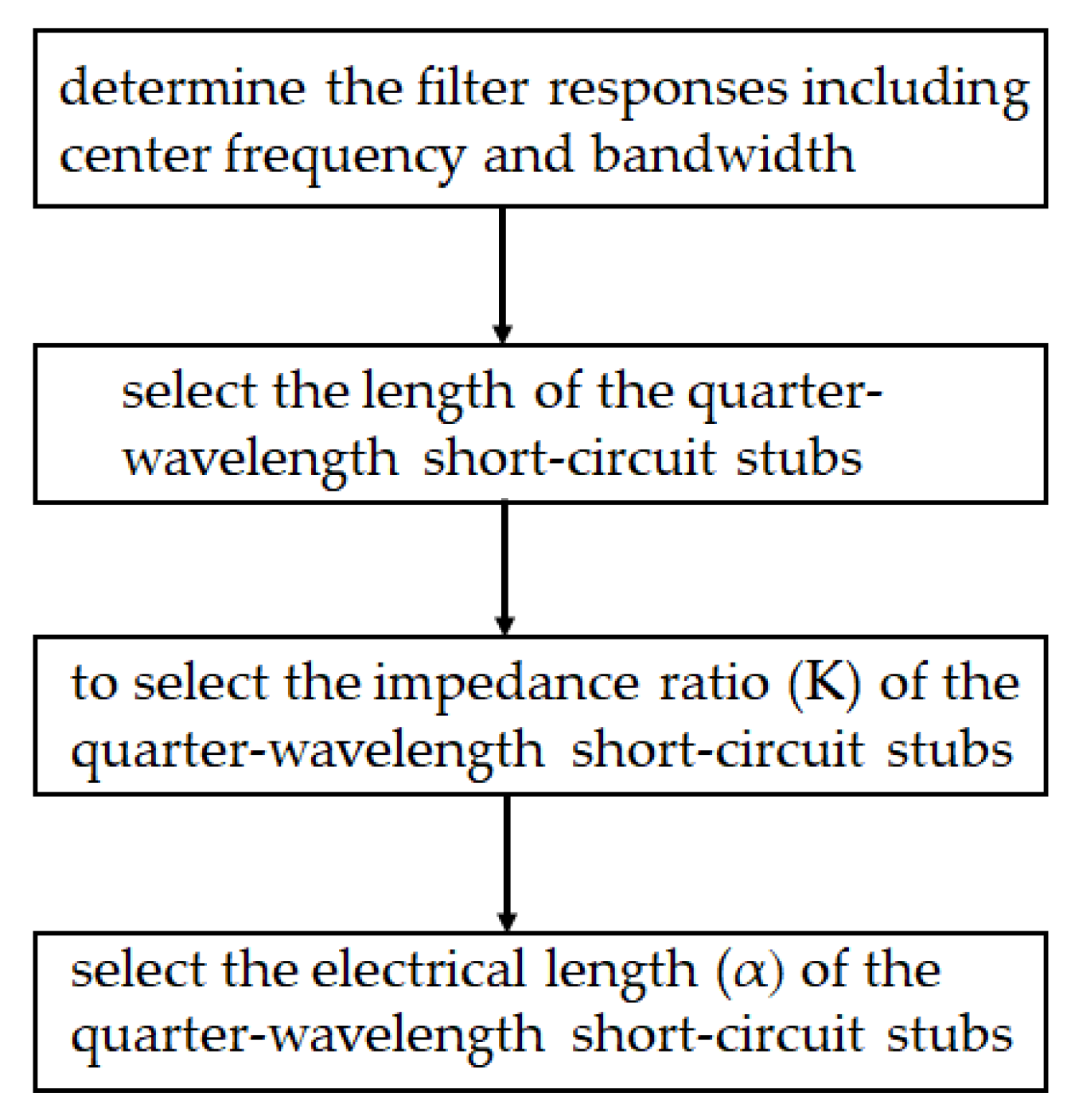
2. Design and Simulation

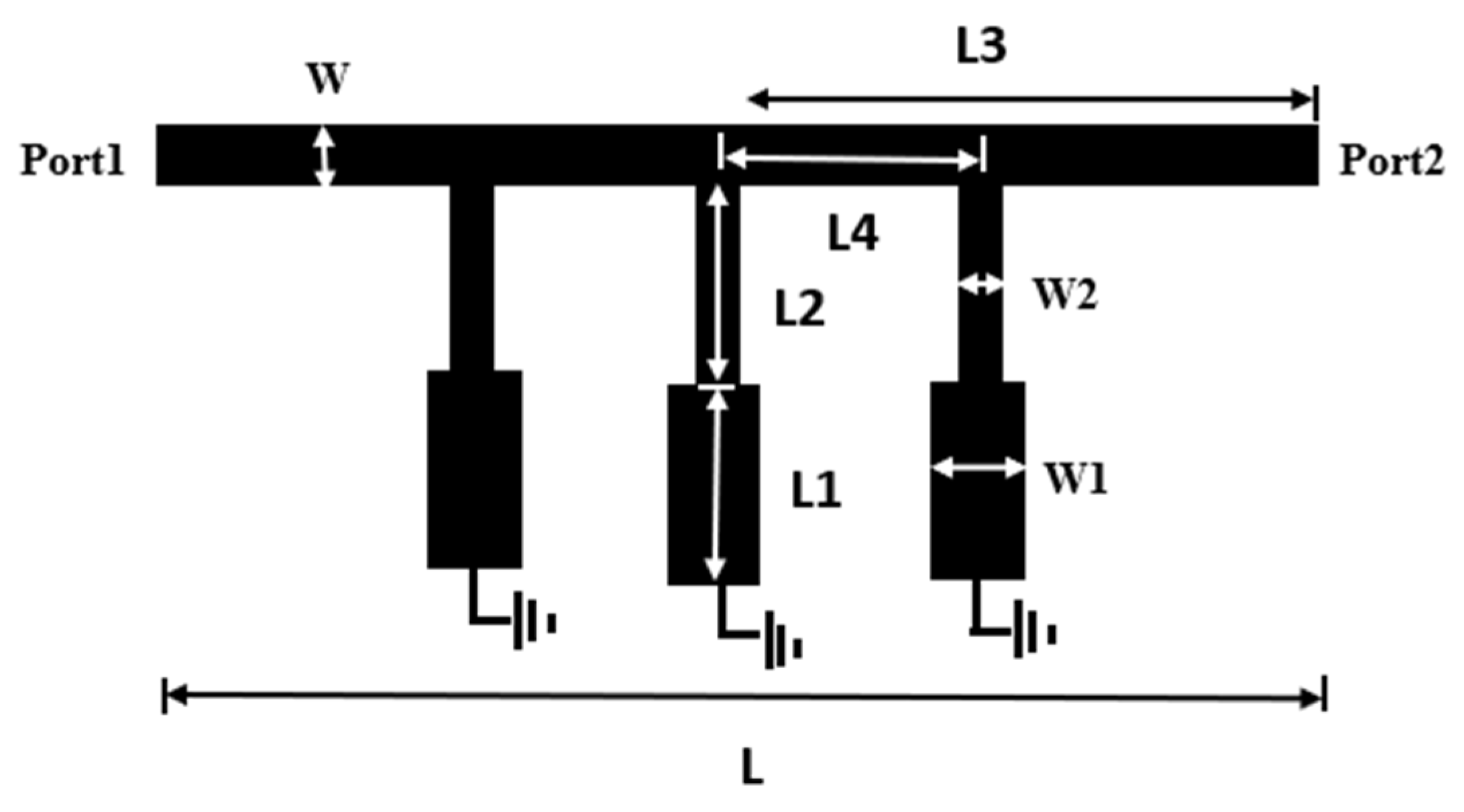
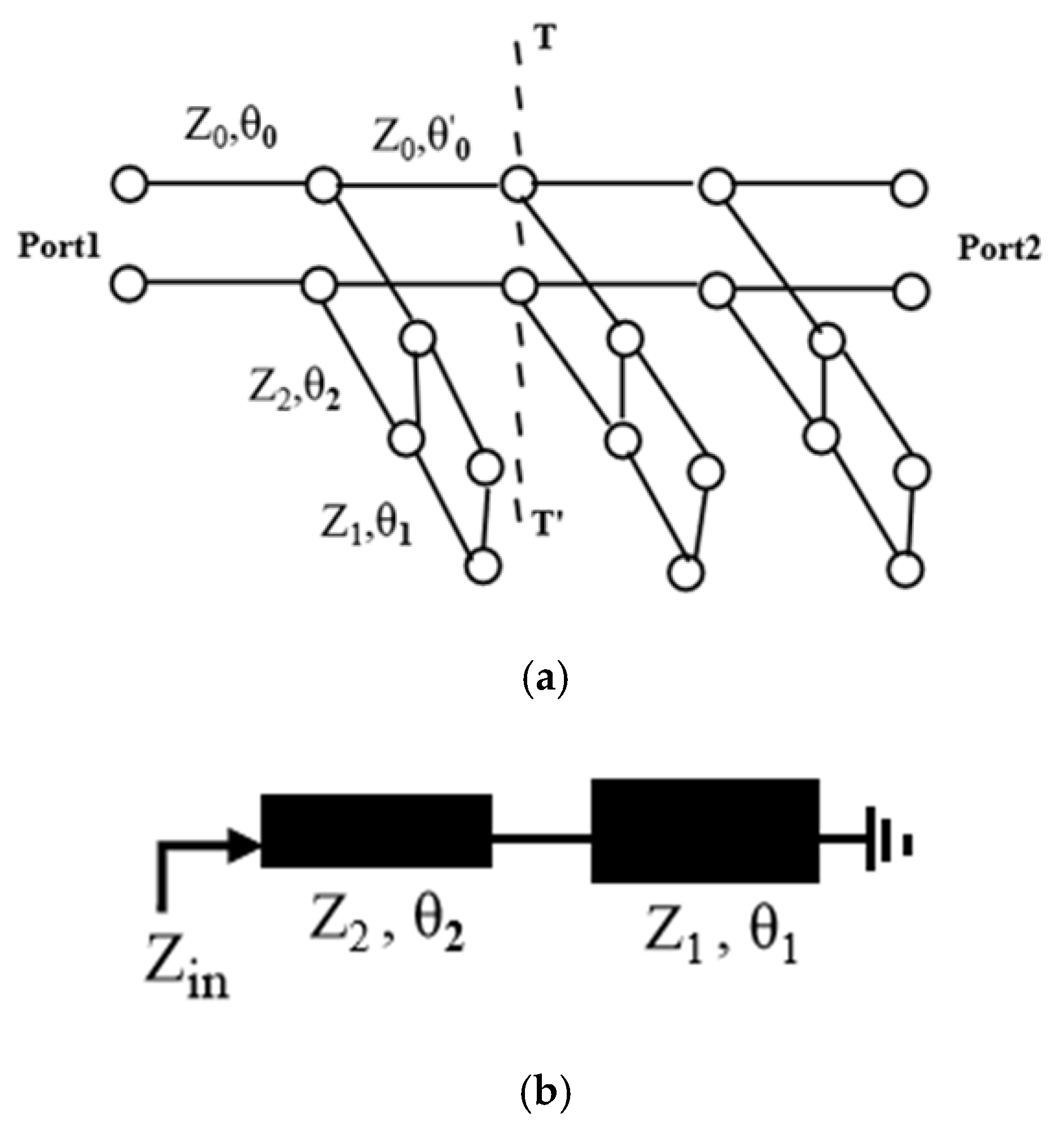
2.1. Equivalent Circuit

To analyze the resonance characteristics, an equivalent circuit model is presented. Figure 2 shows the equivalent circuit of the equivalent circuit of (a) the presented UWB BPF with a notched band for this design, and (b) the short-circuit step impedance stub. We used the equivalent structure of the traditional branch-loaded band stop filter, as discussed in [14]. It was assumed that the transmission line was lossless, ignoring the influence of the junction capacitance, the induction effect of the short-circuit stub, and the dispersion. Based on the transmission line network analysis, the formation of the presented design can be approximated. [R] is the transmission line model in Figure 2, which is obtained by multiplying the terminal line [U], the parallel short-circuit step impedance stub [V], and the connecting line [W]. The matrices [U] and [W] are still the same as in Equations (2) and (4); only the matrix [V] is replaced by the presented short-circuit step impedance stub. The overall matrix is ABCD, as shown in the following Equation (1):
[ R ] = [ A B C D ] = [ U ] [ V ] [ W ] [ V ] [ W ] [ V ] [ U ]
wherein
[ U ] = [ cos θ 0 j sin ( θ 0 ) Y 0 j Y 0 sin ( θ 0 ) cos θ 0 ]
[ V ] = [ 1 0 Y i 1 ]
[ W ] = [ cos ( θ 0 ) j sin ( θ 0 ) Y 0 j Y 0 sin ( θ 0 ) cos ( θ 0 ) ]
wherein Y0 is the admittance of the half-wavelength microstrip resonator and Yi in Equation (3) is the input admittance of the short-circuit step impedance stub, which is equal to the inverse of Zi, the input impedance of the short-circuit step impedance stub. Under the condition that the impedance is the matching source and load, the S parameter of the equivalent circuit is obtained by Equation (1):
S 11 = A + ( B / Z 0 ) C Z 0 D A + ( B / Z 0 ) + C Z 0 + D
S 21 = 2 A + ( B / Z 0 ) + Z 0 + D
The short-circuit step impedance stub is formed by an impedance unit (Z1) with an electrical length (θ1) and an impedance unit (Z2) with an electrical length (θ2). The impedance ratio is defined as K = Z1/Z2 and the electrical length ratio is defined as α = θ1/(θ1 + θ2) = θ1/θt [11]. The input impedance (Zin) of the short-circuit step impedance stub is derived as [1,11]:
Z i = j Z 2 Z 1 tan θ 1 + Z 2 tan θ 2 Z 2 Z 1 tan θ 1 tan θ 2
Figure 3 shows the flowchart to design the presented UWB BPF with a notched band using quarter-wavelength short-circuit step impedance stubs. The first step is to determine the filter responses including the center frequency and the required bandwidth; the second step is to select the length (L1 + L2) of the quarter-wavelength short-circuit stubs to match the center frequency; the third step is to select the impedance ratio (K) of sections L1 and L2 to control the bandwidth; and the fourth step is to select the electrical length (α) of sections L1 and L2 to shift the notched band. In this study, the required UWB response had a passband range of 2.5 GHz–10.5 GHz and a notched band around 5.1 GHz to suppress the WLAN band. The 0.8 mm thick FR4 substrate with a dielectric constant of 4.6 and a loss tangent of 0.00256 was used to design and manufacture the presented filter. During step 2 to step 4, the full wave electromagnetic software IE3D was used to match step 1 of this design [20]. Moreover, w = 1.52 mm, L3 = 18 mm, and L4 = 10 mm were fixed, and the used design parameters were the impedance ratio K and the electrical length ratio α.

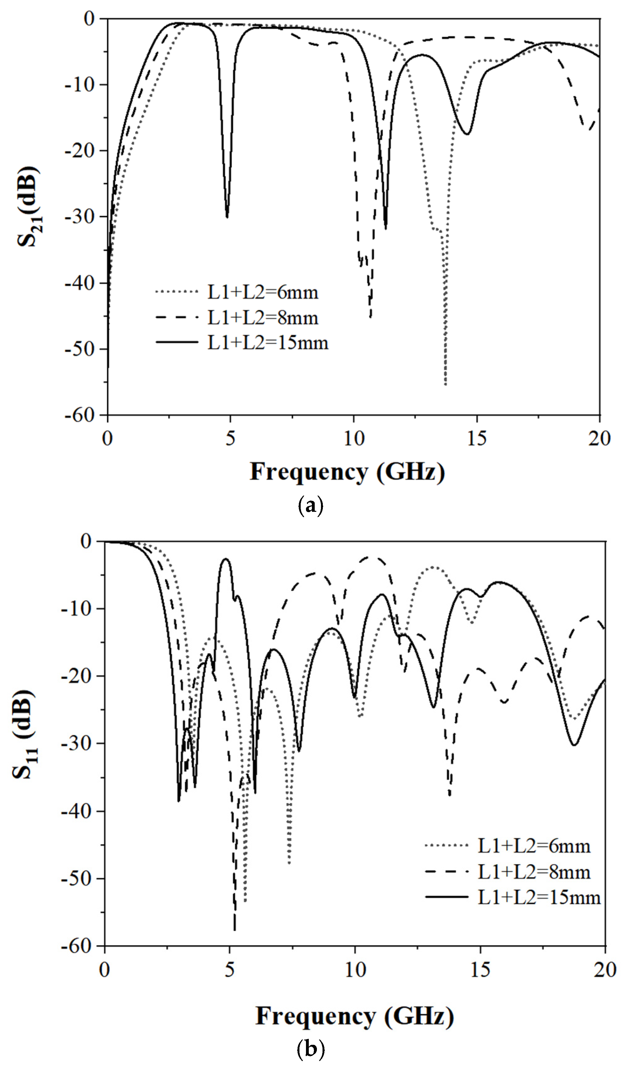
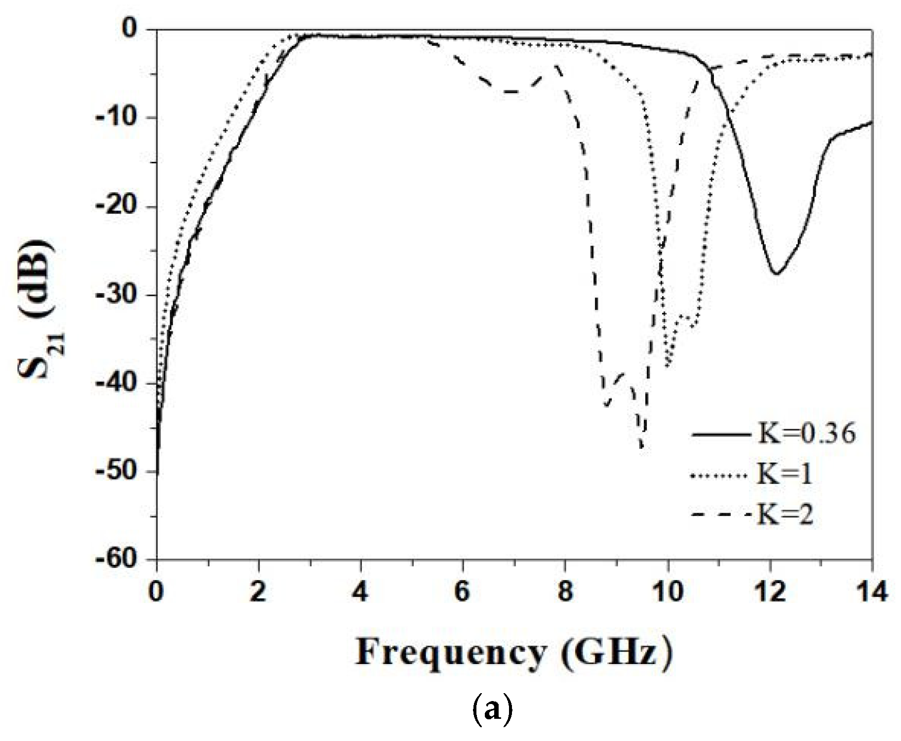
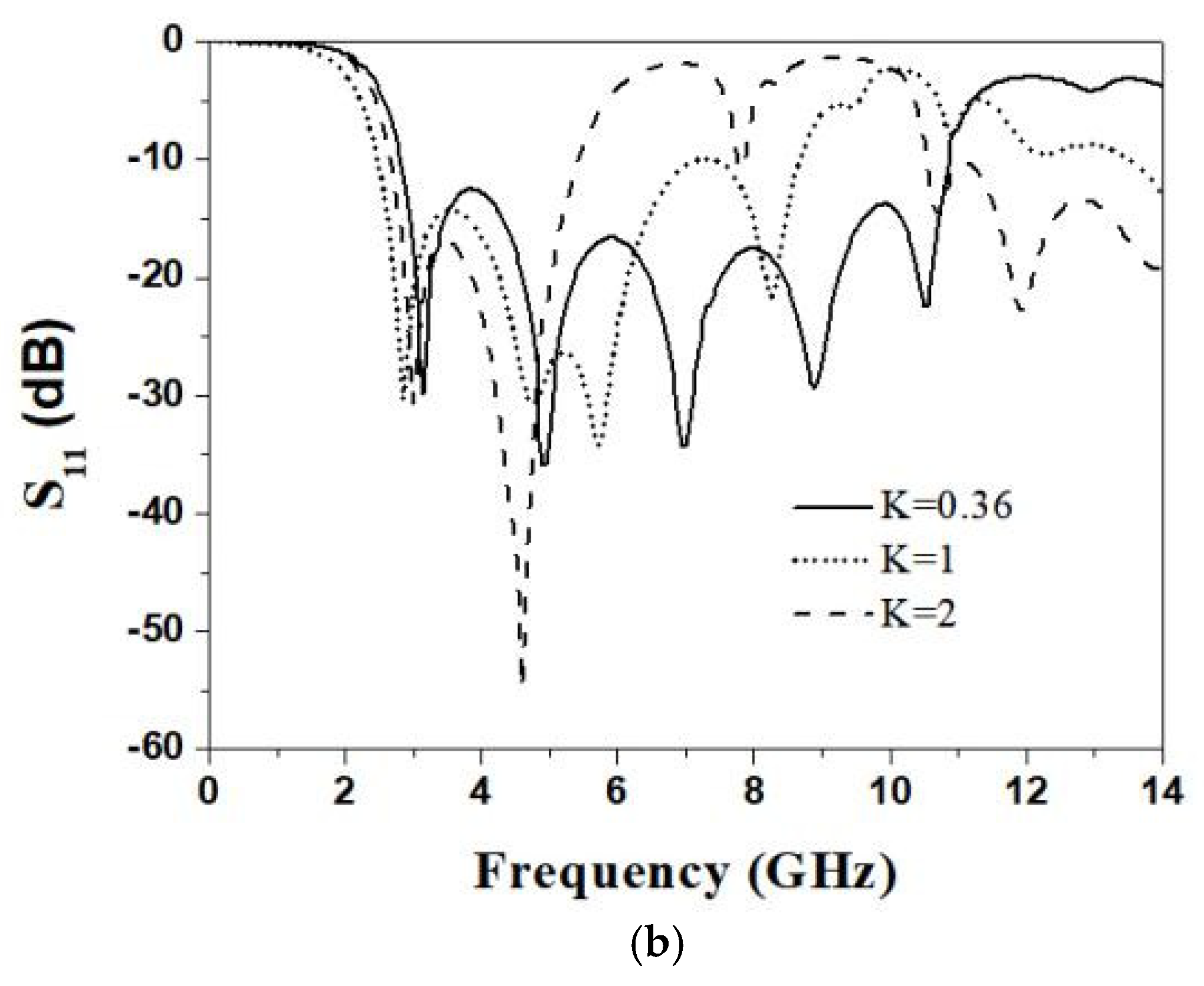
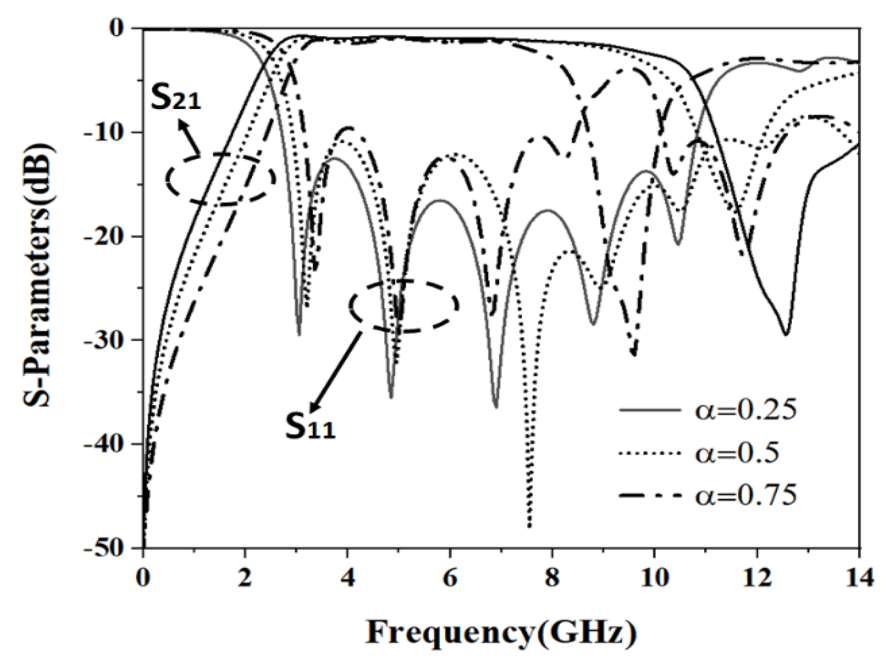
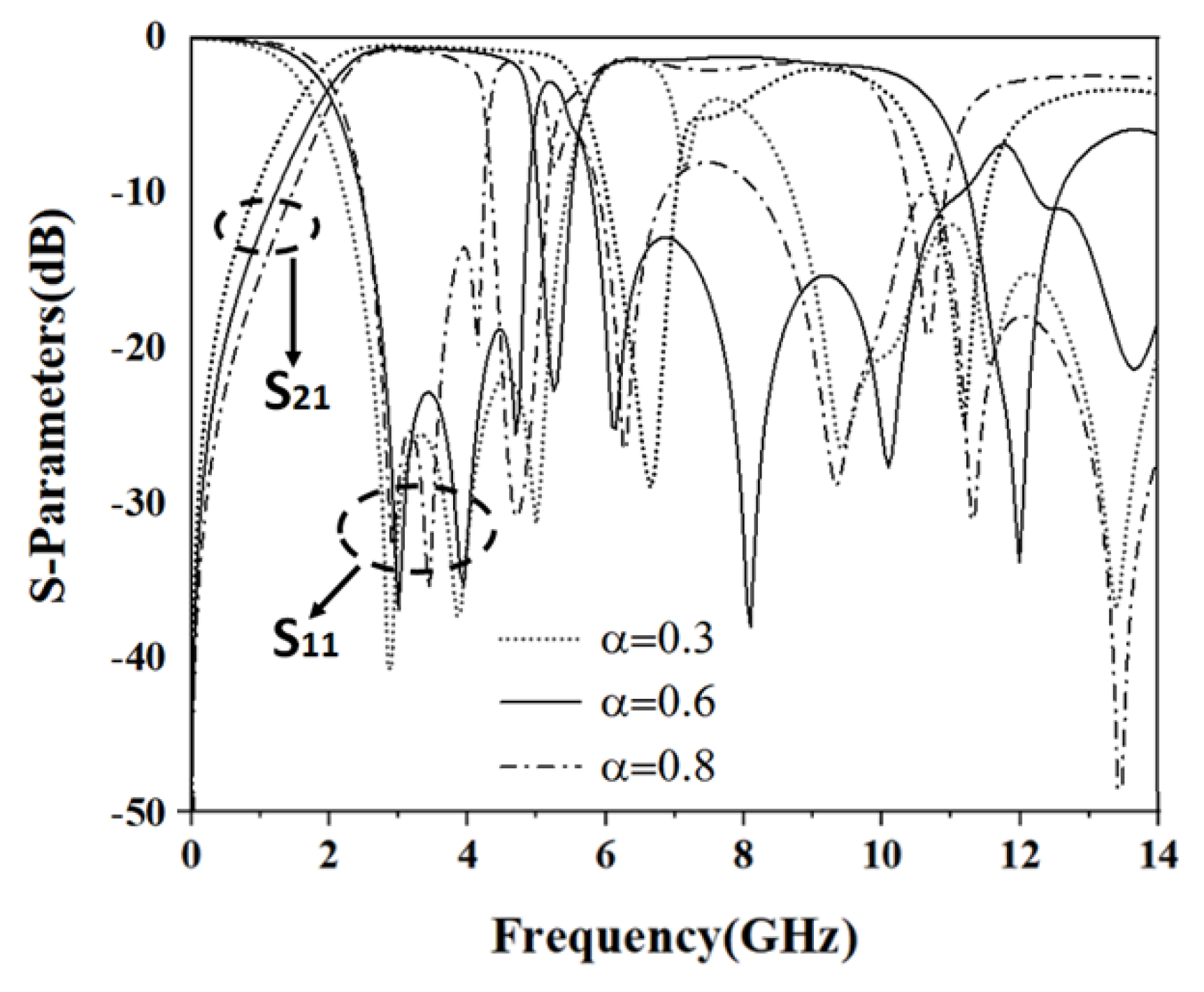
2.2. Parameter Analysis

Figure 4 shows the S-parameter variation diagram (a) S21 and (b) S11 under different lengths of the short-circuit step impedance stubs with K = 1. It is shown in Figure 3 that the positions of the first two notched bands are related to the length of the short-circuit step impedance stubs. The greater the length, the more the frequency of the notch moves toward the lower frequency. When L1 + L2 increases from 6 mm to 15 mm, the position of first notch changes from 14 GHz to 4.9 GHz. However, the lower passband side is still around 2 GHz; that is, the bandwidth of the wide passband would decrease as L1 + L2 increases.
Figure 5 shows the S parameter variation diagrams (a) S21 and (b) S11 under different impedance ratios K of quarter-wavelength short-circuit step impedance stubs with the electrical length ratio α of 0.25 and L1 + L2 = 18 mm. The other parameters in Figure 4 are shown in Table 1. As K is less than 1, the notched frequency moves to a higher frequency and thus the bandwidth of the wideband increases. Instead, when K is larger than 1, the notched frequency shifts to a lower frequency and thus the bandwidth of the wideband decreases.
Figure 6 shows the S parameter variation diagram under different electron length ratios α of quarter-wavelength short-circuit step impedance stubs with the impedance ratio K of 0.36 and L1 + L2 = 8 mm. It is shown that as the electron length ratios α become smaller, the first notched band moves to higher frequency and thus the bandwidth of the wideband increases.
Based on the above discussion, it is verified that by adjusting these design parameters, the frequencies of the notched band can be tuned widely, so a wide frequency band can be easily achieved. When K = 0.36 and α = 0.25, a UWB filter response is achieved with a center frequency of 6.65 GHz, a passband range of 2.5–10.8 GHz, a 3 dB fractional bandwidth (FBW) of 125%, an insertion loss of less than 1.26 dB, and a return loss larger than 10 dB on average. Moreover, it is expected that by choosing the impedance ratio (K) and electrical length ratio (α) appropriately, two wideband responses or a UWB response with a notched band could be obtained easily.

2.3. UWB BPF with a Notched Band

In order to effectively suppress the interference of wireless local area network (WLAN) signals, there is generally a notch at 5.15 GHz of the UWB BPF. Figure 7 shows the S-parameters of the designed filter under different electron length ratios α of quarter-wavelength short-circuit step impedance stubs with K = 0.36 and L1 + L2 = 15 mm. When the length ratio α increases, the position of the first two notched bands moves lower. By choosing L1 + L2 = 15 mm, K = 0.36, and α = 0.6, the position of the first two notched bands can meet the requirement for the UWB response with a notched band near 5.15 GHz.
Figure 8 is a simulated result of the designed UWB BPF with a notch band. The center frequency of the first UWB response was 3.5 GHz, and the passband range was 2.5 GHz–4.8 GHz. The center frequency of the second UWB response was 8.25 GHz, and the passband range was 5.8 GHz–10.5 GHz. The insertion loss in the entire passband was less than 1.26 dB, and the return loss was greater than 10 dB on average. Moreover, the notched band was at 5.15 GHz with a sharp attenuation that appeared on the left and right, and with an attenuation in the notch zone area of about 22.8 dB, which could effectively suppress the interference of the WLAN of the communication equipment.

3. Fabrication and Measurement

In order to verify the design theory, we manufactured and measured the designed filter. Its structure is shown in Figure 1. The actual production sizes were L = 36 mm, w = 1.52 mm, L1 = 9 mm, w1 = 3 mm, L2 = 6 mm, w2 = 0.5 mm, L3 = 18 mm, and L4 = 10 mm. Figure 9 shows (a) a physical image of the fabricated filter, (b) the simulated and measured frequency response results and (c) the group delay of the designed BPF. The overall circuit size was 36 mm × 31.52 mm, which was 0.285 λg × 0.095 λg, and λg was the waveguide wavelength of 4.9 GHz.
The network analyzer HP8722ES (Keysight Technologies, Santa Rosa, CA, USA) was used to test the frequency response of the fabricated filter. The measurement results show that the center frequency of the first UWB response was 3.5 GHz, the passband range was 2.4 GHz–4.8 GHz, the center frequency of the second UWB filter was 8.25 GHz, and the passband range was 5.8 GHz–10.5 GHz. The notched band was at 5.1 GHz with a sharp attenuation about 45 dB on the left and right. The insertion loss in the entire passband was less than 1.26 dB, and the return loss was larger than 10 dB on average. It is shown that the solder sizes were large in the fabricated sample; thus, this might cause some conductor loss and then degrade the measurement in the insertion loss in the entire passband. The maximum group delay change in the two passbands was less than 0.5 nS. The measured data had slightly drifted from the frequency of the simulation result. The main reason is that the needle used by the engraving machine was relatively thick, which caused the manufacturing error.
Table 2 shows the comparison of the filter performances of the presented filter with the previous works. Although there are many ways to design ultra-wideband characteristics [3,4,5,6,7,8,9,10,11,12,13,14,15,16,17,18,19], we only compared similar structures in Table 2. Namely, similar structures with the traditional lowpass filter with a uniform 50 Ω transmission line loaded with multiple quarter-wavelength short/open-circuit stubs were compared [15,16,17,18,19]. It is clearly shown that the presented design is different from the others and the performances are comparable to the other design. The benefit of the presented design is that it is easy to tune the wideband response and the notch band. The presented simple way to design a UWB filter in this article can not only achieve a relatively wide 3 dB bandwidth, but it can also achieve a notched band at 5.1 GHz, which can effectively suppress the effect of WLAN signals. However, the size of the designed filter is still large and could be further reduced by adopting the method shown in [4] which uses the folded structure combing with the SLR and the SIR, and the method presented in [13] which uses a series LC circuit, a miniaturizing inductor, and two transmission lines.

4. Conclusions

This paper has presented a simple way to design a UWB BPF with a notched band. The filter is composed of a half-wavelength microstrip resonator loaded with three sets of short-circuit step impedance stubs. Compared to the traditional quarter-wavelength uniform impedance stubs, the short-circuit step impedance stub provides two design parameters: the impedance ratio and the electrical length ratio. The advantage of this structure is that it is very easy to tune the frequencies of the first two notched bands widely by adjusting the impedance ratio (K) and the electrical length ratio (α); therefore, it is also easy to achieve a wide frequency band with a notched band. When the impedance ratio = 0.36 and the electrical length ratio = 0.6 of the short-circuit step impedance stubs, the overall filter response is composed of two UWB responses and a notched band. The measurement results show that the first UWB response had a passband range from 2.4 GHz to 4.6 GHz, and the second UWB response had a passband range from 5.6 GHz to 10.6 GHz. The insertion loss in the entire pass band was less than 1.26 dB, and the return loss was greater than 10 dB on average. The notched band with an attenuation of about 45 dB at 5.1 GHz had a sharp attenuation that appeared on the left and right. The maximum group delay change in the two passbands was less than 0.3 nS. Although the filter frequency drifted a little due to the manufacturing error, the designed filter still met the UWB requirements and had a high selectivity in the band. The presented structure has the advantage of a simple structure and an easy design.

Author Contributions

Conceptualization, M.-H.W.; Methodology, L.-Q.L. and H.-M.H.; Software, L.-Q.L.; Validation, L.-Q.L. and H.-M.H.; Formal Analysis, L.-Q.L. and H.-S.L.; Investigation, J.-J.C. and M.-H.W.; Resources, R.-Y.Y.; Data Curation, L.-Q.L. and J.-J.C.; Writing—Original Draft Preparation, H.-M.H. and M.-H.W.; Writing—Review and Editing, L.-Q.L. and R.-Y.Y.; Visualization, L.-Q.L. and M.-H.W.; Supervision, R.-Y.Y.; Project Administration, R.-Y.Y.; Funding Acquisition, M.-H.W. All authors have read and agreed to the published version of the manuscript.

Funding

This study was supported by the Natural Science Foundation of Fujian Province, China, fund number: 2020J01921.

Acknowledgments

The authors acknowledge Shih-Kun Liu for the help with the sample measurements.

Conflicts of Interest

The authors declare no conflict of interest.

References

  1. Hong, J.S. Microstrip Filters for RF/Microwave Applications, 2nd ed.; Wiley: New York, NY, USA, 2011. [Google Scholar]
  2. Revision of Part 15 of the Commission’s Rules Regarding Ultra-Wideband Transmission Systems; Federal Communication Commission: Washington, DC, USA, 2002.
  3. Chang, Y.-C.; Kao, C.-H.; Weng, M.-H.; Yang, R.-Y. Design of the Compact Wideband Bandpass Filter with Low Loss, High Selectivity and Wide Stopband. IEEE Microw. Wirel. Components Lett. 2008, 18, 770–772. [Google Scholar] [CrossRef]
  4. Yoon, K.; Kim, K. Design of Dual Ultra–Wideband Band–Pass Filter Using Stepped Impedance Resonator λg/4 Short Stubs and T–Shaped Band-Stop Filter. Electronics 2021, 10, 1951. [Google Scholar] [CrossRef]
  5. Fan, J.; Zhan, D.; Jin, C.; Luo, J. Wideband Microstrip Bandpass Filter Based on Quadruple Mode Ring Resonator. IEEE Microw. Wirel. Components Lett. 2012, 22, 348–350. [Google Scholar] [CrossRef]
  6. Yang, L.; Choi, W.W.; Tam, K.W.; Zhu, L. Novel wideband bandpass filter with dual notched bands using stub-loaded resonators. IEEE Microw. Wirel. Compon. Lett. 2017, 27, 25–27. [Google Scholar] [CrossRef]
  7. Feng, G.-X.; Wen, J.; Che, W.-Q. Compact Ultra-wideband bandpass filter with improved upper stopband using open/shorted stubs. IEEE Microw. Compon. Lett. 2017, 17, 123–125. [Google Scholar]
  8. Jankovi, N.; Niarchos, G.; Crnojević-Bengin, V. Compact UWB bandpass filter based on grounded square patch resonator. Electron. Lett. 2016, 52, 372–774. [Google Scholar] [CrossRef]
  9. Liu, J.; Ding, W.; Chen, J.; Zhang, A. New Ultra-Wideband Filter with Sharp Notched Band Using Defected Ground Structure. Prog. Electromagn. Res. Lett. 2019, 83, 99–105. [Google Scholar] [CrossRef] [Green Version]
  10. Ji, X.-C.; Ji, W.-S.; Feng, L.-Y.; Tong, Y.-Y.; Zhang, Z.-Y. Design of a Novel Multi-Layer Wideband Bandpass Filter with a Notched Band. Prog. Electromagn. Res. Lett. 2019, 82, 9–16. [Google Scholar] [CrossRef] [Green Version]
  11. Zhou, C.-X.; Guo, P.-P.; Zhou, K.; Wu, W. Design of a compact UWB filter with high selectivity and super wide stopband. IEEE Microw. Wirel. Compon. Lett. 2017, 27, 636–638. [Google Scholar] [CrossRef]
  12. Liu, J.; Zhang, Y.-H.; Wan, X.; Jing, H.-S. Miniaturized dual-mode ultra-wideband filter using sector substrate integrated waveguide. Microw. Opt. Technol. Lett. 2021, 63, 2343–2347. [Google Scholar] [CrossRef]
  13. Jamshidi, M.-B.; Roshani, S.; Talla, J.; Roshani, S.; Peroutka, Z. Size reduction and performance improvement of a microstrip Wilkinson power divider using a hybrid design technique. Sci. Rep. 2021, 11, 7773. [Google Scholar] [CrossRef]
  14. Roshani, S.; Jamshidi, M.B.; Mohebi, F.; Roshani, S. Design and Modeling of a Compact Power Divider with Squared Resonators Using Artificial Intelligence. Wirel. Pers. Commun. 2021, 117, 2085–2096. [Google Scholar] [CrossRef]
  15. Pozar, D.-M. Microwave Engineering, 2nd ed.; Wiley: New York, NY, USA, 1998. [Google Scholar]
  16. Raman, S.; Soni, A. UWB bandpass filter with quarter wavelength short circuited stubs. Int. J. Sci. Eng. Res. 2013, 4, 1345–1348. [Google Scholar]
  17. Uikey, R.; Sangam, R.-S.; Prasadu, K.; Rakhesh, S.-K. Novel notched UWB filter using stepped impedance stub loaded microstrip resonator and spurlines. Int. J. Microw. Sci. Tech. 2015, 2015, 939521. [Google Scholar] [CrossRef]
  18. Parvez, S.; Sakib, N.; Mollah, M.-N. Chebyshev quarter wavelength wideband bandstop filter based on dumbbell annular ring resonator. In Proceedings of the IEEE International Conference on Electrical Computer and Communication Engineering (ECCE), Cox’s Bazar, Bangladesh, 16–18 February 2017; pp. 891–894. [Google Scholar]
  19. Sangam, R.-S.; Kshetrimayum, R.-S. Notched UWB filter using exponential tapered impedance line stub loaded microstrip resonator. J. Eng. 2018, 9, 768–772. [Google Scholar] [CrossRef]
  20. IE3D Simulator; Zeland Software. Available online: www.zeland.com (accessed on 10 September 2004).
Figure 1. The structure of the designed UWB BPF with a notched band.
Electronics 11 01124 g001
Figure 2. The equivalent circuit of (a) the presented UWB BPF with a notched band for this design, and (b) the quarter-wavelength short-circuit step impedance stub.
Electronics 11 01124 g002
Figure 3. The flowchart to design the presented UWB BPF with a notched band using quarter-wavelength short-circuit step impedance stubs.
Electronics 11 01124 g003
Figure 4. S-parameter variation diagram under different lengths of quarter-wavelength short-circuit step impedance stubs with K = 1 (a) S21 and (b) S11. (L = 36 mm, w = 1.52 mm, w1 = w2 = 0.5 mm, L3 = 18 mm, L4 = 10 mm).
Electronics 11 01124 g004
Figure 5. S parameter variation diagrams (a) S21 and (b) S11 under different impedance ratios K of quarter-wavelength short-circuit step impedance stubs with the electrical length ratio α of 0.25 and L1 + L2 = 8 mm. (L = 36 mm, w = 1.52 mm, L3 = 18 mm, L4 = 12 mm).
Electronics 11 01124 g005aElectronics 11 01124 g005b
Figure 6. S parameter variation diagram under different electronic length ratios α of quarter-wavelength short-circuit step impedance stubs with the impedance ratio K of 0.36 and L1 + L2 = 8 mm. (L = 36 mm, w = 1.52 mm, L3 = 18 mm, L4 = 12 mm, w1 = 3 mm, w2 = 0.5 mm).
Electronics 11 01124 g006
Figure 7. S-parameters of the designed filter under different electron length ratios α of quarter-wavelength short-circuit step impedance stubs with K = 0.36 and L1 + L2 = 15 mm. (w1 = 3 mm, w2 = 0.5 mm, L = 36 mm, w = 1.52 mm, L3 = 18 mm, L4 = 10 mm).
Electronics 11 01124 g007
Figure 8. Simulated result of the designed UWB BPF with a notch band with K = 0.36, α = 0.6, w1 = 3 mm, w2 = 0.5 mm, L2 = 6 mm, L1 = 9 mm, L = 36 mm, w = 1.52 mm, L3 = 18 mm, L4 = 10 mm.
Electronics 11 01124 g008
Figure 9. (a) Physical image of the fabricated filter, (b) the simulated and measured frequency response results, and (c) the group delay of the designed BPF.
Electronics 11 01124 g009
Table 1. Parameters in Figure 4.
Impedance Ratio KLine Width of the High Impedance LineCharacteristic Impedance of the High Impedance LineLine Width of the High Impedance LineCharacteristic Impedance of the High Impedance Line
0.36w1 = 0.5 mm87 Ωw2 = 3 mm32 Ω
1w1 = 0.5 mm87 Ωw2 = 0.5 mm87 Ω
2w1 = 0.5 mm87 Ωw2 = 0.04 mm174 Ω
Table 2. Comparison of filter performances of the presented filter with previously published works.
Filter Performances Ref. [15]Ref. [16]Ref. [17]Ref. [18]Ref. [19]This Work
Stub typeopenshortopenopenshortshort
Center frequency (GHz)4.07.237.2526.856.65
3 dB FBW (%)Low pass106112113121125
Circuit Size (λg × λg)-1.36 × 0.33-0.97 × 0.27-0.285 × 0.095
Group delay (ns)-0.26<0.70.45<0.350.3
notchNoNoYesNoYesYes
Notch-band rejection level, dB--39-3245
Notch band FBW, %--15.6-95
Notch frequency, GHz--5.9-~5.55.1
Extra structurenonoDefect groundspurlinenono
Publisher’s Note: MDPI stays neutral with regard to jurisdictional claims in published maps and institutional affiliations.

