Novel Approach and Methods for Optimizing Highly Sensitive Low Noise Amplifier CMOS IC Design for Congested RF Environments
Abstract
:1. Introduction
2. Design Topology and Strategies
2.1. Circuit Topology
2.2. Parameters Determination Strategy
- Step 1. Set the power budget by setting current through the cascode amplifier.
- Step 2. Determine the channel length.
- Step 3. Vary and find corresponding points.
- Step 4. Get for the points from step 3.
- Step 5. Compute width for the values in step 4.
- Step 6. Run simulations on gain, noise figure, and linearity.
- Step 7. Evaluate the FoM and finalize parameters.
3. Simulation Results and Parameter Set-Up
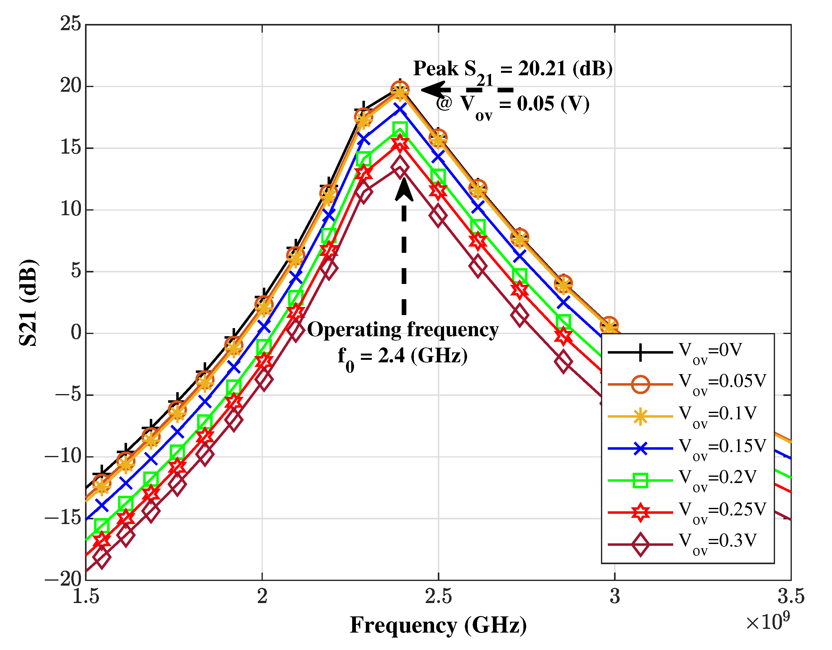
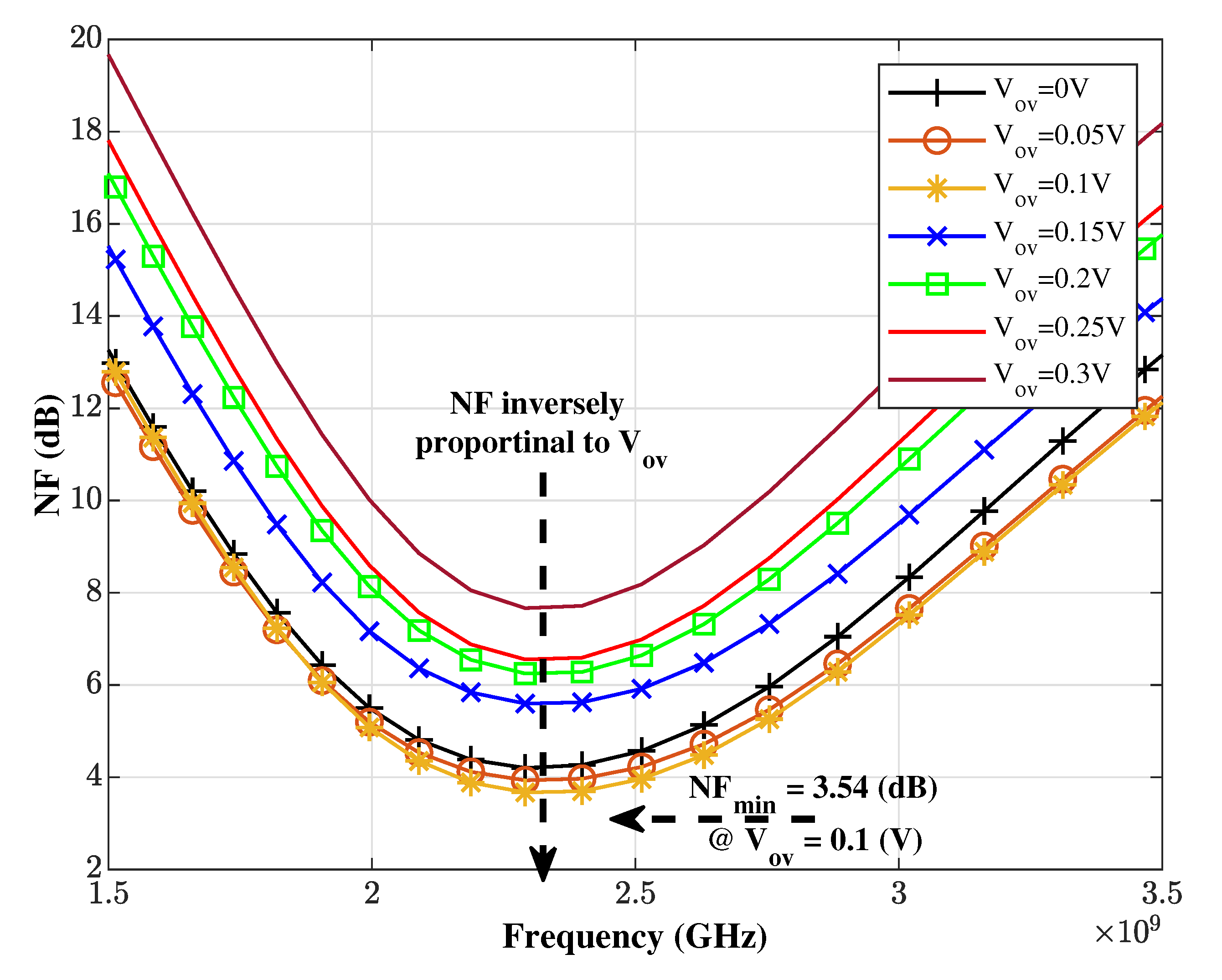
3.1. Simulation for Each
3.2. Optimized Parameters and Reliability Simulations
- (typical-typical), , 27 °C
- (slow-slow), 0.9, −23 °C
- (fast-fast), , 127 °C
4. Conclusions
Author Contributions
Funding
Data Availability Statement
Conflicts of Interest
References
- Iliadis, A.; Kim, K. Theoretical foundation for upsets in CMOS circuits due to high-power electromagnetic interference. IEEE Trans. Device Mater. Reliab. 2010, 10, 347–352. [Google Scholar] [CrossRef]
- Pinjare, S.; Nithya, G.; Nagaraja, V.; Sthuthi, A. A Gm/Id Based Methodology for Designing Common Source Amplifier. In Proceedings of the 2018 2nd International Conference on Micro-Electronics and Telecommunication Engineering (ICMETE), Ghaziabad, India, 20–21 September 2018. [Google Scholar]
- Chung, J.; Iliadis, A. Modeling a High Linearity, Low Noise Gilbert Cell Mixer using Three Optimization Techniques. In Proceedings of the 2020 IEEE 63rd International Midwest Symposium On Circuits And Systems (MWSCAS), Springfield, MA, USA, 9–12 August 2020; pp. 790–793. [Google Scholar]
- Balodi, D.; Verma, A.; Govidacharyulu, P. A high gain low noise amplifier design & comparative analysis with other MOS-topologies for Bluetooth applications at 130nm CMOS. In Proceedings of the 2016 IEEE Industrial Electronics and Applications Conference (IEACon), Kota Kinabalu, Malaysia, 20–22 November 2016; pp. 378–383. [Google Scholar]
- Chung, J.; Iliadis, A. Design and optimization of a CMOS IC novel RF tracking sensor. Int. J. Circuit Theory Appl. 2021, 49, 801–819. [Google Scholar] [CrossRef]
- Arshad, S.; Ramzan, R.; Qamar-ul-Wahab. Wideband common gate LNA with novel input matching technique. In Proceedings of the 2016 5th International Conference on Modern Circuits and Systems Technologies (MOCAST), Thessaloniki, Greece, 12–14 May 2016. [Google Scholar]
- Shim, Y.; Kim, C.; Lee, J.; Lee, S. Design of full band UWB common-gate LNA. IEEE Microw. Wirel. Compon. Lett. 2007, 17, 721–723. [Google Scholar] [CrossRef]
- Eshghabadi, F.; Banitorfian, F.; Noh, N.; Mustaffa, M.; Abd Manaf, A. Fully-hybrid computer-aided RF LNA design and evaluation for GSM-1900 standard band. In Proceedings of the 2015 6th Asia Symposium On Quality Electronic Design (ASQED), Kula Lumpur, Malaysia, 4–5 August 2015; pp. 177–180. [Google Scholar]
- Chen, Y.-C.; Kuo, C.-N. A 6-10-GHz ultra-wideband tunable LNA. Proc. IEEE Int. Symp. Circuits Syst. 2005, 5, 5099–5102. [Google Scholar]
- Lin, Y.; Wang, C.; Lee, G.; Chen, C. High-Performance Wideband Low-Noise Amplifier Using Enhanced π-Match Input Network. IEEE Microw. Wirel. Components Lett. 2014, 24, 200–202. [Google Scholar] [CrossRef]
- Jussila, J.; Sivonen, P. A 1.2-V Highly Linear Balanced Noise-Cancelling LNA in 0.13-μm CMOS. IEEE J. Solid-State Circuits 2008, 43, 579–587. [Google Scholar] [CrossRef]
- Li, X. Low Noise Design Techniques for Radio Frequency Integrated Circuits. Bachelor’s Thesis, University of Washington, Seattle, WA, USA, 2004. [Google Scholar]
- Aneja, A.; Li, X.; Chong, P. Design and analysis of a 1.1 and 2.4 GHz concurrent dual-band low noise amplifier for multiband radios. AEU Int. J. Electron. Commun. 2021, 134, 153654. [Google Scholar] [CrossRef]
- Park, B.; Kwon, K. 2.4-GHz Bluetooth low energy receiver employing new quadrature low-noise amplifier for low-power low-voltage IoT applications. IEEE Trans. Microw. Theory Tech. 2021, 69, 1887–1895. [Google Scholar] [CrossRef]
- Luo, Y.; Xia, T. Design of Reconfigurable Low Noise Amplifier Based on Active Inductor. In Proceedings of the 2020 IEEE International Conference on Artificial Intelligence and Computer Applications (ICAICA), Dalian, China, 27–29 June 2020. [Google Scholar]
- Liu, Z.; Boon, C.; Yu, X.; Li, C.; Yang, K.; Liang, Y. A 0.061-mm2 1–11-GHz Noise-Canceling Low-Noise Amplifier Employing Active Feedforward With Simultaneous Current and Noise Reduction. IEEE Trans. Microw. Theory Tech.. 2021, 69, 3093–3106. [Google Scholar] [CrossRef]
- Bozorg, A.; Staszewski, R. A 0.02–4.5-GHz LN(T)A in 28-nm CMOS for 5G exploiting noise reduction and current reuse. IEEE J. Solid-State Circuits 2021, 56, 404–415. [Google Scholar] [CrossRef]
- Chang, J.; Lin, Y. 3–9-GHz CMOS LNA using body floating and self-bias technique for sub-6-GHz 5G communications. IEEE Microw. Wirel. Components Lett. 2021, 31, 608–611. [Google Scholar] [CrossRef]
- Gao, H.; Li, N.; Li, M.; Wang, S.; Zhang, Z.; Kuan, Y.; Yu, X.; Gu, Q.; Xu, Z. A 6.5–12 GHz balanced variable gain low-noise amplifier with frequency-selective non-foster gain equalization technique. In Proceedings of the 2020 IEEE/MTT-S International Microwave Symposium (IMS), Los Angeles, CA, USA, 4–6 August 2020. [Google Scholar]


| (V) | (1/V) | (GHz) | (dB) | IIP3 (dBm) | NF (dB) | W (m) | FoM |
|---|---|---|---|---|---|---|---|
| 0 | 25.6 | 2.8 | 19.72 | 4.47 | 4.1 | 588 | 3.16 |
| 0.05 | 12.2 | 11 | 20.21 | 4.87 | 3.98 | 295 | 3.67 |
| 0.1 | 10 | 15.8 | 19.91 | 5.89 | 3.54 | 178 | 3.62 |
| 0.15 | 7.9 | 20 | 18.62 | 6.52 | 5.62 | 117 | 2.92 |
| 0.2 | 6.5 | 24.1 | 16.6 | 7.9 | 6.2 | 84 | 2.8 |
| 0.25 | 5.4 | 27 | 15.3 | 8.96 | 6.45 | 65 | 2.79 |
| 0.3 | 4.6 | 31 | 13.21 | 10.21 | 7.89 | 74 | 2.17 |
| Reference | (dB) | NF (dB) | IIP3 (dBm) | Power (mW) | (GHz) | Supply Voltage (V) | Area () | CMOS Tech (nm) |
|---|---|---|---|---|---|---|---|---|
| This work | 19.91 | 3.54 | 5.89 | 9 | 2.4 | 1.8 | 0.26 | 180 |
| Aneja [13] | 20.1 | 3 | 4.9 | 108 | 2.4 | 3 | N/A | MIC |
| Park [14] | 49.5 | 8.2 | −25.75 | 2.16 | 2.4 | 0.8 | 1.16 | 65 |
| Luo [15] | 19 | 2.65 | N/A | 20.1 | 2.4 | 1.8 | 0.023 | 180 |
| Liu [16] | 14–17 | 3.5–5.5 | −2.8 | 9 | 1–11 | 1.2 | 0.061 | 40 |
| Bozorg [17] | 15.2 | 2.09–3.2 | −4.6–3.5 | 4.5 | 0.02–4.5 | 1 | 0.03 | 28 |
| Chang [18] | 7.5–10.7 | 3.41 | −6.2 | 3.3 | 2.4–9.1 | 1 | 0.74 | 180 |
| Gao [19] | 20.7 | 3.26 | −12 | 75 | 6.5–12 | 1.3 | 0.98 | 55 |
Publisher’s Note: MDPI stays neutral with regard to jurisdictional claims in published maps and institutional affiliations. |
© 2022 by the authors. Licensee MDPI, Basel, Switzerland. This article is an open access article distributed under the terms and conditions of the Creative Commons Attribution (CC BY) license (https://creativecommons.org/licenses/by/4.0/).
Share and Cite
Chung, J.; Iliadis, A.A. Novel Approach and Methods for Optimizing Highly Sensitive Low Noise Amplifier CMOS IC Design for Congested RF Environments. Electronics 2022, 11, 976. https://doi.org/10.3390/electronics11070976
Chung J, Iliadis AA. Novel Approach and Methods for Optimizing Highly Sensitive Low Noise Amplifier CMOS IC Design for Congested RF Environments. Electronics. 2022; 11(7):976. https://doi.org/10.3390/electronics11070976
Chicago/Turabian StyleChung, Jooik, and Agis A. Iliadis. 2022. "Novel Approach and Methods for Optimizing Highly Sensitive Low Noise Amplifier CMOS IC Design for Congested RF Environments" Electronics 11, no. 7: 976. https://doi.org/10.3390/electronics11070976
APA StyleChung, J., & Iliadis, A. A. (2022). Novel Approach and Methods for Optimizing Highly Sensitive Low Noise Amplifier CMOS IC Design for Congested RF Environments. Electronics, 11(7), 976. https://doi.org/10.3390/electronics11070976


