Article

An Auto Adjustable Transimpedance Readout System for Wearable Healthcare Devices

1
Department of Electrical Engineering, University of Texas at Arlington, Arlington, TX 76019, USA
2
School of Electronic Engineering, Kumoh National Institute of Technology, Gumi 39177, Korea
*
Authors to whom correspondence should be addressed.
Electronics 2022, 11(8), 1181; https://doi.org/10.3390/electronics11081181
Submission received: 7 March 2022 / Revised: 28 March 2022 / Accepted: 5 April 2022 / Published: 8 April 2022
(This article belongs to the Section Circuit and Signal Processing)

Abstract

:
The objective of this work was to design a versatile readout circuit for patch-type wearable devices consisting of a Transimpedance Amplifier (TIA). The TIA performs Current to Voltage (I–V) conversion, the most widely used technique for amperometry and impedance measurement for various types of electrochemical sensors. The proposed readout circuit employs a digitally controllable feedback resistor ( R f ) technique in the TIA to improve accuracy, which can be utilized in a variety of electrochemical sensors within a current range of 0.1 µA–100 µA. It is designed to accommodate multiple sensors simultaneously to track multiple target analytes for high accuracy and versatile usage. The readout circuit consists of low power operational amplifier (op–amp) and digital circuit blocks, is designed and fabricated with Magna 0.18 µm Complementary Metal Oxide Semiconductor (CMOS) technology, which provides low power consumption and a high degree of integration. The design has a small size of 0.282 mm 2 and low power consumption of 0.38 mW with a 3.3 V power supply, which are desirable factors in wearable device applications.

1. Introduction

Wearable devices have emerged as powerful tools for environmental examination, healthcare devices, and motion recognition, despite some challenges such as miniaturization and low power while ensuring accuracy, that limit their widespread applicability as continuous monitoring systems of target information [1,2,3]. Especially with the current trend in an acceleration of global population aging, one-third of the population has been reported to be over 60 years of age in most regions by 2050, resulting in a high demand for healthcare wearable devices [4]. Since the immune response declines with age, the elderly might suffer from many more health risks, which requires healthcare workforces [5]. The wearable devices could be used to address some of the challenges related to detecting and managing adverse health conditions in aging populations, and to reducing ubiquitous healthcare issues [6,7]. As the demand for wearable devices for healthcare continues to rise, it has generated a booming market, and the companies are now seeing the opportunities of supplying wearable healthcare technologies to their consumers as beneficial. So far, wristwatches, gloves, patches, headbands, eyeglasses, and necklaces have been reported as types of wearable devices [8,9,10,11,12,13,14,15,16]. The wristwatch is the most affordable and widely invented wearable device type since it can provide good wearing comfort and obtain information from the skin. At the same time, it does not require flexibility other than the wristband part, which indicates that commercial-off-the-shelf (COTS) can be utilized as components to build readout circuits for interpreting sensors’ information. As a result, we can find watch type of commercial products easily available in the market, such as the Apple Watch (Apple Inc., Cupertino, CA, USA), Fitbit (Fitbit, San Francisco, CA, USA), Samsung Galaxy Watch (Samsung Electronics, Suwon, Korea), and so on. Those mentioned commercial products show positive effects to improve people’s life quality and reduce the potential emergency situation; however, they have limitations as healthcare devices since they are mainly focused on motion recognition utilizing accelerometer and gyroscope to track physical activities, not electrochemical sensors or biosensors which can diagnose or sense symptoms of disease from the body. The mentioned limitation makes them not suitable for accurate and multifunctional healthcare devices. For example, in the case of stress, which is considered a source of many types of illness, a watch type stress monitoring device is not able to perform a comprehensive stress analysis since it can only measure skin conductance [15].
Recent research studies in the sensor field have explored various wearable sensors for monitoring electrophysiological signals and bio-analytes [17,18,19,20,21]. Epidermal materials provide classes of skin-mounted sensors in physical formats that enable intimate, conformal contact with the skin. The soft, non-irritating nature of this contact yields an interface that simultaneously provides high precision and high accuracy measurement of biophysiological parameters, such as temperature, hydration, strain, and biopotential. Such epidermal sensors are ultrathin, breathable, and stretchable, with mechanical and thermal properties that closely match to the skin itself to enable effective skin integration with minimum constraints on natural processes [18,19]. Not limited to developing single target wearable flexible sensors, the latest studies are trying to adopt multifunctional sensors in a single platform [17,18,20,21]. For instance, one research group reported a multifunctional sweat-based electrochemical physiological hybrid skin patch for precise glucose detection in sweat with pH and temperature correction and simultaneous monitoring of electrocardiogram (ECG) [20]. However, only a few of the complete patch type devices have been reported due to the constraints on readout circuits. The readout circuits can be implemented using COTS or Integrated Circuit (IC). Generally, the COTS is preferred in most of the readout circuits for wearable devices since it is easily accessible, so that less time is required to prove the concept. However, readout circuit comprised of COTS is not suitable as patch type of the device since it is not flexible nor miniaturized. Especially, if the readout circuit needs to deal with multiple sensors, the burden increases because it requires more COTS components. Therefore, to avoid utilizing COTS components, devices consist of a sensor and a Radiofrequency (RF) antenna, where sensor output is voltage since an RF antenna can only transfer voltage information [22]. In other works, if patch type of the healthcare device’s sensor output is a current, only sensor validation is conducted with test equipment through external wires [17,21]. Therefore, the I–V converter designed in IC for multiple sensors is required to build a complete patch type of the healthcare device. Moreover, the IC is not only offering miniaturization but also shows better accuracy than the COTS.
Herein, we report a versatile and wide ranged I–V converter circuit for multiple patch type of sensors which is fabricated using the Complementary Metal Oxide Semiconductor (CMOS) process. It can accommodate five sensors, which can be expandable; its measurable sensor current range is 0.1 μ A to 100 μ A, which is chosen based on the practical sensor output current range [23,24,25]. The rest of this paper is organized as follows. Section 2 describes the specifications and design of the proposed readout circuit. Then, Section 3 discusses simulation and IC test results. Finally, the conclusion is drawn in Section 4.

2. Design of Readout Circuit

Several high-performance current measurement circuit topologies are discussed in [26,27,28,29,30,31,32,33,34,35,36,37,38,39,40,41]. One of the common architectures for low current measurements is based on an integrator followed by a differentiator [34,35,36]. This structure provides a high gain and linear response at the cost of a low dynamic range of about 5 decades and takes a long time to accumulate the small current into a measurable voltage signal. Moreover, the integrator is prone to saturation and requires either additional DC current offset compensation or an active reset switch. Another well-known architecture is a logarithmic I–V converter, which works on the principle of compression of the input signal and utilizes an exponential device as a feedback element in the Transimpedance Amplifier (TIA) [27,28,29]. Although the logarithmic amplifier can provide a very wide dynamic range, it often comprises linearity of the output response. Furthermore, it is accompanied by a significant temperature sensitivity and nonlinearity that are difficult to address without the use of an additional temperature compensation circuit. Few other current measurement circuits rely on capacitive TIA (C-TIA) to perform current-to-frequency (I-F) conversion [33]; timed integrators with a switched capacitor network or correlated double sampler [37,38,39,40,41]; variable gain amplifiers with external voltage control or digital gain control [26,31,32]; and use of large feedback resistor realized as an on-chip active pseudo resistor or off-chip external resistor. In the case where a pseudo resistor is realized using a transistor, the resistance is inversely proportional to the input current, which leads to a variable current gain and bandwidth that is undesirable. Among all these architectures, the simple and straightforward approach is a shunt feedback amplifier, based on a voltage inverting amplifier with a feedback resistor ( R f ), also called the resistive TIA (R-TIA) [35,42,43,44] but suffers from a relatively low dynamic range. Here, the R f directly affects the dynamic range of the TIA, and if it is employed to measure low current, the R f must be large enough to obtain high gain. Thus, there is a trade-off between achieving high dynamic range and performing low current measurement, which can be resolved using a variable R f . In this paper, an I–V converter with a digitally controlled programmable gain is proposed to obtain different gain settings to vary the transimpedance gain as a function of the input signal range. The programmable current gain setting enables to achieve a higher overall input dynamic range. Figure 1 illustrates a conventional R-TIA which consists of an operational amplifier (op–amp) with a R f . In this configuration, a single R f is connected between an inverting input and output pin of the op–amp [45].
The voltage output ( V o u t ) of this configuration can be obtained as
V o u t = ( I s e n × R f ) + V r e f
where I s e n indicates a sensor current output, V r e f is a reference voltage for biasing the op–amp, and V o u t is voltage obtained at the TIA output. Thus, by measuring the V o u t , the unknown value of I s e n can be calculated by Equation (1). It is important to select the appropriate value of the R f to obtain an accurate sensor output in the R-TIA configuration, and a digitizing process is essential to process sensor output. If the value of the R f is too large, the V o u t will be clipped due to the op–amp output swing limitation, while if the value of the R f is too small, the V o u t is not sufficiently large enough to be detected by an Analog-to-Digital Converter (ADC), which is also related to the resolution of the ADC. For instance, when the R f is fixed to 10 KΩ, to differentiate between 1 µA and 0.91 µA, the ADC should be able to interpret the 0.9 µV difference based on Equation (1) which is challengeable. Meanwhile, if the R f is set to 100 KΩ, the op–amp output is clipped when I s e n is 100 µA, due to the op–amp’s output swing limitation. Thus, the R-TIA with digitally adjustable R f controlled by a Microcontroller Unit (MCU) is developed in this work to resolve the discussed issues. Based on the V o u t range, the R f value will be altered by the MCU automatically to avoid the clipping problem and the situation that the V o u t difference is going below the ADC’s detectable voltage.
The readout circuit is designed to accommodate five sensors with a current range from 0.1 µA to 100 µA in a single platform. The target error rate is less than 1% while ensuring minimized size and power consumption. The proposed design is implemented using Magna 0.18 µm CMOS technology to provide an optimal performance between the power consumption and the speed. The technology uses 3.3 V as a power supply, provides a resistor with 2% tolerance, and offers a pad with a size of 60 µm × 60 µm for external connection.

2.1. Design of Digitally Adjustable TIA

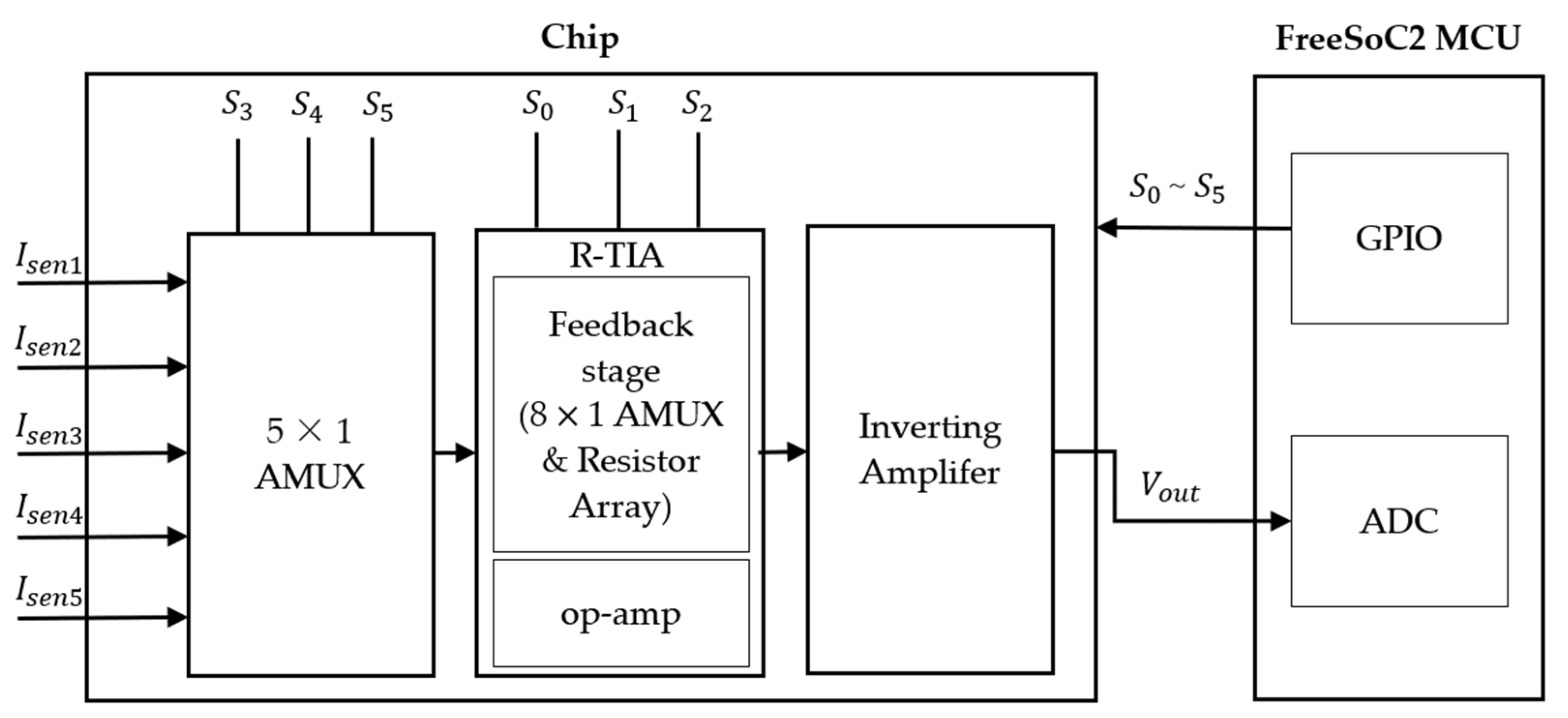
A block diagram of the proposed readout circuit is shown in Figure 2, where the I s e n indicates each sensor’s current output. The circuit consists of an analog multiplexer (AMUX), digitally adjustable TIA, and inverting amplifier. At the input of the circuit, a 5 × 1 AMUX is implemented to interface with five sensors in a single chip. The heart of the proposed readout circuit is a digitally adjustable R-TIA, which is embarked for accurate and wide-ranged I–V conversion. It is comprised of an op–amp and a digitally controlled feedback stage for varying the R f to cover a wide sensor current range. The feedback stage includes an 8 × 1 AMUX and a resistor array containing eight different resistors. Since the R-TIA output is inverted, an additional inverting amplifier is embedded at the last stage to obtain the positive V o u t . An external MCU, “FreeSoC2 development board” (Cypress Semiconductors, San Jose, CA, USA) is utilized to control the selection bits ( S 0 ~ S 5 ) of the AMUXs by general purpose input/output (GPIO) pins. The V o u t is converted to digital form using an internal 16-bit sigma-delta ADC integrated into the MCU.

2.1.1. OP–AMP Design

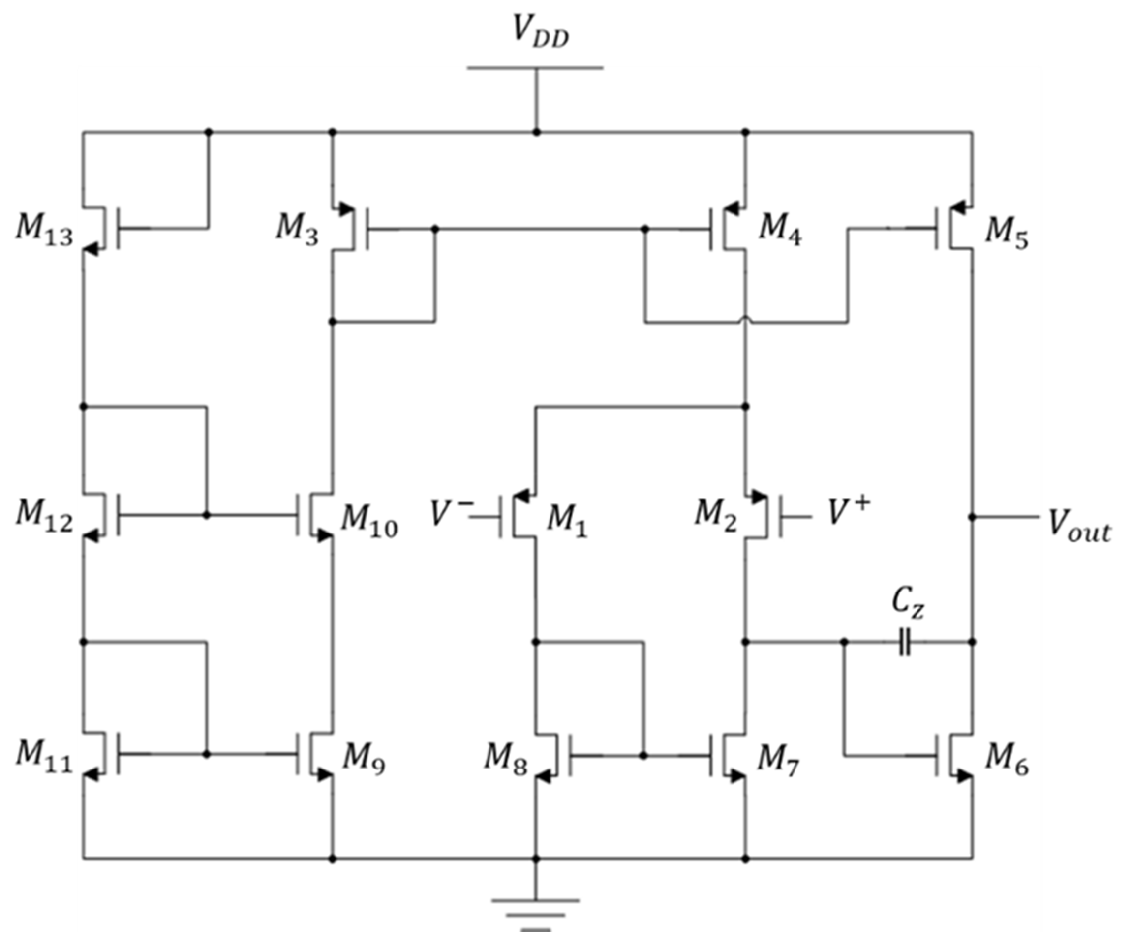
A two-stage op–amp comprising of a bias stage, differential amplifier stage, and common source amplifier stage is designed, as shown in Figure 3. The two-stage op–amp topology usually has the advantage of high gain, high linearity, high output swing, low noise, and good bandwidth. The differential gain stage is introduced, where M 1 forms differential pair with M 2 and a current mirror ( M 7 , M 8 ), as the first stage of the op–amp. The minimum transistor length used in the design is 1 μ m and the differential transistor pair ( M 1 , M 2 ) width is chosen as 32 μ m . A differential input signal applied across the two input terminals ( V , V + ) will be amplified according to the gain of the differential stage. By utilizing current mirror active load transistors ( M 7 , M 8 ), it can have a very large output impedance. The second stage is consisted of M 5 and M 6 transistors with size of 220 μ m and 120 μ m , respectively, which is a common source amplifier for high output swing as the final stage amplifier [42,46]. The transistor pair ( M 3 , M 4 ) is designed as 42 μ m and all the remaining transistor widths are selected as 15 μ m . The cascode current source technique has been implemented to reduce the voltage variations across current source transistors, thus, it can provide accurate current [47]. The first stage gain of the designed op–amp can be represented using Equation (2).
A 1 = g m 1   ( r 02 | | r 07 )
The second stage gain can be expressed as per Equation (3).
A 2 = g m 6   ( r 06 | | r 05 )
By combining Equations (2) and (3), the total gain of the designed op–amp can be described as
A t o t a l = A 1 ×   A 2 =   g m 1   g m 6 ( r 02 | | r 07 ) ( r 06 | | r 05 )
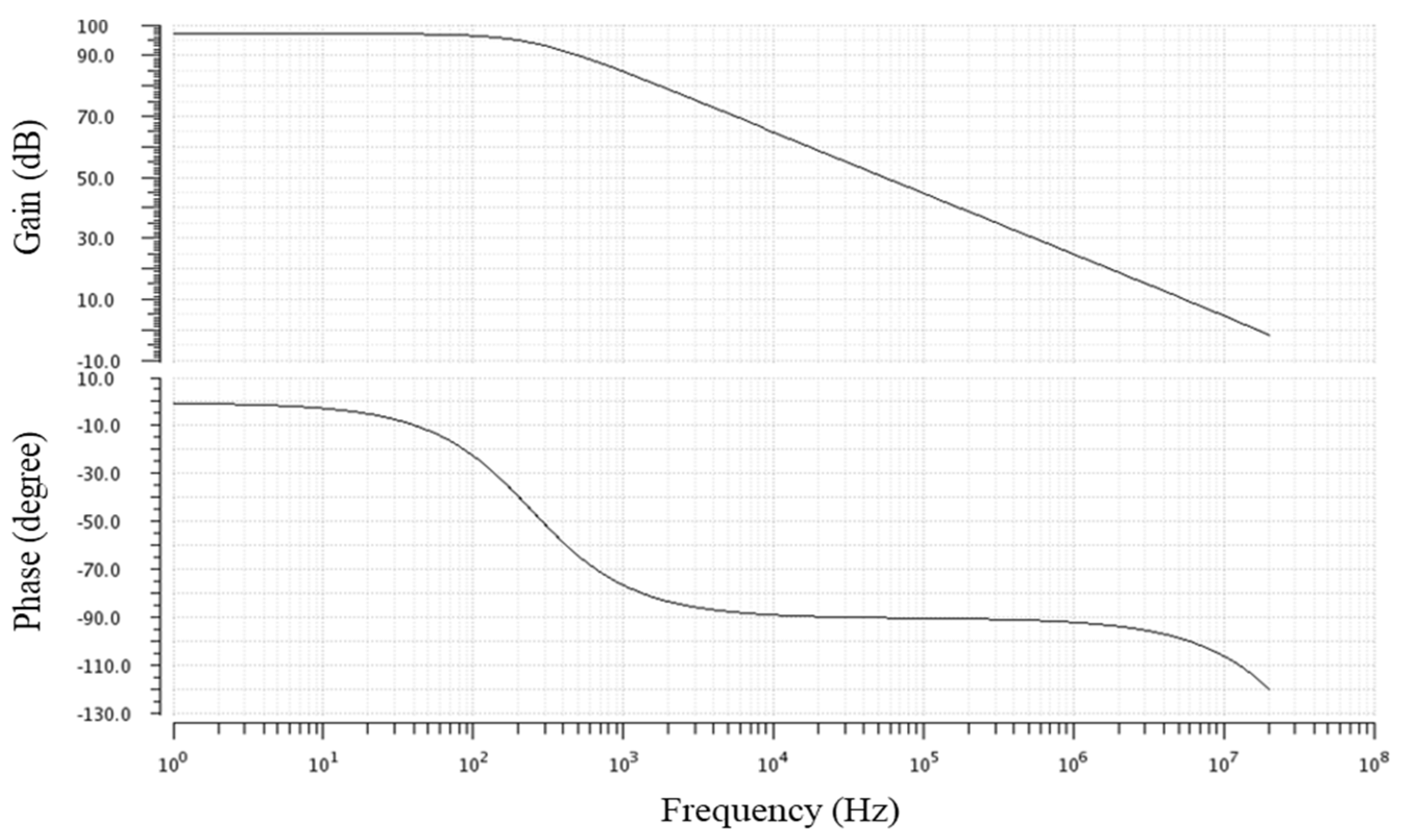
Figure 4 shows the op–amp gain and phase plot during the simulation. For biasing the op–amp, V r e f of 1.65 V is given to M 2 . The op–amp achieves a 97.5 dB gain and 64.05 degrees phase margin as depicted in Figure 4.

2.1.2. Feedback Stage Design

The feedback stage is made up of an 8 × 1 AMUX and resistor array, which includes 10 KΩ, 50 KΩ, 100 KΩ, 200 KΩ, 400 KΩ, 600 KΩ, 800 KΩ, and 1 MΩ resistors. The AMUX is connected in a series with the resistor array to vary the R f by controlling the selection bits of the AMUX, as shown in Figure 5. Each of the I i n in Figure 5 indicates the sensor output current ( I s e n ) that passed through the R f in the resistor array. Depending on the current range of the sensor, the R f value will be altered to avoid the op–amp output swing limitation or accuracy issue due to the ADC resolution. Table 1 shows the sensor current range and the matched value of R f , as per the AMUX selection bits ( S 2 , S 1 , S 0 ).
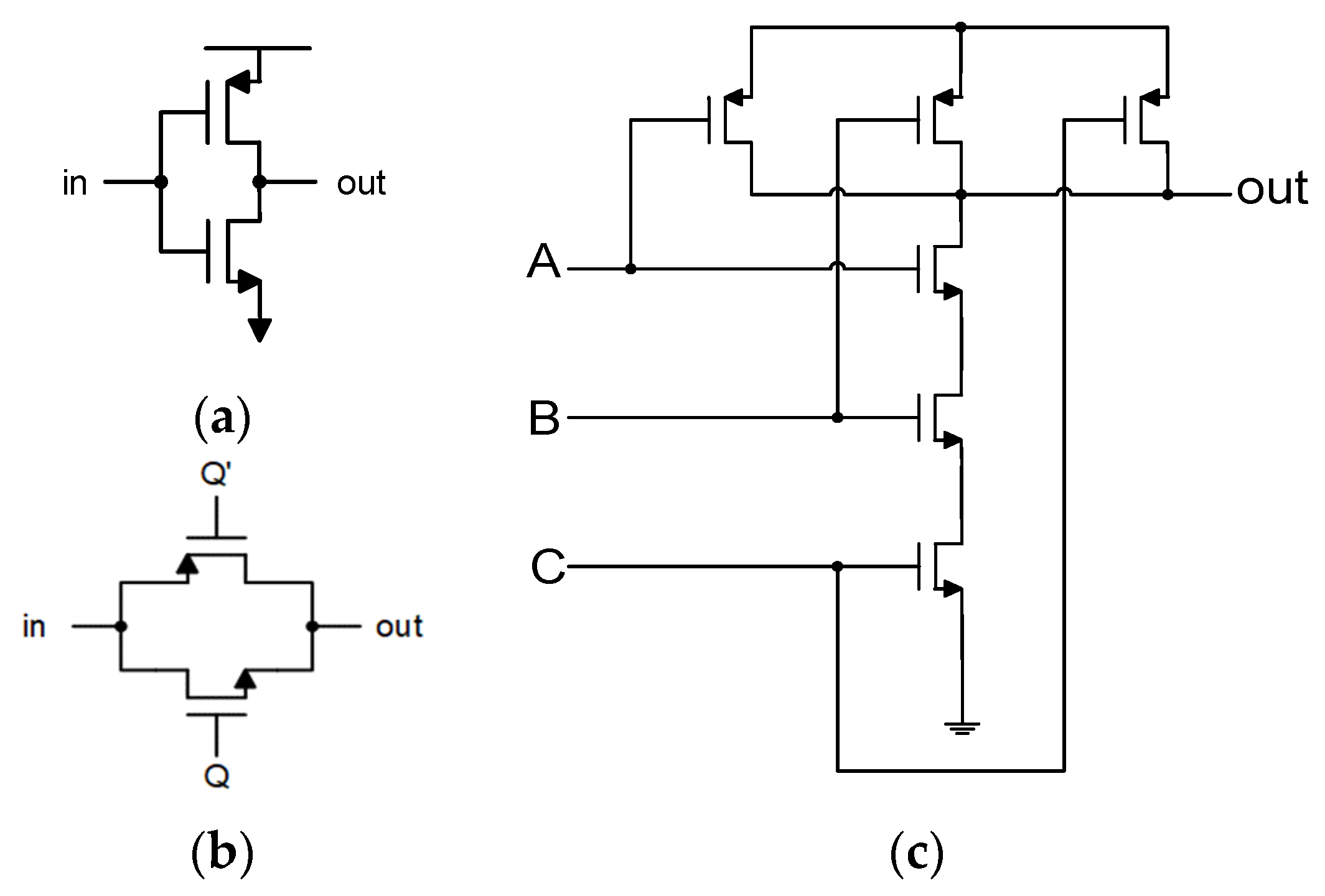
The AMUX is a combinational logic circuit designed to switch one of the several analog input lines through to a single common output line and is controlled by the selection bits. The designed AMUX is composed of: (a) Combinational logic acting as a decoder for the selection bits; and (b) Transmission Gates (TG) for transferring signal from input to output. The combinational logic for decoder is realized with NOT gates and three input NAND gates. The TG, also called as analog switch, can selectively block or pass a signal from its input to output. The TG is comprised of a p-channel metal-oxide semiconductor (PMOS) transistor and a n-channel metal-oxide semiconductor (NMOS) transistor pair. The utilized gates’ schematics are illustrated in Figure 6. The control gate of TG is biased by the control signal in a complementary manner, so both transistors are either on or off. The decoder output ( d o ~ d 7 ) is connected to the control signal of the NMOS transistor, and the inverted decoder output ( d 0 ¯ ~ d 7 ¯ ) is connected to the control signal of the PMOS transistor. An output expression (Out) of the AMUX is represented in Equation (5) and the full schematic of the AMUX is presented in Figure 7.
Out = I i n 0 ( s 2 ¯   s 1 ¯   s 0 ¯ ) + I i n 1 ( s 2   s 1 ¯   s 02 ¯ ) + I i n 2 ( s 2 ¯   s 1   s 0 ¯ ) + I i n 3 ( s 2   s 1   s 0 ¯ ) + I i n 4 ( s 2 ¯   s 1 ¯   s 0 ) + I i n 5 ( s 2   s 1 ¯   s 0 ) + I i n 6 ( s 2 ¯   s 1   s 0 ) + I i n 7 ( s 2   s 1   s 0 )

3. Results and Discussion

3.1. Simulation Results

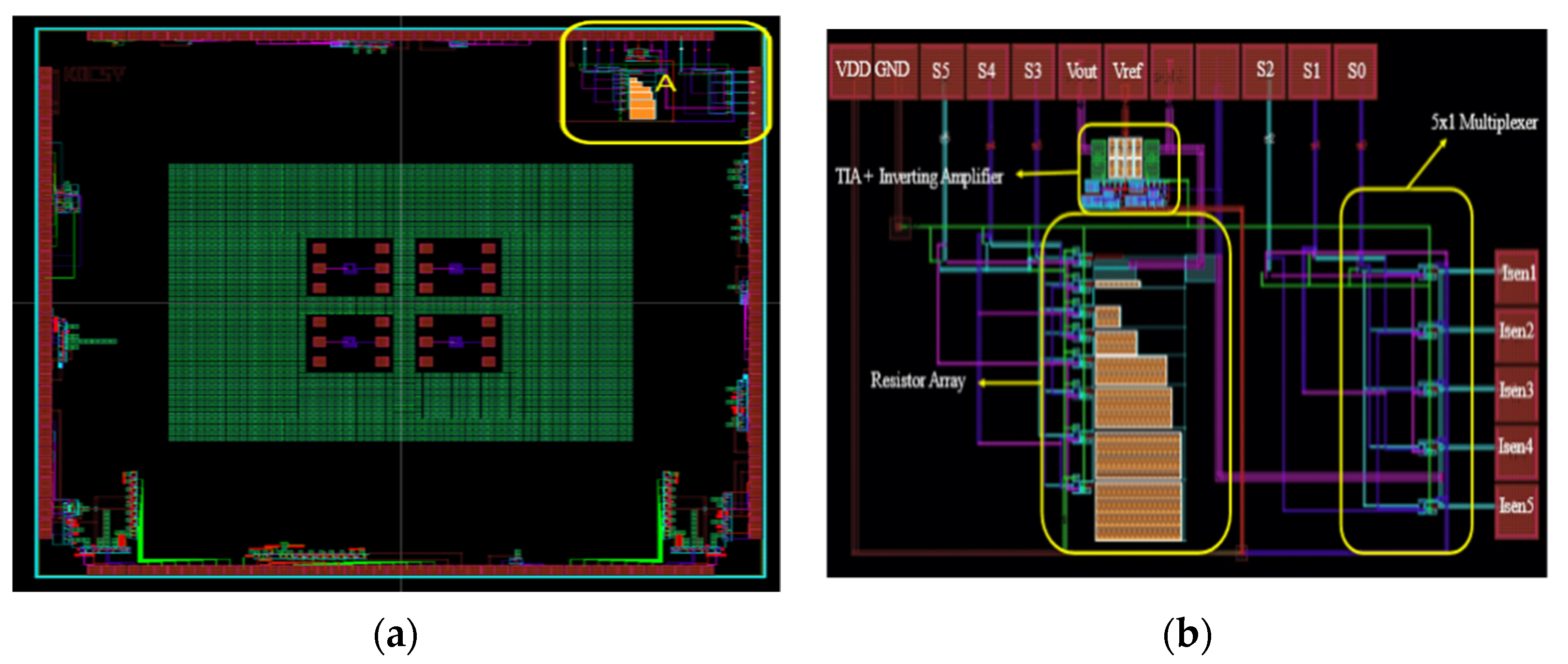
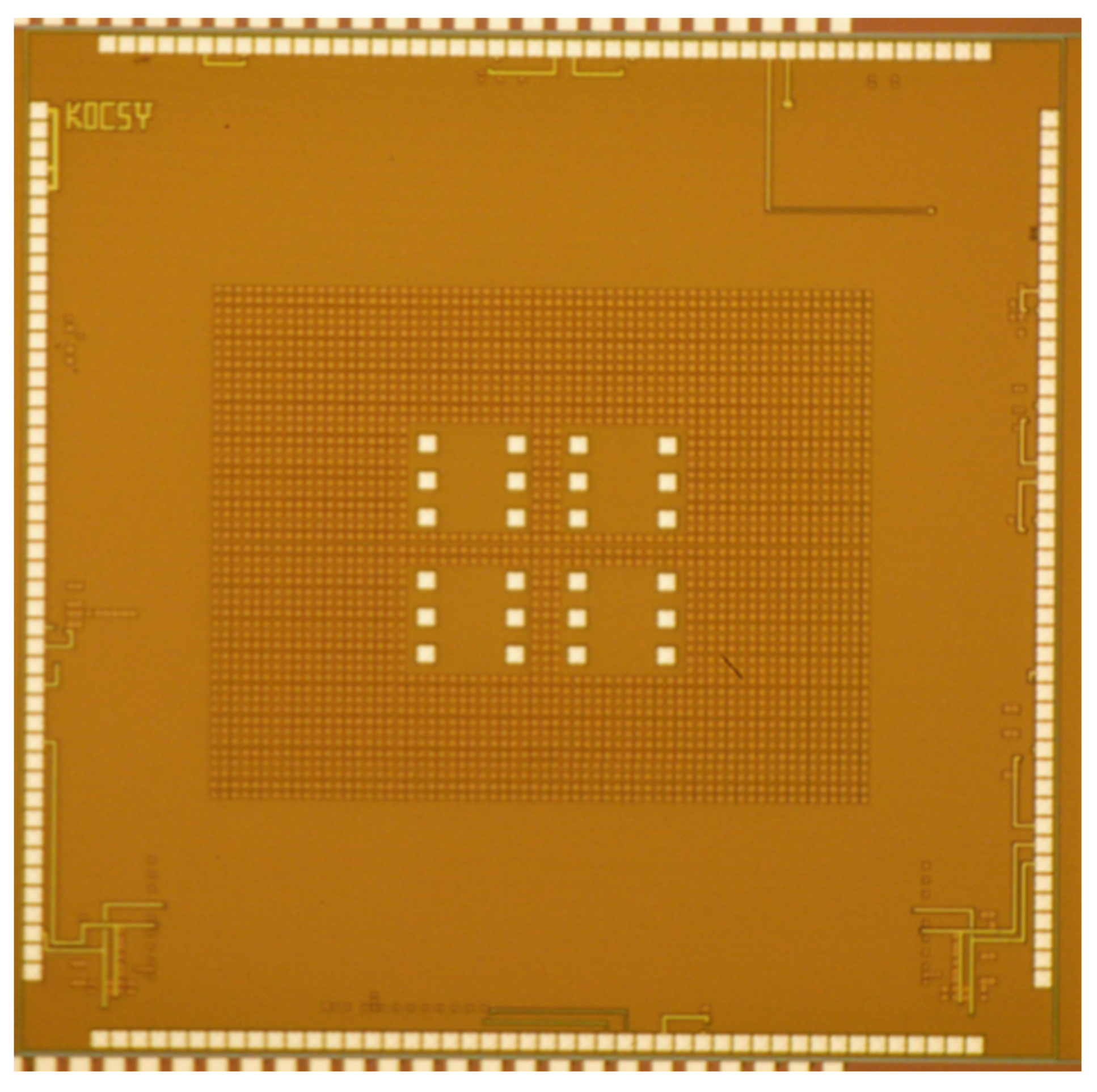
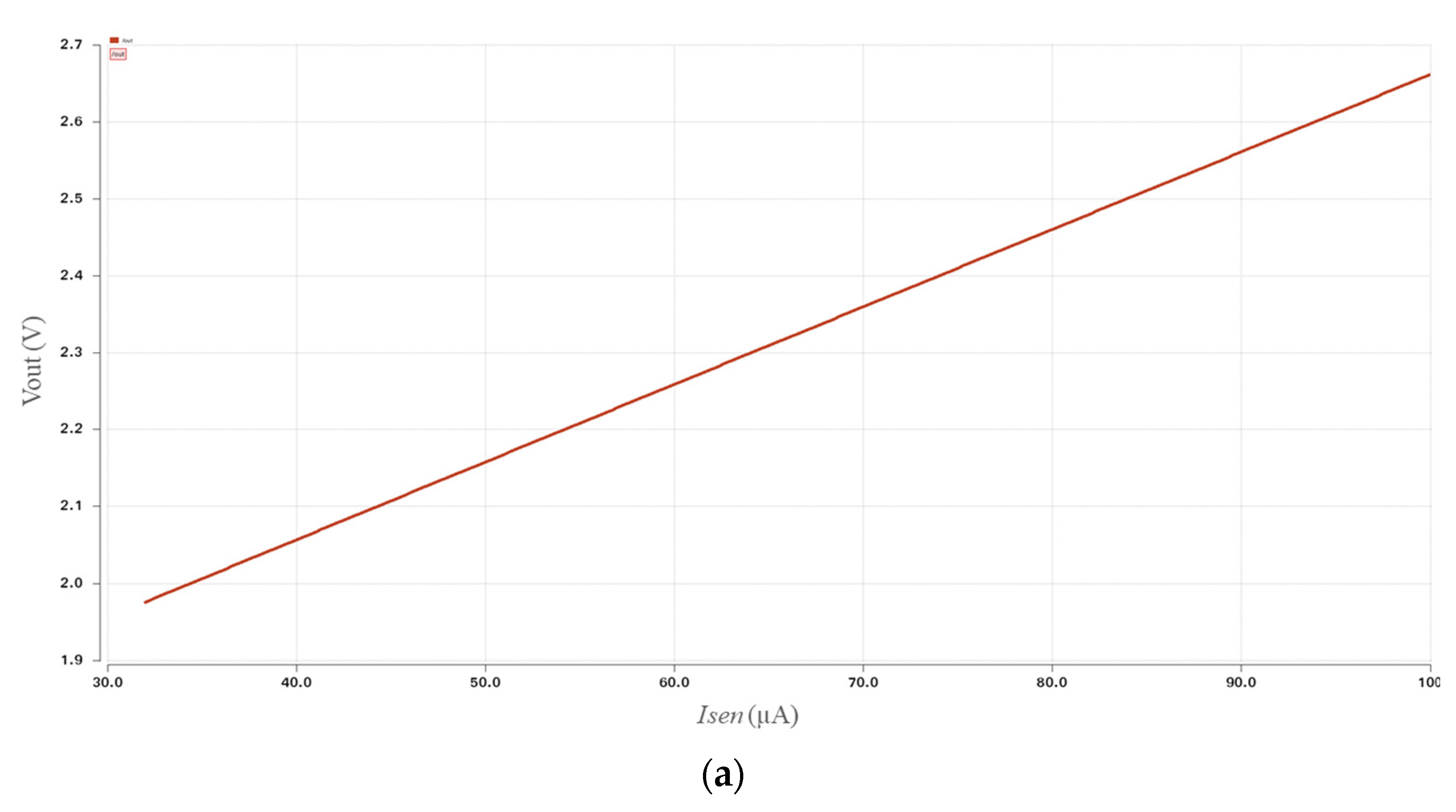
The proposed readout circuit shown in Figure 2 is designed in CMOS 0.18 µm technology utilizing the “Cadence” tool (Cadence Design Systems, San Jose, CA, USA). Figure 8a shows the layout of the complete chip, and Figure 8b illustrates the layout of the proposed architecture, which is the circuit marked as ‘A’ in Figure 8a. The designed circuit occupies an area of 1030 × 620 µm2, including the pads and 580 × 487 µm2, excluding the pads. Figure 9 shows the photo of the fabricated chip. In order to verify the proposed circuit, post simulation of the R-TIA has been conducted. As an example, the simulations were plotted in Figure 10 where R f is 10 KΩ, 100 KΩ, and 1 MΩ, respectively, which cover the minimum and the maximum target range. The Y-axis of the graph in Figure 10 indicates V o u t in unit of volts, while the X-axis represents I s e n in units of µA. The I s e n ranges used for simulations are selected based on Table 1, which are from 32 µA to 100 µA; 8 µA to 12 µA; and 0.1 µA to 1.5 µA when R f values are 10 KΩ, 100 KΩ, and 1 MΩ. The results are well matched with the expected results, which are calculated by Equation (1) and show a linear response throughout the dynamic range. The result demonstrated that the proposed circuit could read signals accurately from electrochemical or biosensor where its current output is within the range 0.1 µA to 100 µA. With the variable R f , the TIA achieved a variable 3 dB bandwidth in the range 3.235 KHz to 225 KHz. Moreover, the TIA exhibits a phase margin of 134.9 ° , 134.8 ° , and 126 ° , when R f is 1 MΩ, 100 KΩ, and 10 KΩ, respectively. Thus, the designed TIA shows a phase margin higher than 45 °   with all R f values in Table 1 indicating the stability of the TIA.

3.2. IC Test Results

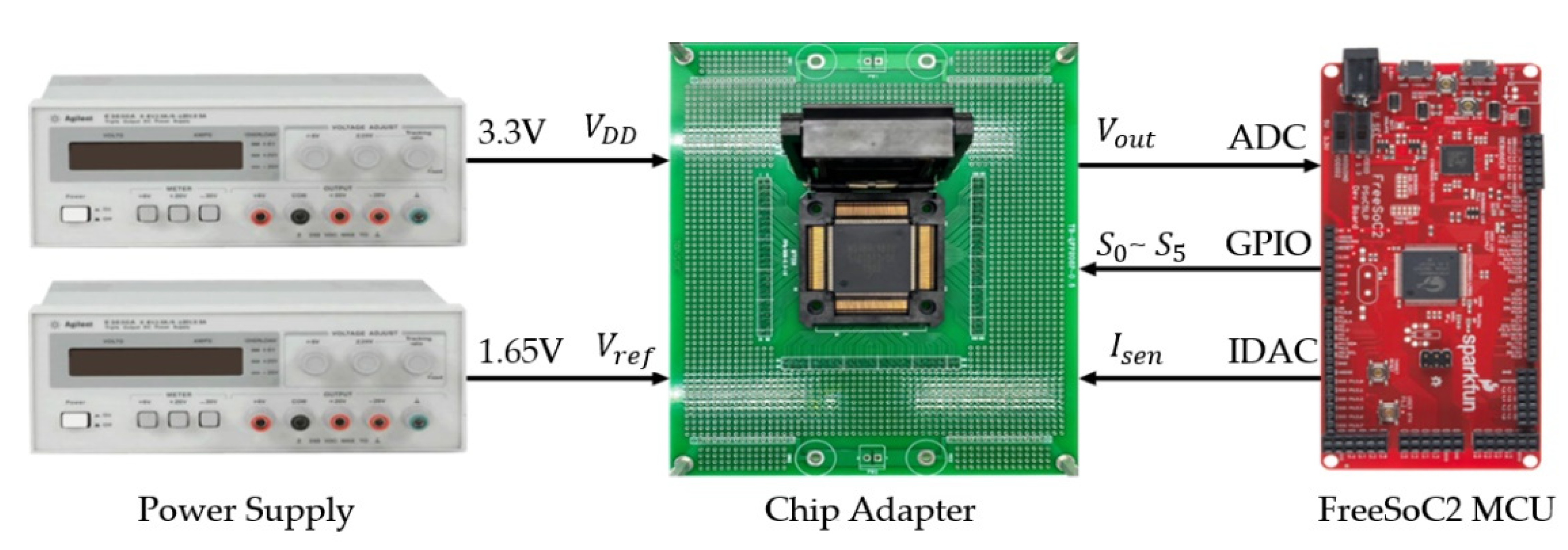
The fabricated chip is packaged with a quad flock package in order to test the chip, and the chip socket is soldered onto an adapter board. The chip is then inserted inside the socket and tested. Figure 11 illustrates the block diagram of the experimental test setup. An “Agilent power supply” (Keysight Technologies, Santa Rosa, CA, USA) is connected to the V D D pin (3.3 V) and the V r e f pin (1.65 V) to power the circuit. To measure the V o u t , a 16-bit sigma-delta ADC embedded in the “FreeSoC2 development board” is utilized. A 16-bit ADC should be able to differentiate 50 µV difference when V D D is 3.3 V. However, the last two or three bits are generally not trustable due to the error from non-ideal characteristics of the ADC, environmental condition, and offset voltage [48]. Thus, a 16-bit ADC can differentiate 400 µV difference in general. An 8-bit Current Digital to Analog Converter (IDAC) implemented in the MCU is connected to the input of the chip to generate and sweep the I s e n for testing the chip. The range of the IDAC in the “FreeSoC2 development board” can be chosen between 2040 µA with an 8 µA resolution and 255 µA with a 1 µA resolution or 31.873 µA with a 0.125 µA resolution. The target current range of this work is from 0.1 µA to 100 µA. Thus, IDAC current ranges of 255 µA with a 1 µA resolution and 31.873 µA with a 0.125 µA resolution were selected as I s e n for testing purpose.
In this work, an algorithm has been developed in the MCU firmware, which can alter the R f automatically, depending on the I s e n range. Figure 12 explains the firmware flowchart of the algorithm. Initially, the R f values are stored in the MCU memory. Once the MCU is on, it selects the AMUX selection bits ( S 2 , S 1 , S 0 ) as (1, 1, 1), which indicates that R f is 1 MΩ and starts to read the ADC voltage. To avoid the clipping issue due to the op–amp output swing limitations, if the ADC value is larger than 3.2 V, it alters the R f with a smaller value until the R f reaches 10 KΩ. If not, the MCU calculates the I s e n value using Equation (1). With this developed firmware, the R f of the R-TIA can be changed automatically depending on the I s e n range, so that the proposed circuit can cover a wide current range of the sensor.
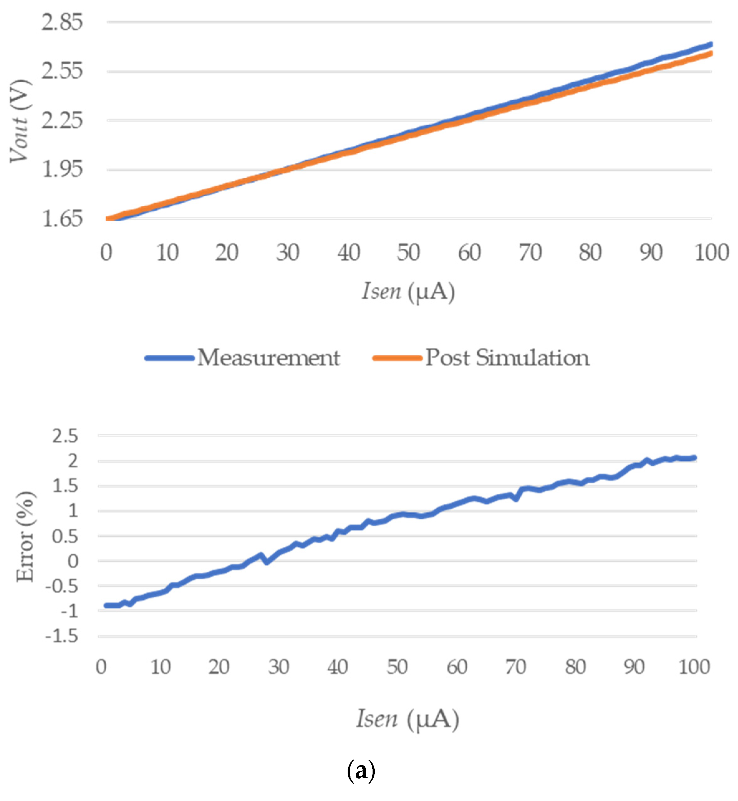
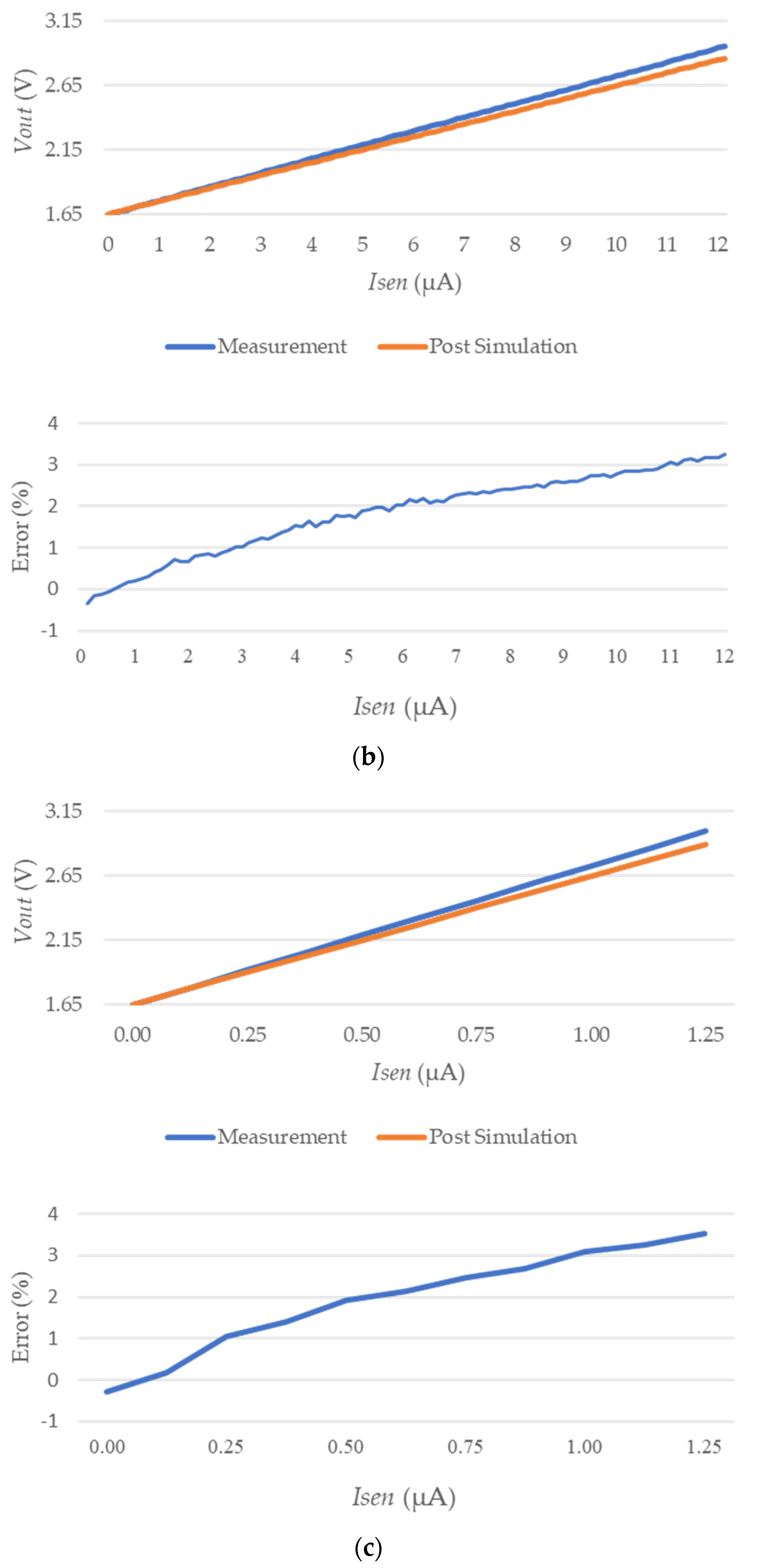
The comparison of the post simulation results and the measurement results during the IC test experiment are recorded in Figure 13, which shows a linear V o u t versus I s e n from 0.1 µA to 100 µA for different values of R f . The error in Figure 13 was calculated by below Equation (6)
E r r o r   ( % ) = V m e a s u r e d V p o s t   s i m u l a t i o n V p o s t   s i m u l a t i o n   × 100
where the V m e a s u r e d is the measured voltage at the ADC and V p o s t   s i m u l a t i o n is the voltage obtained from post simulation. Figure 13 demonstrates an adequately similar output with a slight offset because of the R f error, due to the process resistance tolerance of 2 %, which is fairly linear and can be corrected using the offset correction in the MCU. Thus, the proposed circuit designed in IC is verified that it can cover a wide sensor current range from 0.1 µA to 100 µA. The error rate comparison between the conventional R-TIA with the fixed R f and proposed R-TIA with digitally adjustable R f is conducted and presented in Table 2. For comparison, the R f of the conventional R-TIA is fixed to 10 KΩ, while the R f in the proposed design is altered based on the I s e n range. The measured I s e n in Table 2 are extracted from calculation based on Equation (1). In the case where I s e n is 100 µA, since both methods are using the same R f value, they exhibit a similar error rate. However, when the I s e n is getting smaller, the proposed TIA shows a much better error rate than the conventional R-TIA, as illustrated in the comparison results in Table 2.
A comparison of the proposed readout with existing variable gain TIA architectures is presented in Table 3. Although a wide dynamic range is achieved by the TIA in several architectures, these solutions cannot achieve a linear output across the entire dynamic range. In contrast, the presented TIA showed good linearity throughout the targeted dynamic range, providing a relatively acceptable range. Furthermore, the proposed readout circuit is accomplished by a low power consumption of 0.38 mW and a small area of 0.282 mm 2 , which are important factors for wearable patch type healthcare devices.

4. Conclusions

In this work, the readout circuit consisting of a digitally adjustable R-TIA is designed and fabricated in a 0.18 µm CMOS process for various sensors that have current output. The proposed readout circuit is designed to adopt multiple electrochemical sensors for multifunctional wearable healthcare devices. The auto-adjustable R-TIA is developed to cover a wide range of I s e n by algorithm implemented in the MCU, which is altering the R f value based on the current range. The R-TIA consists of the op–amp and feedback stage. As the R-TIA internal block, the two-stage op–amp is designed that is comprised of a bias stage, differential amplifier stage, and common source amplifier stage; it achieved a 97.5 dB gain and 64.05 degrees phase margin. To make the R f adjustable, a resistor array with an 8 × 1 AMUX is embedded in the R-TIA circuit. The total area of the proposed readout circuit is 1030 µm × 620 µm, including the pads, and its power consumption is 0.38 mW with a power supply of 3.3 V. The measurement result shows that the proposed circuit can cover a wide range of sensor current from 0.1 µA to 100 µA and has an error rate less than 1%.

Author Contributions

Conceptualization, H.P. and S.J.; methodology, H.P. and C.P.; software, H.P.; validation, H.P., S.L. and H.-J.C.; formal analysis, all authors; investigation, H.P. and S.L.; resources, S.J., C.P. and H.-J.C.; data curation, H.P. and S.L.; writing—original draft preparation, S.L.; writing—review and editing, H.P., S.L., S.J., C.P. and H.-J.C.; visualization, S.J.; supervision, S.J. and H.-J.C.; project administration, S.J. and H.-J.C.; funding acquisition, H.-J.C. All authors have read and agreed to the published version of the manuscript.

Funding

This research was supported by Kumoh National Institute of Technology (2018104115).

Data Availability Statement

The datasets generated from the current study are available from the corresponding author on reasonable request.

Conflicts of Interest

The authors declare no conflict of interest.

References

  1. Xie, J.; Chen, Q.; Shen, H.; Li, G. Review—Wearable Graphene Devices for Sensing. J. Electrochem. Soc. 2020, 167, 037541. [Google Scholar] [CrossRef]
  2. Sweeney, D.; Quinlan, L.R.; Browne, P.; Richardson, M.; Meskell, P.; ÓLaighin, G. A Technological Review of Wearable Cueing Devices Addressing Freezing of Gait in Parkinson’s Disease. Sensors 2019, 19, 1277. [Google Scholar] [CrossRef] [PubMed] [Green Version]
  3. Sana, F.; Isselbacher, E.M.; Singh, J.P.; Heist, E.K.; Pathik, B.; Armoundas, A.A. Wearable Devices for Ambulatory Cardiac Monitoring: JACC State-of-the-Art Review. J. Am. Coll. Cardiol. 2020, 75, 1582–1592. [Google Scholar] [CrossRef] [PubMed]
  4. Lutz, W.; Sanderson, W.; Scherbov, S. The coming acceleration of global population ageing. Nature 2008, 451, 716–719. [Google Scholar] [CrossRef]
  5. Dall, T.M.; Gallo, P.D.; Chakrabarti, R.; West, T.; Semilla, A.P.; Storm, M.V. An Aging Population And Growing Disease Burden Will Require ALarge And Specialized Health Care Workforce By 2025. Health Aff. 2013, 32, 2013–2020. [Google Scholar] [CrossRef] [Green Version]
  6. Awais, M.; Palmerini, L.; Bourke, A.K.; Ihlen, E.A.F.; Helbostad, J.L.; Chiari, L. Performance Evaluation of State of the Art Systems for Physical Activity Classification of Older Subjects Using Inertial Sensors in a Real Life Scenario: A Benchmark Study. Sensors 2016, 16, 2105. [Google Scholar] [CrossRef] [Green Version]
  7. Vijayalakshmi, K.; Uma, S.; Bhuvanya, R.; Suresh, A. A demand for wearable devices in health care. Int. J. Eng. Technol. 2018, 7, 1. [Google Scholar] [CrossRef] [Green Version]
  8. Engel, J.M.; Mehta, V.; Fogoros, R.; Chavan, A. Study of Arrhythmia Prevalence in NUVANT Mobile Cardiac Telemetry System Patients. In Proceedings of the 2012 Annual International Conference of the IEEE Engineering in Medicine and Biology Society, San Diego, CA, USA, 28 August–1 September 2012; pp. 2440–2443. [Google Scholar]
  9. Barrett, P.M.; Komatireddy, R.; Haaser, S.; Topol, S.; Sheard, J.; Encinas, J.; Fought, A.J.; Topol, E.J. Comparison of 24-h Holter Monitoring with 14-day Novel Adhesive Patch Electrocardiographic Monitoring. Am. J. Med. 2014, 127, 95.e11–95.e17. [Google Scholar] [CrossRef] [Green Version]
  10. Altini, M.; Casale, P.; Penders, J.; ten Velde, G.; Plasqui, G.; Amft, O. Cardiorespiratory fitness estimation using wearable sensors: Laboratory and free-living analysis of context-specific submaximal heart rates. J. Appl. Physiol. 2016, 120, 1082–1096. [Google Scholar] [CrossRef]
  11. Digiglio, P.; Li, R.; Wang, W.; Pan, T. Microflotronic Arterial Tonometry for Continuous Wearable Non-Invasive Hemodynamic Monitoring. Ann. Biomed. Eng. 2014, 42, 2278–2288. [Google Scholar] [CrossRef]
  12. Etemadi, M.; Inan, O.T. Wearable ballistocardiogram and seismocardiogram systems for health and performance. J. Appl. Physiol. 2017, 124, 452–461. [Google Scholar] [CrossRef] [PubMed]
  13. Lau, J.K.; Lowres, N.; Neubeck, L.; Brieger, D.B.; Sy, R.W.; Galloway, C.D.; Albert, D.E.; Freedman, S.B. iPhone ECG application for community screening to detect silent atrial fibrillation: A novel technology to prevent stroke. Int. J. Cardiol. 2013, 165, 193–194. [Google Scholar] [CrossRef] [PubMed]
  14. Sohn, K.; Merchant, F.M.; Abohashem, S.; Kulkarni, K.; Singh, J.P.; Heist, E.K.; Owen, C.; Roberts, J.D., Jr.; Isselbacher, E.M.; Sana, F.; et al. Utility of a smartphone based system (cvrphone) to accurately determine apneic events from electrocardiographic signals. PLoS ONE 2019, 14, e0217217. [Google Scholar] [CrossRef] [PubMed]
  15. Yoon, S.; Sim, J.K.; Cho, Y.H. A Flexible and Wearable Human Stress Monitoring Patch. Sci. Rep. 2016, 6, 23468. [Google Scholar] [CrossRef] [Green Version]
  16. Lakshminarayana, S.; Park, Y.; Park, H.; Jung, S. High Density Resistive Array Readout System for Wearable Electronics. Sensors 2022, 22, 1878. [Google Scholar] [CrossRef]
  17. Sempionatto, J.R.; Lin, M.; Yin, L.; De la Paz, E.; Pei, K.; Sonsa-Ard, T.; de Loyola Silva, A.N.; Khorshed, A.A.; Zhang, F.; Tostado, N.; et al. An epidermal patch for the simultaneous monitoring of haemodynamic and metabolic biomarkers. Nat. Biomed. Eng. 2021, 5, 737–748. [Google Scholar] [CrossRef]
  18. Li, X.; He, L.; Li, Y.; Chao, M.; Li, M.; Wan, P.; Zhang, L. Correction to “Healable, Degradable and Conductive MXene Nanocomposite Hydrogel for Multifunctional Epidermal Sensor”. ACS Nano 2021, 15, 12453. [Google Scholar] [CrossRef]
  19. Xi, W.; Yeo, J.C.; Yu, L.; Zhang, S.; Lim, C.T. Ultrathin and Wearable Microtubular Epidermal Sensor for Real-Time Physiological Pulse Monitoring. Adv. Mater. Technol. 2017, 2, 1700016. [Google Scholar] [CrossRef]
  20. Yoon, S.; Yoon, H.; Zahed, M.A.; Park, C.; Kim, D.; Park, J.Y. Multifunctional hybrid skin patch for wearable smart healthcare applications. Biosens. Bioelectron. 2022, 196, 113685. [Google Scholar] [CrossRef]
  21. Imani, S.; Bandodkar, A.J.; Mohan, A.M.V.; Kumar, R.; Yu, S.; Wang, J.; Mercier, P.P. A wearable chemical–electrophysiological hybrid biosensing system for real-time health and fitness monitoring. Nat. Commun. 2016, 7, 11650. [Google Scholar] [CrossRef]
  22. Mariam El, G.; Fernández-García, R.; Ahyoud, S.; Gil, I. A Review of Flexible Wearable Antenna Sensors: Design, Fabrication Methods, and Applications. Materials 2020, 13, 3781. [Google Scholar]
  23. Li, R.; Qi, H.; Ma, Y.; Deng, Y.; Liu, S.; Jie, Y.; Jing, J.; He, J.; Zhang, X.; Wheatley, L.; et al. A flexible and physically transient electrochemical sensor for real-time wireless nitric oxide monitoring. Nat. Commun. 2020, 11, 3207. [Google Scholar] [CrossRef] [PubMed]
  24. Liu, J.; Lu, W.; Zhang, L.; Yang, J.; Yao, Z.-P.; He, Y.; Li, Y. Integrated hand-held electrochemical sensor for multicomponent detection in urine. Biosens. Bioelectron. 2021, 193, 113534. [Google Scholar] [CrossRef] [PubMed]
  25. Pan, Y.; Zuo, J.; Hou, Z.; Huang, Y.; Huang, C. Preparation of Electrochemical Sensor Based on Zinc Oxide Nanoparticles for Simultaneous Determination of AA, DA, and UA. Front. Chem. 2020, 8, 2538. [Google Scholar] [CrossRef]
  26. Ma, R.; Liu, M.; Zheng, H.; Zhu, Z. A 66-dB Linear Dynamic Range, 100-dB·Ω Transimpedance Gain TIA With High-Speed PDSH for LiDAR. IEEE Trans. Instrum. Meas. 2020, 69, 1020–1028. [Google Scholar] [CrossRef]
  27. Micusik, D.; Zimmermann, H. 130dB-DR Transimpedance Amplifier with Monotonic Logarithmic Compression and High-Current Monitor. In Proceedings of the 2008 IEEE International Solid-State Circuits Conference—Digest of Technical Papers, San Francisco, CA, USA, 3–7 February 2008; pp. 78–597. [Google Scholar]
  28. Mičušík, D.; Zimmermann, H. Transimpedance amplifier with 120 dB dynamic range. Electron. Lett. 2007, 43, 159–160. [Google Scholar] [CrossRef]
  29. Aznar, F.; Gaberl, W.; Zimmermann, H. A highly sensitive 2.5 Gb/s transimpedance amplifier in CMOS technology. In Proceedings of the 2009 IEEE International Symposium on Circuits and Systems, Taipei, Taiwan, 24–27 May 2009; pp. 189–192. [Google Scholar]
  30. Atef, M.; Hassan, O.; Awwad, F.; Khan, M.A.B. High Dynamic Range Photocurrent Sensory Circuit with a Multi-Transistor Background Light Cancellation Loop for Photoplethysmography Sensing. Electronics 2021, 10, 2769. [Google Scholar] [CrossRef]
  31. Wang, W.; Sonkusale, S. An Approach for a Wide Dynamic Range Low-Noise Current Readout Circuit. J. Low Power Electron. Appl. 2020, 10, 23. [Google Scholar] [CrossRef]
  32. Rad, R.E.; Hejazi, A.; Asl, S.-A.H.; Shehzad, K.; Verma, D.; Kim, S.; Rikan, B.S.; Pu, Y.; Kim, J.T.; Hwang, K.C.; et al. A 77-dB Dynamic-Range Analog Front-End for Fine-Dust Detection Systems with Dual-Mode Ultra-Low Noise TIA. Sensors 2021, 21, 6360. [Google Scholar] [CrossRef]
  33. Hsu, C.; Hall, D.A. A current-measurement front-end with 160dB dynamic range and 7ppm INL. In Proceedings of the 2018 IEEE International Solid—State Circuits Conference—(ISSCC), San Francisco, CA, USA, 11–15 February 2018; pp. 326–328. [Google Scholar]
  34. Dai, S.; Perera, R.T.; Yang, Z.; Rosenstein, J.K. A 155-dB Dynamic Range Current Measurement Front End for Electrochemical Biosensing. IEEE Trans. Biomed. Circuits Syst. 2016, 10, 935–944. [Google Scholar] [CrossRef]
  35. Ferrari, G.; Gozzini, F.; Molari, A.; Sampietro, M. Transimpedance Amplifier for High Sensitivity Current Measurements on Nanodevices. IEEE J. Solid-State Circuits 2009, 44, 1609–1616. [Google Scholar] [CrossRef]
  36. Hsu, C.L.; Jiang, H.; Venkatesh, A.G.; Hall, D.A. A Hybrid Semi-Digital Transimpedance Amplifier with Noise Cancellation Technique for Nanopore-Based DNA Sequencing. IEEE Trans. Biomed. Circuits Syst. 2015, 9, 652–661. [Google Scholar] [CrossRef] [PubMed]
  37. Goldstein, B.; Kim, D.; Rottigni, A.; Xu, J.; Vanderlick, T.K.; Culurciello, E. CMOS low current measurement system for biomedical applications. IEEE Trans. Biomed. Circuits Syst. 2012, 6, 1017–1020. [Google Scholar] [CrossRef] [PubMed]
  38. Kim, J.; Maitra, R.; Pedrotti, K.D.; Dunbar, W.B. A Patch-Clamp ASIC for Nanopore-Based DNA Analysis. IEEE Trans. Biomed. Circuits Syst. 2013, 7, 285–295. [Google Scholar] [CrossRef]
  39. Lu, J.; Holleman, J. A Wideband Ultra-Low-Current On-Chip Ammeter. In Proceedings of the IEEE 2012 Custom Integrated Circuits Conference, San Jose, CA, USA, 9–12 September 2012; pp. 1–4. [Google Scholar]
  40. Bennati, M.; Thei, F.; Rossi, M.; Crescentini, M.; Avino, G.D.; Baschirotto, A.; Tartagni, M. 20.5 A Sub-pA ΔΣ Current Amplifier for Single-Molecule Nanosensors. In Proceedings of the 2009 IEEE International Solid-State Circuits Conference—Digest of Technical Papers, San Francisco, CA, USA, 8–12 February 2009; pp. 348–349, 349a. [Google Scholar]
  41. Crescentini, M.; Thei, F.; Bennati, M.; Saha, S.; de Planque, M.R.; Morgan, H.; Tartagni, M. A Distributed Amplifier System for Bilayer Lipid Membrane (BLM) Arrays With Noise and Individual Offset Cancellation. IEEE Trans Biomed. Circuits Syst. 2015, 9, 334–344. [Google Scholar] [CrossRef] [Green Version]
  42. Qiao, H. Design of a CMOS Two-stage Fully Differential Operation Amplifier. J. Phys. Conf. Ser. 2020, 1449, 012084. [Google Scholar] [CrossRef]
  43. Ciofi, C.; Crupi, F.; Pace, C.; Scandurra, G.; Patane, M. A New Circuit Topology for the Realization of Very Low-Noise Wide-Bandwidth Transimpedance Amplifier. IEEE Trans. Instrum. Meas. 2007, 56, 1626–1631. [Google Scholar] [CrossRef]
  44. Chuah, J.H.; Holburn, D. Design of Low-Noise High-Gain CMOS Transimpedance Amplifier for Intelligent Sensing of Secondary Electrons. IEEE Sens. J. 2015, 15, 5997–6004. [Google Scholar] [CrossRef]
  45. Säckinger, E. Analysis and Design of Transimpedance Amplifiers for Optical Receivers; John Wiley & Sons: Hoboken, NJ, USA, 2017; pp. 207–278. [Google Scholar] [CrossRef]
  46. Zihong, L.; Chao, B.; Zhihua, W.; Chun, Z. Full Custom Design of a Two-Stage Fully Differential CMOS Amplifier with High Unity-Gain Bandwidth and Large Dynamic Range at Output. In Proceedings of the 48th Midwest Symposium on Circuits and Systems, Covington, KY, USA, 7–10 August 2005; Volume 982, pp. 984–987. [Google Scholar]
  47. Ramirez-Angulo, J.; Sawant, M.S.; López-Martín, A.; Carvajal, R.G. Compact implementation of high-performance CMOS current mirror. Electron. Lett. 2005, 41, 570. [Google Scholar] [CrossRef]
  48. Balestrieri, E.; Daponte, P.; Rapuano, S. A state of the art on ADC error compensation methods. IEEE Trans. Instrum. Meas. 2005, 54, 1388–1394. [Google Scholar] [CrossRef]
Figure 1. Circuit of conventional resistive Transimpedance Amplifier (R-TIA).
Electronics 11 01181 g001
Figure 2. Block diagram of the proposed readout.
Electronics 11 01181 g002
Figure 3. Schematic of the designed operational amplifier (op–amp).
Electronics 11 01181 g003
Figure 4. Op–amp gain and phase plot.
Electronics 11 01181 g004
Figure 5. Block diagram of the feedback stage.
Electronics 11 01181 g005
Figure 6. Schematic of (a) NOT gate; (b) Transmission Gate (TG); (c) NAND gate.
Electronics 11 01181 g006
Figure 7. Schematic of an analog multiplexer (AMUX).
Electronics 11 01181 g007
Figure 8. (a) Layout of the fabricated chip; (b) layout of the proposed readout circuit.
Electronics 11 01181 g008
Figure 9. Photo of the fabricated chip.
Electronics 11 01181 g009
Figure 10. Simulation results illustrating the voltage output ( V o u t ) versus sensor curent ( I s e n ) with different feedback resistors ( R f ) (a) R f = 10 KΩ; (b) R f = 100 KΩ; (c) R f   = 1 MΩ.
Electronics 11 01181 g010aElectronics 11 01181 g010b
Figure 11. Block diagram of the experimental test setup.
Electronics 11 01181 g011
Figure 12. Firmware flowchart embedded in the Microcontroller Unit (MCU).
Electronics 11 01181 g012
Figure 13. Comparison graphs of V o u t versus I s e n and error between the measurement result and post simulation result when (a) R f = 10 KΩ; (b) R f = 100 KΩ; and (c) R f = 1 MΩ.
Electronics 11 01181 g013aElectronics 11 01181 g013b
Table 1. Feedback resistor selection with sensor current range.
S 2 S 1 S 0 Feedback Resistor
R f (KΩ)
Sensor Current
Range I s e n (µA)
0001032~100
0015012~32
0101008~12
0112004~8
1004002.5~4
1016002~2.5
1108001.5~2
11110000.1~1.5
Table 2. Extracted I s e n   and error rates with the conventional TIA and proposed TIA.
Expected I s e n
(A)
Measured I s e n with Conventional TIA (A)Measured I s e n with Proposed TIA (A)Error Rate of Conventional TIA (%)Error Rate of Proposed TIA (%)
100 µ100.48 µ100.48 µ0.480.48
10 µ13.32 µ10.069 µ33.2780.698
1 µ2.253 µ1.005 µ125.30.5
Table 3. Comparison of the proposed readout with existing architectures.
Ref.Input Current Range
(A)
Input
Dynamic Range
(dB)
Power Consumption (mW)Transimpedance Gain Range
(dBΩ)
Supply Voltage
(V)
TechnologyArea mm2Error Rate
(%)
Our work0.1 µ–100 µ600.3860–1203.30.18 µm CMOS0.2821
[26]1 µ–2 m662154–1003.30.18 µm CMOS0.3560.40
[31]100 f–1 μ14010.3N/A1.80.18 µm CMOS1.015N/A
[32]N/A772.71N/A3.30.18 µm CMOS1.21N/A
[38]4.21 p–369 n98.90.5138–1681.50.35 µm CMOS0.3N/A
Publisher’s Note: MDPI stays neutral with regard to jurisdictional claims in published maps and institutional affiliations.