Article

Fault Tolerance Analysis of Five-Level Neutral-Point-Clamped Inverters under Clamping Diode Open-Circuit Failure

1
GREEN, Université de Lorraine, F-54500 Nancy, France
2
CNRS, IJL, Université de Lorraine, F-54500 Nancy, France
3
The Center of Excellence for Power Systems Automation and Operation, Department of Electrical Engineering, Iran University of Science and Technology, Tehran 1311416846, Iran
*
Author to whom correspondence should be addressed.
Electronics 2022, 11(9), 1461; https://doi.org/10.3390/electronics11091461
Submission received: 30 March 2022 / Revised: 25 April 2022 / Accepted: 28 April 2022 / Published: 3 May 2022
(This article belongs to the Special Issue Advances in Fault Detection/Diagnosis of Electrical Power Devices)

Abstract

:
Multilevel inverters are increasingly used in industrial applications in which service continuity is crucial. This paper presents an original approach to ensure the fault-tolerant operation of neutral-point-clamped (NPC) inverters in the case of an open-circuit fault event in a clamping diode, which is rarely investigated in the conducted research work. The proposed fault-tolerant strategy meets the following criteria: restoring rated output voltage and current during post-fault operation, realizing fault-tolerant operation without additional components, maintaining rated total harmonic distortion (THD) during fault-tolerant operation, and fast transition between faulty operation and remedial operation. In the proposed approach, prior to applying the appropriate remedial action, identification of the defective clamping diode is required. In this respect, a very fast and simple logic-based fault diagnosis is presented whose implementation does not need any additional components and external circuit. Moreover, it does not require any component modeling and complicated calculations. The proposed strategy is validated by simulation and experimentation.

1. Introduction

Multilevel inverters have been attracting wide attention in industry for some decades. These inverters have the following advantages: reduced total harmonic distortion, limited losses, reduced voltage transient, and smaller size of filter components. Thus, they provide major advantages, compared with two-level topologies [1,2]. Any transformers or flying capacitors are not used in neutral-point-clamped (NPC) topologies; thus, these circuits are increasingly used in industry. Nevertheless, in high-voltage applications, unequal voltage sharing increases [3]. To cope with this problem, NPC/H-bridge topology is preferred to classical NPC circuits. In order to constitute an NPC/H-bridge inverter from the topology of a three-phase three-level NPC inverter, each phase or leg of the classical NPC circuit is substituted by a single-phase five-level NPC module (see Figure 1a). Thus, as depicted in Figure 1a, each phase has its own DC link capacitors. Providing the independent DC voltage sources necessitates employing a transformer with a rectifier for each NPC module of the three-phase circuit, which complicates the structure of this type of inverter compared with the classical NPC inverter. This can be considered as a small disadvantage for this NPC/H-bridge inverter structure.
In NPC topology, clamping diodes have a key role to generate output voltage levels. In this circuit, solely the clamping diodes connect the inverter leg to the neutral point, whereas in the other topologies such as T-type or active-NPC (ANPC), this connection is carried out by power switches. In addition, the clamping diodes are not immune to failure. When an open-circuit fault occurs in a clamping diode, the output current and voltage distortion increase. In addition, the DC link capacitor voltages would differ significantly from the nominal value, which leads the capacitors to breakdown. Hence, identifying the defective clamping diode and subsequently applying an appropriate fault-tolerant strategy is mandatory to suppress the previously mentioned consequences and ensure service continuity in the nominal mode. However, in most of the research studies, identifying a faulty clamping diode and ensuring the service continuity in case of breakdown are overlooked. In the majority of the research efforts dealing with fault diagnosis and fault-tolerant operation in NPC inverters, the identification approaches mainly concern the power switches, and they are based on the hypothesis that clamping diodes never break down. Thus, when an open-circuit fault appears in a clamping diode, erroneous fault detection and subsequently erroneous remedial actions are applied, according to the published open-circuit switch fault diagnosis algorithms, or the fault detection cannot be carried out. Consequently, the system operates under fault condition without remedial operation. Furthermore, these proposed diagnosis methods cannot be developed and generalized to provide fault diagnosis and appropriate service continuity when a clamping diode breaks down. In this regard, ensuring the fault-tolerant operation in the case of open-circuit failure in a clamping diode is rarely investigated, but it is of considerable importance. Previous research work is mainly classified into two categories. The work in the first category solely proposes the remedial operation subsequent to the fault diagnosis.
The studies included in the second category only propose the fault diagnosis method and do not deal with fault-tolerant operation. It should be noted that there are a few of papers that treat fault diagnosis and fault-tolerant operation together.
Regarding the first category, the research work presented in [4,5,6,7] proposes a switch fault-tolerant approach for three-level NPC converters, but these strategies are not able to guarantee continuity of service when a clamping diode is faulty. More particularly, in the research work presented in [1,8], the authors investigated the continuity of service of an NPC inverter. However, the proposed approach to ensure the continuity of service when a clamping diode breaks down was not studied. In [9], an open-circuit fault-tolerant approach for an NPC inverter is also examined. The strategy ensures the service continuity of the inverter when a clamping diode is faulty (open circuit). In this paper, in order to generate the desired voltage level at the terminal of the inverter, the infeasible switching states are replaced by the possible ones, and the dwell time of the switching states is changed. Nevertheless, service continuity is performed in degraded mode, by applying two-level switching instead of three-level switching. Consequently, the total harmonic distortion of the output current is increased, compared with those in healthy operation. In [10], under clamping diode failure, the service continuity of an NPC inverter is accomplished without redundant components. In the case of fault occurrence, by utilizing the inherent characteristics of the three-level NPC inverter, the impossible control orders are replaced with the available ones. After remedial actions, the inverter is not able to deliver the rated power because the desired voltage amplitude cannot be generated at the terminal. In [11], authors studied remedial actions when a clamping diode is faulty (open circuit). Without employing any redundant leg, the rated terminal voltage is generated using inherent redundancy of the inverter, but the total harmonic distortion of the output voltage and output current is increased.
Concerning the second category, the research work presented in [12,13,14,15,16,17,18] deals with switch fault diagnosis in NPC inverters but cannot locate an open-circuit fault in a clamping diode. In [12], according to the Average Current Park’s Vector, the faulty phase can be identified. However, the faulty switch and the defective clamping diode cannot be identified by this approach. By employing average Current Park’s Vector strategy in [13], the faulty switch is pinpointed in a three-phase NPC circuit, but this presented approach cannot locate a defective clamping diode. In [14], in accordance with the current patterns resulting from an open-switch fault event in a three-phase NPC inverter and the duration of zero current, a faulty switch can be located. The defective clamping diode cannot be identified. The approach presented in [15] is only able to identify the defective phase in a three-phase NPC inverter. In addition, pole voltage measurement is carried out using additional sensors and circuits. The approach proposed in [16] can identify a defective switch by comparing the measured pole voltage and estimated pole voltage for a three-phase NPC rectifier. Moreover, this method cannot identify the defective clamping diode.
The authors of [19] present a fault diagnosis strategy that necessitates employing three extra sensors to measure the pole voltages to pinpoint a defective clamping diode in an NPC inverter. In [9], based on the analysis carried out on the distorted current resulting from a faulty clamping diode (open circuit) in NPC converters, the defective phase is determined. Then, by injecting the under-excited current, the faulty diode is pinpointed. In the particular case of a single-phase NPC/H-bridge converter [20], the authors proposed an approach based on the estimation of the grid current. Then, in all possible cases for open-circuit failures in clamping diodes, the fault diagnosis is accomplished by analyzing the generated residual value. Here, the grid parameters such as the transformer inductance and resistance are required. In [21], a clamping diode fault diagnosis is carried out by analyzing the electromagnetic emissions. This method requires external antennas and filters.
This paper comprises two major parts concerning a single-phase five-level NPC inverter. The first one deals with the fault diagnosis to finally perform fault-tolerant operation. The second part presents the remedial actions. The proposed diagnosis approach encompasses several superiorities compared to the research studies mentioned in the literature. For fault diagnosis, employing extra sensors and hardware and complicated calculations and modeling is avoided. Moreover, the proposed diagnosis method does not rely on the load or grid parameters. Moreover, it can be implemented on field-programmable gate array (FPGA), and high time performances can be obtained. Furthermore, the proposed fault detection method is not affected by system imperfections and measurement errors. Above all, the faulty clamping diode can be identified fast and efficiently, which is seldom seen in past research work. The second section concentrates on the fault-tolerant operation when an open-circuit fault occurs in a clamping diode. The presented approach offers several paramount advantages. To realize the remedial operation, no additional components or bidirectional switches are utilized. Moreover, the nominal power can be delivered during the fault-tolerant operation, and the output current and output voltage are not changed or deteriorated in terms of distortion after remedial actions.
In Section 2, we introduce the fault diagnosis approach we propose. In the third section, the continuity of service is detailed. In Section 4, we present and discuss the simulation results. Selected experimental results are provided and discussed in Section 5. Finally, in the last section, we conclude this paper.

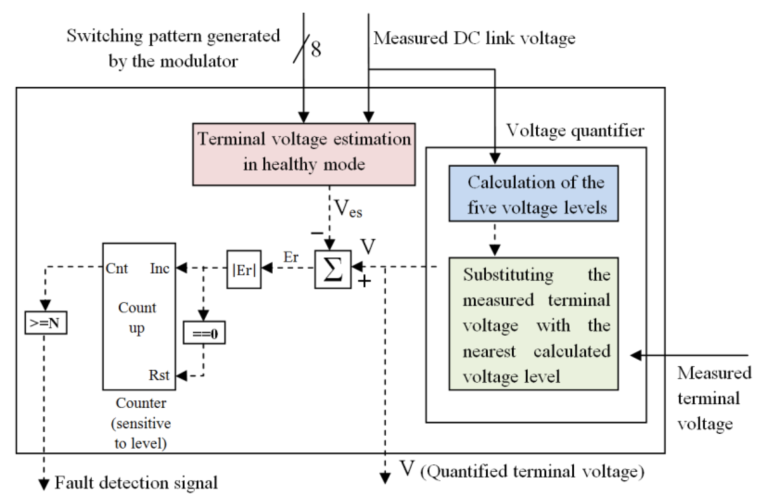
2. Principle of the Clamping Diode Fault Diagnosis Approach

Prior to remedial actions, the faulty component has to be identified. The fault diagnosis approach is constituted of two stages. In stage one, the fault occurrence is detected. In the second stage, called fault localization, following fault detection, the defective component is pinpointed. The scheme of the studied NPC circuit is depicted in Figure 1b. The conducting components during each switching state and the corresponding control orders are tabulated in Table 1 and Table 2, respectively.

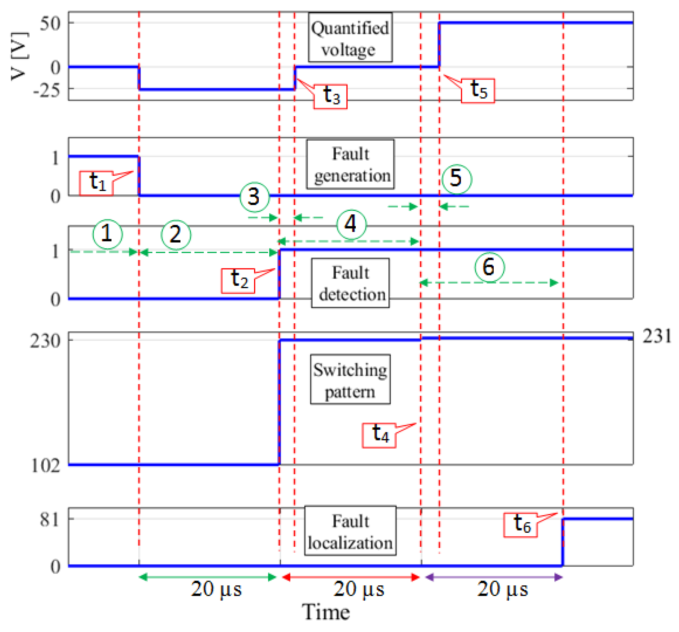
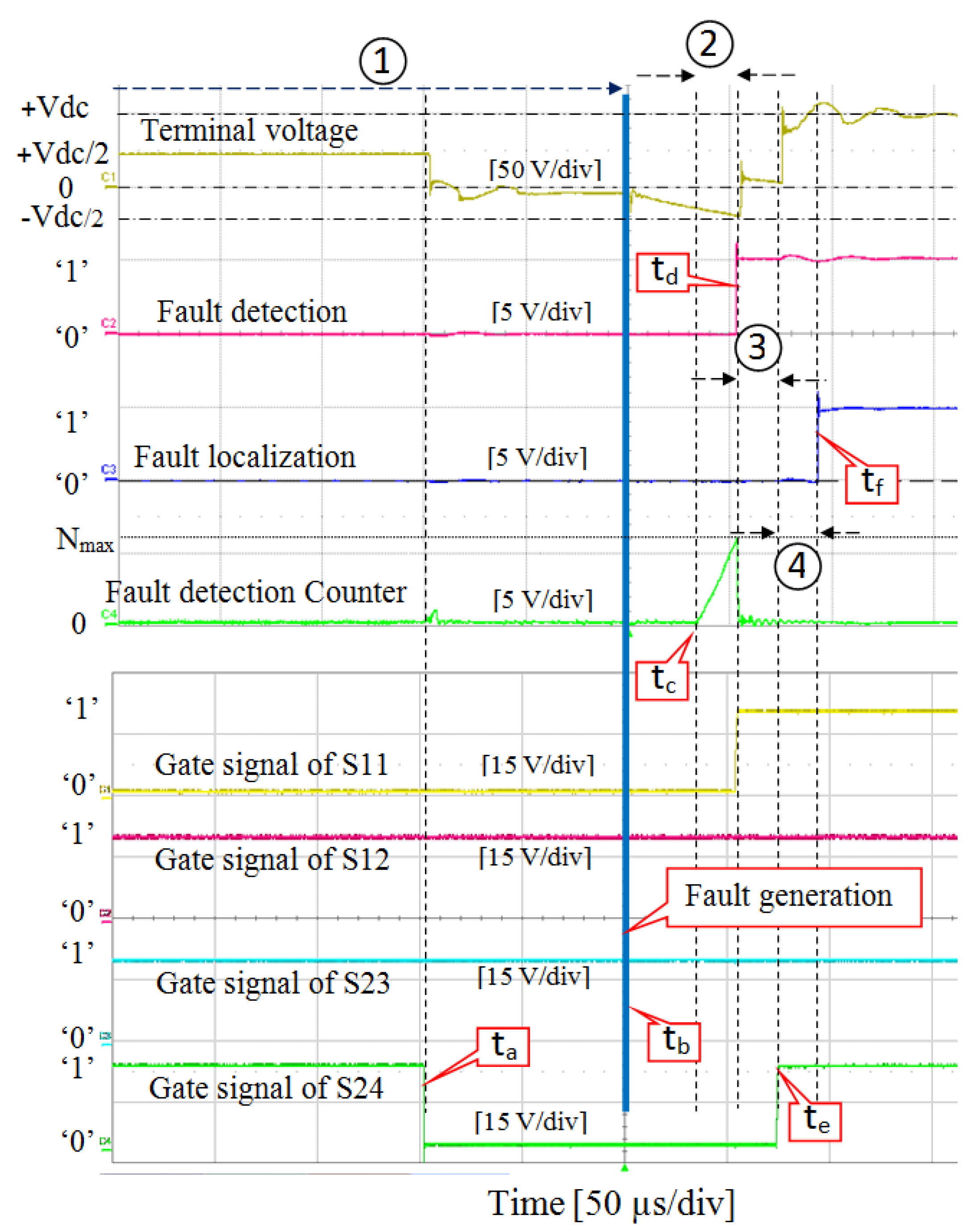
2.1. Fault Detection Strategy

The fault detection approach relies on the measured and estimated output voltage. Based on the value of the DC link voltage and the applied control orders, the output voltage value is estimated. In more detail, as illustrated in Figure 2, the fault detection phase includes two parts. The first part deals with the voltage quantification. Even in healthy operation, the measured and estimated output voltage values are different, due to the measurement errors and voltage drop across the conducting components and the terminal current.
The five possible terminal voltage levels are calculated from the DC link voltage value. Then, the voltage quantifier assigns the nearest calculated voltage level to the measured terminal voltage, whose value is replaced by the quantified voltage, calculated from the same DC link voltage value (see Figure 2) used for output voltage estimation. In this way, false fault detection due to the above-mentioned errors is avoided. By means of the voltage quantifier, in contrast to [22], an accurate estimation of this voltage error is not needed. The second part is the counter. Because of the dead times and delays around the switching instants, the measured and estimated terminal voltage values are different. If this difference subsists beyond a certain time value (upper limit time of the counter called Nmax), it means that this difference arises from a fault event. Otherwise, this difference is caused by the dead times and delays. The upper limit time of the counter (Nmax) is fixed according to the total delay times of the components presented by the manufacturer, which is set at 20 µs in this study.

2.2. Fault Localization Strategy

Following fault detection, the clamping diode fault localization begins. We propose to use a failure mode analysis for the fault localization strategy. Applying this method allows us to locate a defective clamping diode by considering that the fault either occurred in a clamping diode or in a power switch. In this regard, Table 3 and Table 4 gather all the cases of open-circuit faults in all components. Since the studied structure is symmetric, the fault localization is solely explained when the output current is positive.
The failure mode analysis, allowing for the identification of a faulty component, is summarized in Table 3 and Table 4. The third column (from left) in Table 3 is obtained by supposing an open-circuit fault in each component for all the switching states. The presented topology includes four clamping diodes (DC1, DC2, DC3, and DC4), four external switches (S11, S14, S21, and S24), and four internal switches (S12, S13, S22, and S23). If an open-circuit fault event occurs in the external switches, the clamping diode located in the same half-leg forms the current path rather than the defective external switch. If an open-circuit failure occurs in the internal switches or in the clamping diodes, the output current flows through the two antiparallel diodes situated in the opposite half-leg instead of the faulty internal switch or the defective clamping diode. In this way, the third column (from left) is obtained for all switching states and components forming the current path corresponding to each switching state. According to the last applied control orders, the quantified output voltage is compared with the estimated voltages presented in the third column (from left). Thus, the faulty component is identified. If the quantified terminal voltage is equal to more than one estimated voltage, the faulty component is not identified distinctly. Thus, it is mandatory to perform the next step. In the second step, the switching state is modified, and the new components forming the current path accompanying the corresponding terminal voltages are indicated in the fifth column (from left) of Table 3. Once again, the quantified terminal voltage is compared with the estimated voltages. Similar to the previous step, if necessary, the third step should be carried out. The results obtained after performing the third step are provided in Table 4. According to Table 3 and Table 4, in order to identify the defective clamping diode, performing two or three steps is needed. In the simulation section, by giving an example, the applied fault localization strategy is clarified.

3. Principle of the Proposed Fault-Tolerant Strategy

In the following subsections, the modification of the switching states to be performed to realize the continuity of service is explained.

3.1. Open-Circuit Fault in DC1 or DC2

Based on Table 1, in switching states 3, 5, and 7, the output current flows through DC1 (positive current) or DC2 (negative current). Thus, if an open-circuit fault occurs in DC1 or DC2, the expected terminal voltages corresponding to switching states 3, 5, and 7 are not achievable. In this regard, as represented in Table 5, switching state 3 is substituted by switching state 2 to attain the terminal +Vdc/2. As shown in Table 1, in switching state 2 (regardless of the sign of the output current), the output current does not pass through DC1 or DC2. Hence, the terminal voltage can attain +Vdc/2, as desired. Switching state 5 can be substituted by switching state 4 or switching state 6 in which no clamping diode conducts the output current. We mentioned here that switching states 4 and 6 have a similar impact on the voltages of the neutral point and the DC link capacitors because in switching state 4 or switching state 6 (see Table 1) there is no current injected to the neutral point. Therefore, 0 V is made at the terminal either by substituting switching state 4 or switching state 6. In order to obtain an output voltage equal to −Vdc/2, switching state 7 is replaced by switching state 8. As mentioned in Table 5, in switching state 8, the terminal current does not pass through the clamping diodes DC1 or DC2.

3.2. Open-Circuit Fault in DC3 or DC4

As shown in the preceding subsection, Table 5 is established corresponding to the faulty clamping diodes DC3 or DC4. In case of fault occurrence in DC3 or DC4, the switching states 2, 5, and 8 are replaced by the switching states 3, 4 or 6, and 7, respectively. It should be noticed that in case of open-circuit failure in DC3 or DC4, switching state 4 or switching state 6 can be applied interchangeably because no current flows into the neutral point in both cases.

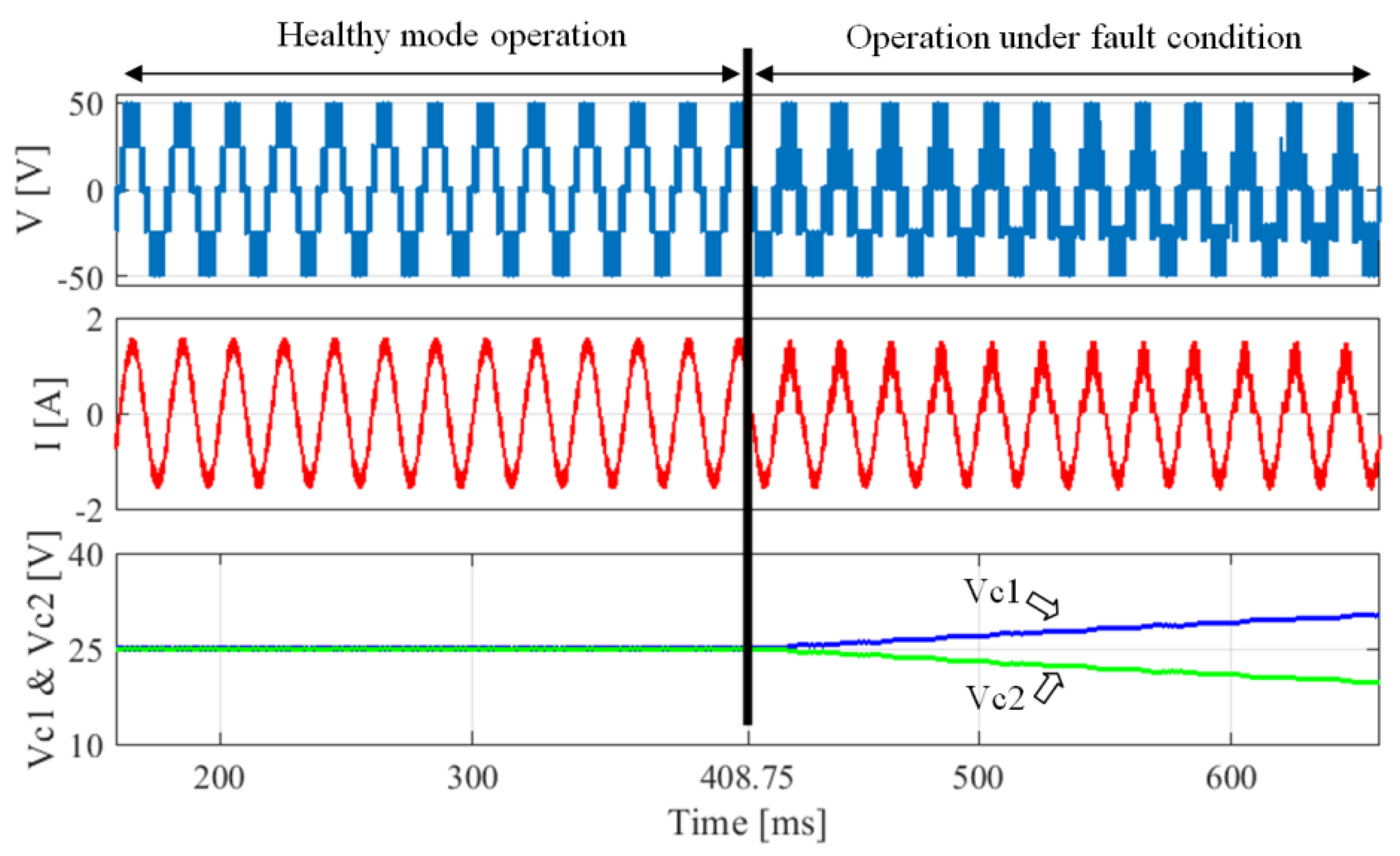
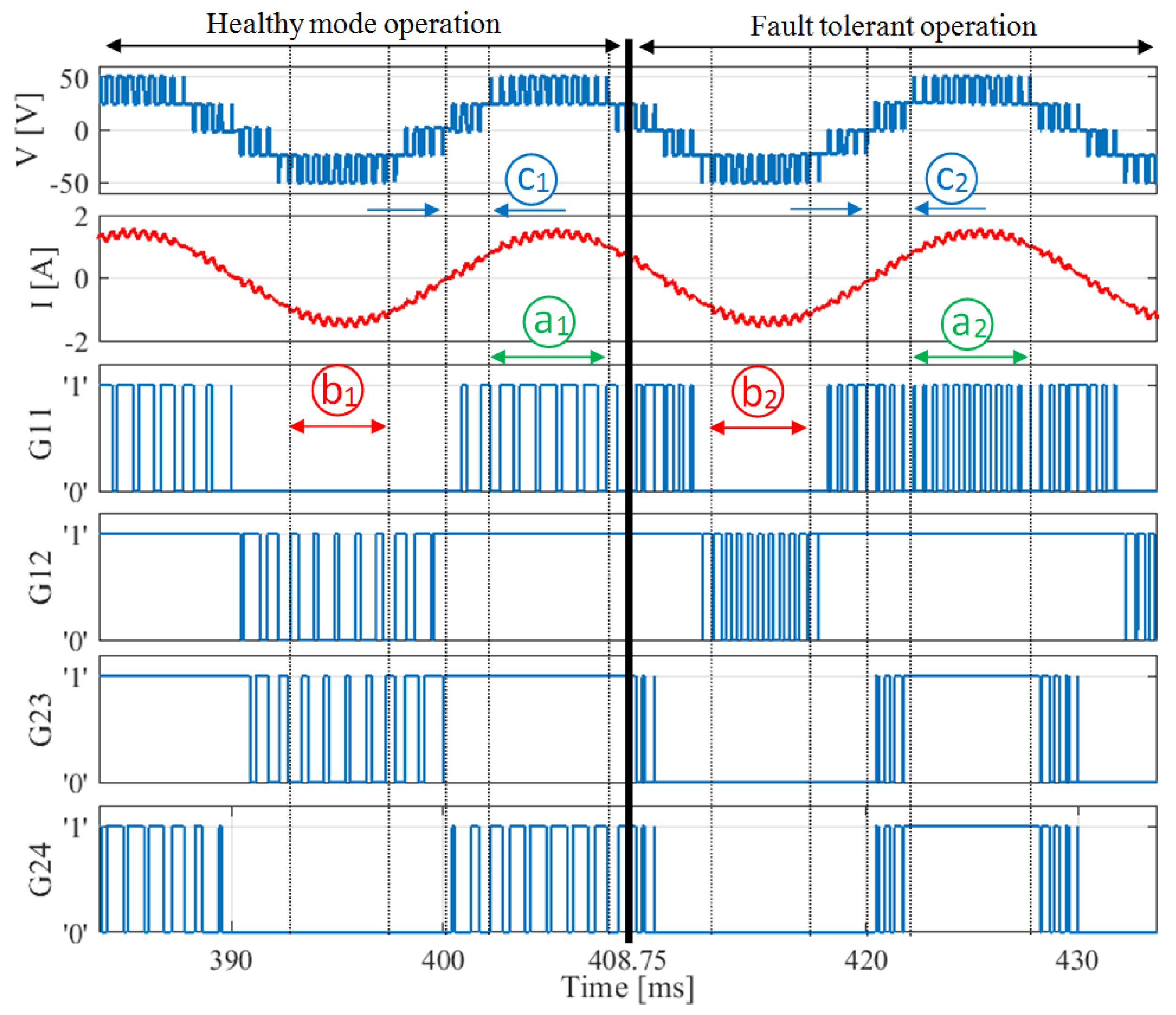
4. Simulation Results

Some selected simulation results are represented in the following. First, fault diagnosis is discussed. In the second subsection, some results about the applied fault-tolerant strategy are elaborated. Since the topology of the converter is symmetric, clamping diode DC4 was chosen as the faulty component. The simulation parameters are summarized in Table 6.

4.1. Fault Diagnosis Strategy

Depending on the last applied switching state in healthy conditions, the faulty component can be identified in the first, second, or third steps (Table 3 and Table 4). In order to avoid presenting similar results, we chose to detail the most complicated case study. In this regard, DC4 was considered as the faulty component. In Figure 3, we present the fault localization procedure for the clamping diode DC4. In order to better represent the defective component in the simulations, we attributed decimal numbers to the power switches and clamping diodes. We attributed to S11, S12, S13, S14, S21, S22, S23, S24, DC1, DC2, DC3, and DC4, the numbers 128, 64, 32, 16, 8, 4, 2, 1, 3, 9, 27, and 81, respectively. As represented in Figure 3, before instant t1 (interval 1), the converter is in normal operation, and the output voltage and switching state attain 0 V and 102 (switching state 5). Hence, right before the failure in DC4 (instant t1), the current chooses DC1, S12, S23, and DC4. As the generated open-circuit fault occurs in DC4 at instant t1, the quantified voltage takes −Vdc/2, in accordance with Table 3. Then, the fault is detected at instant t2. However, the localization of the defective component is still not possible because in accordance with Table 3, in cases where an open-circuit fault occurs in S12, DC1, S23, or DC4, the same quantified voltage −Vdc/2 results at the first step. Therefore, the execution of the second step is required in which the power switch S11 is turned on once the fault detection signal is generated at instant t2 as can be seen in Figure 3. Once S11 conducts, the current path in accordance with Table 3 is constituted by S11, S12, D22, and D11. Hence, the quantified voltage attains 0 at instant t3 because of the dead time of the drivers (interval 3). Based on the corresponding subsection in Table 3, after the first modification of the switching pattern (the second step), the quantified terminal voltages resulted by open-circuit fault occurrence in S23 and DC4 are the same and equal to 0 V.
Thus, it is not possible to determine the defective component (between S23 and DC4) after performing the second step. Thus, performing the third step is indispensable. To this end, according to Figure 3, at instant t4, the third step S24 is switched on. After passing interval 5, the quantified terminal voltage is equal to +Vdc at instant t5. Based on the failure-mode analysis summarized in Table 4, the defective diode DC4 is pinpointed at instant t6.

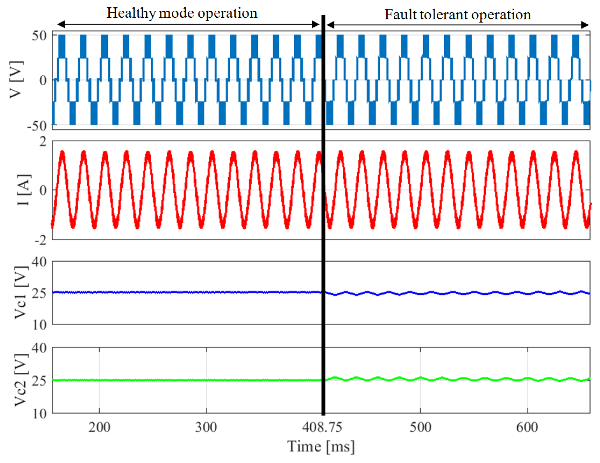
4.2. Fault-Tolerant Strategy

Subsequent to the identification of the defective clamping diode explained in the previous subsection, remedial operation of the inverter begins. To perform continuity of service, we used an approach that does not require any additional or redundant components. Solely by modification of certain switching states (used in healthy conditions—see Table 5), service continuity is ensured. Figure 4 illustrates the case of an open-circuit failure in DC4, without applying a fault-tolerant strategy. One can notice that the two DC link capacitor voltages start to differ from their nominal values, and the output voltage and current are deteriorated in terms of distortion. In the case of the fault event in DC4, the proposed remedial actions are illustrated in Figure 5 and Figure 6. It should be noted that in Figure 5 and Figure 6, the interval between the fault occurrence and the triggering of the fault tolerant operation (faulty component identification) is not visible because according to the results presented in Figure 3, this interval lasts 60 µs, which is not large enough to be seen in Figure 5 and Figure 6. As shown in Figure 5, during post-fault operation, the output voltage and current are the same as those during healthy operation. Moreover, despite low-frequency oscillation with negligible ripple amplitude in the DC link capacitor voltages, the neutral point voltage is stabilized. In Figure 6, the modifications of the switching states are represented.
In this respect, the switching states corresponding to the same output voltage levels during healthy operation and fault-tolerant operation are compared. In Figure 6, the gate signals G11, G12, G23, and G24 represent the applied switching state. The other gate signals are complementary to the selected ones. Hence, according to the aforementioned gate signals, the corresponding switching state can be obtained. During healthy operation (interval a1), the output voltage levels +Vdc and +Vdc/2 are made. By referring to Table 2, switching states 1, 2, and 3 are applied in this interval. During interval a2, the same output voltage levels (+Vdc and +Vdc/2) are obtained compared with interval a1, but the switching state 2 is substituted with switching state 3. Indeed, over the entire interval a2, G12, G23, and G24 are set at ‘1’, and only G11 is toggled between ‘0’ and ‘1’, which complies with Table 5. In accordance with the data summarized in Table 2, switching states 1, 2, and 3 are applied during this interval. In accordance with the output voltage levels acquired during interval b1 (−Vdc and −Vdc/2) and by referring to Table 2, one can deduce that switching states 7, 8, and 9 are applied in this interval. By comparing the gate signals applied in interval b2 (fault-tolerant operation) with those applied in interval b1, it is deduced that state 8 is substituted by state 7 (G11, G23, and G24 are set at ‘0’, and G12 is toggled between ‘0’ and ‘1’). Likewise, one can notice that switching states 2 and 5 are substituted with switching states 3 and 4, respectively.

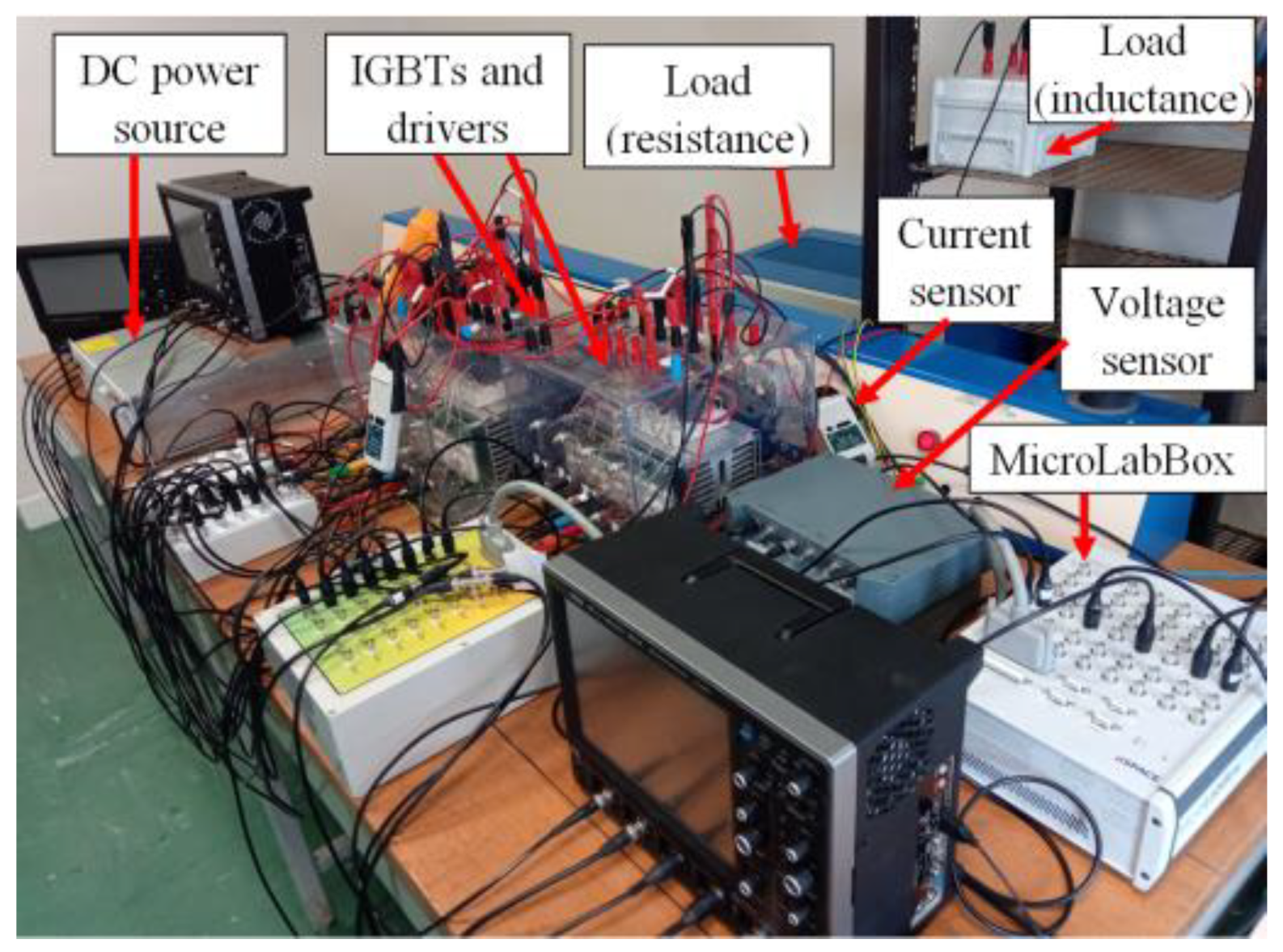
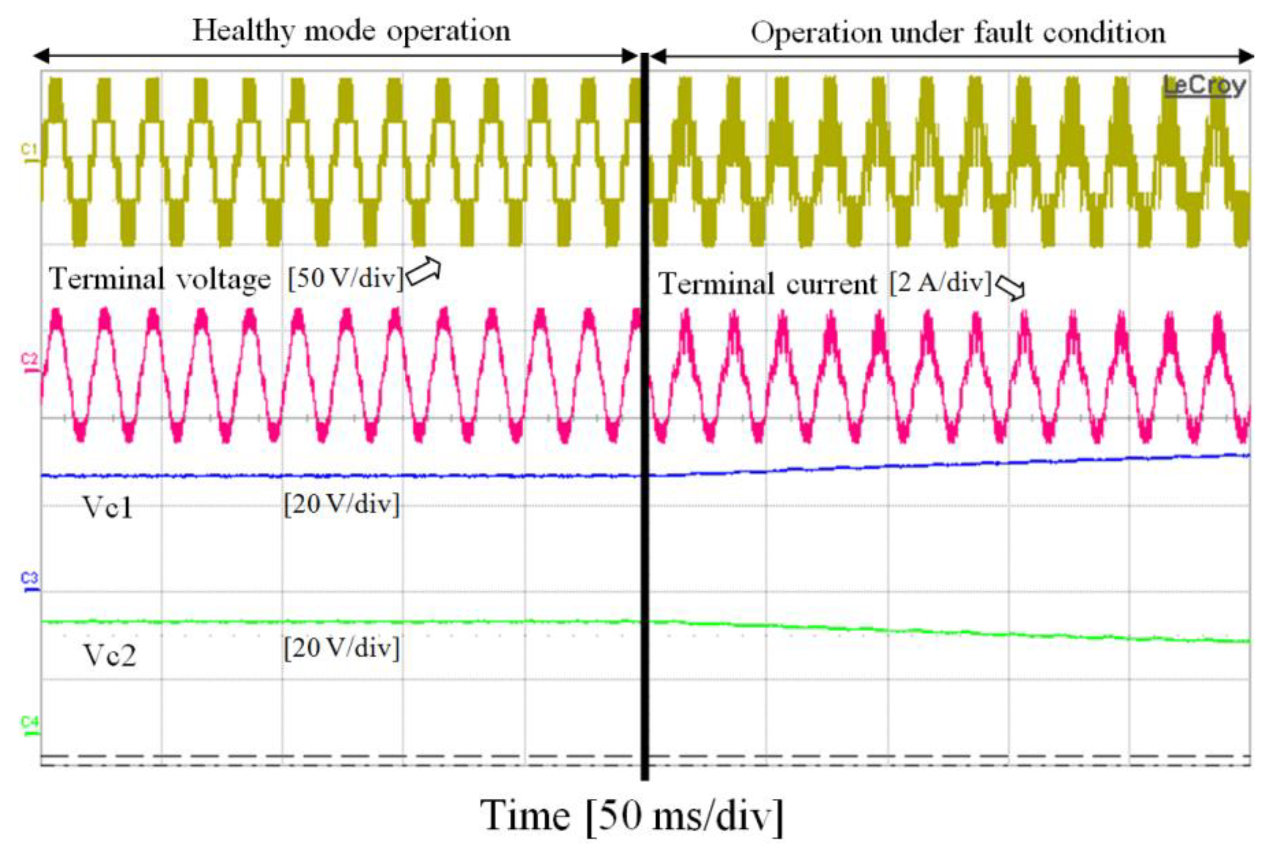
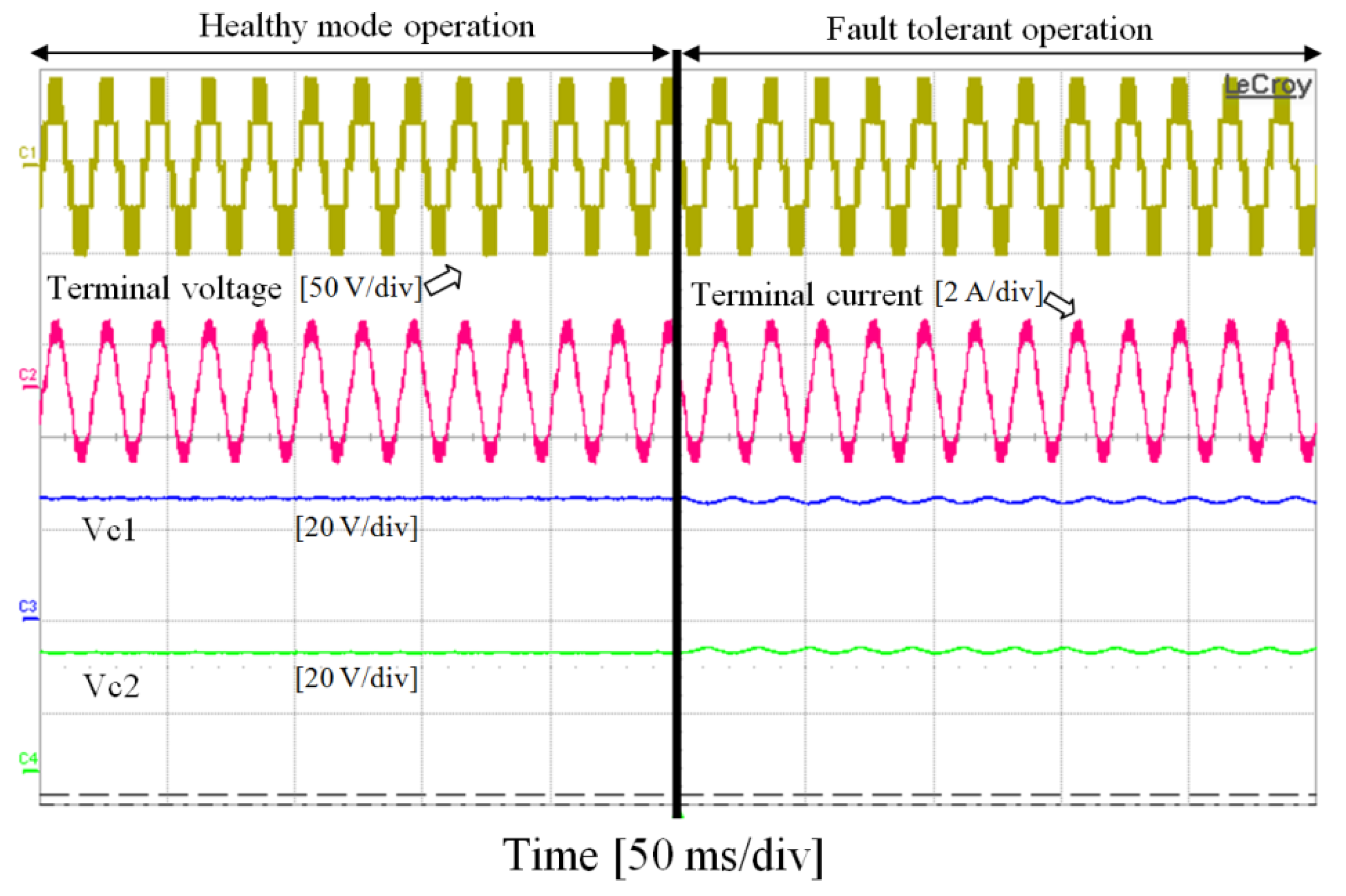
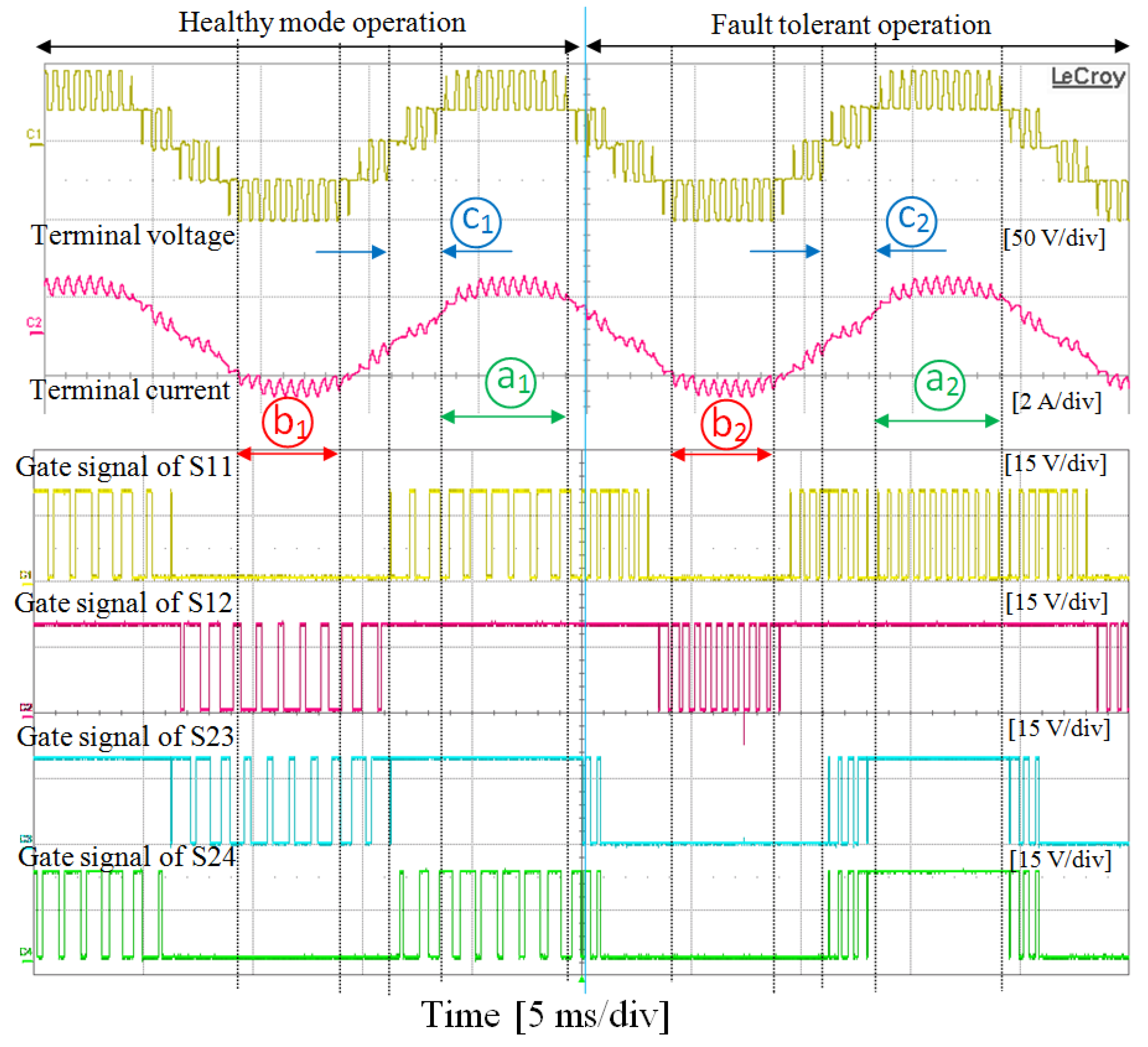
5. Experimental Results

To implement the presented algorithms and approaches, a dSPACE platform (MicroLabBox) including a Xilinx FPGA chip was employed. Since the fault diagnosis and modifications of the switching states during post-fault operation should be performed quickly, these operations were implemented on the FPGA module of the dSPACE. The employed converter comprises IGBTs with the reference number of SKM50GB123D (fabricated by SEMIKRON), commanded by SKHI22A drivers. The test bench employed is given in Figure 7. The same parameters pointed out in the simulation subsection were used on the employed test bench.
To create the failure in the clamping diodes, an auxiliary IGBT was used. To generate the open-circuit fault in the clamping diode, the auxiliary IGBT, connected in series with the relevant clamping diode and constantly closed in healthy conditions, was switched off. In the experimental results, the four gate signals applied to the power switches represent the switching pattern. In accordance with Table 2 and the four represented gate signals and based on the fact that the other four gate signals are complementary, each switching state can be estimated. Moreover, similar to the simulation section, clamping diode DC4 was considered as the faulty component.
In Figure 8, before the fault occurrence in DC4, the converter is in healthy conditions (interval 1). In this case, switching state 2 is applied, and the output voltage attains +Vdc/2 (in accordance with Table 2), and after the instant ta, the applied switching state and the output voltage are 5 and 0 V, respectively. The open-circuit failure is created in DC4 at the instant tb, and then the output voltage attains −Vdc/2. At tc, the counter starts and reaches the upper limit value. The failure is detected at td, but it is still not possible to identify the faulty component among S12, DC1, S23, and DC4. Thus, the second step is necessary, by switching on S11 according to Table 3. Thus, S11 is switched on at instant td, and the output voltage takes 0 V. However, after the execution of the second step, the defective component is still not distinguished between components S23 and DC4. Thus, performing the third step is necessary. For this purpose, at instant te, S24 is switched on, and the output voltage reaches +Vdc. Hence, at instant tf, DC4 is located as faulty. It should be mentioned that intervals 3 and 4 are considered to avoid any misdiagnosis because of dead times, delays, and transition times. The experimental results regarding the fault tolerant operation are represented in Figure 9, Figure 10 and Figure 11. Since the results presented in Figure 9, Figure 10 and Figure 11 are almost identical to Figure 4, Figure 5 and Figure 6, respectively, any repetitive explanation is avoided in this section. The detailed analysis and explanations are presented and discussed earlier.
It is important to mention that the case of a faulty clamping diode has been rarely studied in the literature; most of the time, it is assumed that these diodes never break down. Compared with the literature, this work proposes an original contribution to perform the continuity of service of five-level neutral-point-clamped inverters under clamping diode open-circuit failure, concerning two main aspects. First, regarding the fault diagnosis (detection and localization), we propose a logic-based method that does not require extra sensors or complicated calculations or modeling. Secondly, to perform fault-tolerant operation, no additional components are required, and the post-fault operation is realized at rated power, with the terminal current and voltage being the same before and after the fault occurrence. Table 7 summarizes the drawbacks of the conducted research compared with our contribution.

6. Conclusions

We have proposed a fast and efficient fault-tolerant method for clamping diodes of five-level NPC inverters. The fault diagnosis step does not require complicated calculations. Thus, it can be implemented on FPGA to achieve a high time performance. Moreover, it does not require any additional sensor, hardware, or component modeling. The diagnosis method is able to identify the faulty clamping diode. Following the fault diagnosis, this paper focuses on ensuring the continuity of service of the inverter in case of fault occurrence in clamping diodes. Secondly, the fault event in clamping diodes can cause the DC link capacitors to breakdown, and the fault event deteriorates the harmonic content of the terminal voltage and current. The proposed fault-tolerant approach is also realized without employing any redundant or additional components. Furthermore, during the post-fault operation, the rated current and voltage are achieved at the terminal. The simulation and experimental results are reported to validate the proposed strategy. As mentioned above, this paper presented fault diagnosis and fault-tolerant operation under an open-circuit fault event in clamping diodes, which has been rarely investigated. In summary, the proposed strategy can be applied in practice where an open-circuit fault occurs in a clamping diode, which is rarely taken into consideration in the already conducted research work.

Author Contributions

Investigation: S.A., P.P. and S.S.; Methodology: S.A., P.P. and S.S.; Supervision: P.P., S.S., and D.A.K.; Writing—original draft: S.A.; Writing—review and editing: P.P., D.A.K. and S.S. All authors have read and agreed to the published version of the manuscript.

Funding

This research work is the result of the collaboration between the University of Lorraine (France) and Iran University of Science and Technology (IUST) started in October 2018. It has been partially financially supported by the Scientific and Technologique Cooperation Service of the French Embassy in Tehran, and for this we express our thanks.

Conflicts of Interest

The authors declare no conflict of interest.

References

  1. Gautam, S.P.; Kumar, L.; Gupta, S.; Agrawal, N. A single-phase five-level inverter topology with switch fault-tolerance capabilities. IEEE Trans. Ind. Electron. 2017, 64, 2004–2014. [Google Scholar] [CrossRef]
  2. Rodriguez, J.; Lai, J.S.; Peng, F.Z. Multilevel inverters: A survey of topologies, controls, and applications. IEEE Trans. Ind. Electron. 2002, 49, 724–738. [Google Scholar] [CrossRef] [Green Version]
  3. Wu, B. High-Power Converters AC Drives; Wiley: Hoboken, NJ, USA, 2006. [Google Scholar]
  4. Lee, J.; Lee, K. Open-switch fault tolerance control for three-level NPC/T-Type rectifier in wind turbine systems. IEEE Trans. Ind. Electron. 2015, 62, 1012–1021. [Google Scholar] [CrossRef]
  5. Lee, J.; Lee, K. Open-circuit fault-tolerant control for outer switches of three-level rectifier in wind turbine systems. IEEE Trans. Power Electron. 2016, 31, 3806–3815. [Google Scholar] [CrossRef]
  6. Ceballos, S.; Pou, J.; Zaragoza, J.; Robles, E.; Villate, J.L.; Martin, J.L. Fault-tolerant neutral-point-clamped converter solutions based on including a fourth resonant leg. IEEE Trans. Ind. Electron. 2011, 58, 2293–2303. [Google Scholar] [CrossRef]
  7. Ceballos, S.; Pou, J.; Robles, E.; Gabiola, I.; Zaragoza, J.; Villate, J.L.; Boroyevich, D. Three-level converter topologies with switch breakdown fault-tolerance capability. IEEE Trans. Ind. Electron. 2008, 55, 982–995. [Google Scholar] [CrossRef]
  8. Rao, M.; Sivakumar, K. A fault-tolerant single phase five-level inverter for grid independent PV systems. IEEE Trans. Ind. Electron. 2015, 62, 7569–7577. [Google Scholar]
  9. Choi, U.; Lee, J.; Blaabjerge, F.; Lee, K. Open-circuit fault diagnosis and fault-tolerant control for a grid-connected npc inverter. IEEE Trans. Power Electron. 2016, 31, 7234–7247. [Google Scholar] [CrossRef]
  10. Li, S.; Xu, L. Strategies of fault tolerant operation for three-level PWM inverters. IEEE Trans. Power Electron. 2006, 21, 933–940. [Google Scholar] [CrossRef]
  11. Ceballos, S.; Pou, J.; Robles, E.; Zaragoza, J.; Martin, J.L. Performance evaluation of fault-tolerant neutral-point-clamped converters. IEEE Trans. Ind. Electron. 2010, 57, 2709–2718. [Google Scholar] [CrossRef]
  12. Abadi, M.B.; Mendes, A.M.S.; Cruz, S.M.A. Three-level NPC inverter fault diagnosis by the average current Park’s vector approach. In Proceedings of the 20th ICEM, Marseille, France, 2–5 September 2012; pp. 1893–1898. [Google Scholar]
  13. Mendes, A.M.S.; Abadi, M.B.; Cruz, S.M.A. Fault diagnosis algorithm for three-level neutral point clamped AC motor drives based on average current Park’s vector. IET Power Electron. 2014, 7, 1127–1137. [Google Scholar] [CrossRef]
  14. Lee, J.S.; Lee, K.B.; Blaabjerg, F. Open-switch fault detection method of a back-to-back converter using NPC topology for wind turbine systems. IEEE Trans. Ind. Appl. 2015, 50, 325–335. [Google Scholar] [CrossRef]
  15. Kim, T.J.; Lee, W.C.; Hyun, D.S. Detection method for open circuit fault in neutral-point-clamped inverter systems. IEEE Trans. Ind. Electron. 2009, 56, 2754–2763. [Google Scholar]
  16. Caseiro, L.M.A.; Mendes, A.M.S. Real-time IGBT open-circuit fault diagnosis in three-level neutral-point-clamped voltage-source rectifiers based on instant voltage error. IEEE Trans. Ind. Electron. 2015, 62, 1669–1678. [Google Scholar] [CrossRef]
  17. Choi, U.M.; Jeong, H.G.; Lee, K.B.; Blaabjerg, F. Method for detecting an open-switch fault in a grid-connected NPC inverter system. IEEE Trans. Power Electron. 2012, 27, 2726–2739. [Google Scholar] [CrossRef]
  18. Fazio, P.; Maragliano, G.; Marchesoni, M.; Parodi, G. A new fault detection method for NPC converters. In Proceedings of the 14th European Conference on Power Electronics and Applications, Birmingham, UK, 30 August–1 September 2011; pp. 1–10. [Google Scholar]
  19. Mendes, A.M.S.; Abadi, M.B.; Cruz, S.M.A. Method to diagnose open-circuit faults in active power switches and clamp-diodes of three-level neutral-point clamped inverters. IET Elect. Power Appl. 2016, 10, 623–632. [Google Scholar]
  20. Ge, X.; Pu, J.; Geo, B.; Liu, Y. An open-circuit fault diagnosis approach for single-phase three-level neutral-point-clamped converters. IEEE Trans. Power Electron. 2018, 33, 2559–2570. [Google Scholar] [CrossRef]
  21. Abari, I.; Lahouar, A.; Hamouda, M.; Slama, J.B.H.; Al-Haddad, K. Fault detection methods for three-Level NPC inverter based on DC-bus electromagnetic signatures. IEEE Trans. Ind. Electron. 2018, 65, 5224–5236. [Google Scholar] [CrossRef]
  22. Shahbazi, M.; Poure, P.; Saadate, S.; Zolghadri, M.R. Fault-tolerant five-level converter topology with FPGA-based reconfigurable control. IEEE Trans. Ind. Electron. 2013, 60, 2284–2294. [Google Scholar] [CrossRef] [Green Version]
Figure 1. Scheme of (a) a three-phase five-level NPC/H-bridge inverter and (b) a single-phase five-level NPC inverter.
Electronics 11 01461 g001
Figure 2. Proposed fault detection principle.
Electronics 11 01461 g002
Figure 3. Simulation results for localization of faulty clamping diode DC4 in the third step.
Electronics 11 01461 g003
Figure 4. Simulation results of the inverter operation under open-circuit fault occurrence in DC4, without fault-tolerant control.
Electronics 11 01461 g004
Figure 5. Simulation results for fault-tolerant operation of the inverter in case of fault occurrence in DC4.
Electronics 11 01461 g005
Figure 6. Detailed representation of the fault-tolerant operation in case of open-circuit fault occurrence in DC4.
Electronics 11 01461 g006
Figure 7. Experimental test bench.
Electronics 11 01461 g007
Figure 8. Experimental results for localization of faulty clamping diode DC4 in the third step.
Electronics 11 01461 g008
Figure 9. Experimental results of the inverter operation under fault condition without fault-tolerant control.
Electronics 11 01461 g009
Figure 10. Experimental results of the inverter operation with fault-tolerant control.
Electronics 11 01461 g010
Figure 11. Detailed experimental results of the fault-tolerant strategy.
Electronics 11 01461 g011
Table 1. Passing components corresponding to each switching state for positive and negative output currents in healthy operation.
Switching StateTerminal
Voltage
Conducting
Components (I > 0)
Conducting
Components (I < 0)
1+VdcS11, S12, S23, S24D11, D12, D23, D24
2+Vdc/2S11, S12, S23, DC4D11, D12, S22, DC3
3+Vdc/2DC1, S12, S23, S24DC2, S13, D23, D24
40S11, S12, D22, D21D11, D12, S21, S22
50DC1, S12, S23, DC4DC2, S13, S22, DC3
60D14, D13, S23, S24S13, S14, D24, D23
7−Vdc/2DC1, S12, D22, D21DC2, S13, S22, S21
8−Vdc/2D14, D13, S23, DC4S13, S14, DC3, S22
9−VdcD14, D13, D22, D21S13, S14, S22, S21
Table 2. Switching patterns corresponding to each voltage level.
Switching StateTerminal VoltageS11S12S13S14S21S22S23S24Attributed Decimal Number
1+Vdc11000011195
2+Vdc/211000110198
3+Vdc/20110001199
4011001100204
5001100110102
600011001151
7−Vdc/201101100108
8−Vdc/20011011054
9−Vdc0011110060
Table 3. Identification of the defective component for positive current.
StateFaulty Switch or DiodeConducting Components (Terminal Voltage)Second StepConducting Components (Terminal Voltage)
1S11DC1, S12, S23, S24 (Vdc/2)S24 is switched offDC1, S12, S23, DC4 (0)
1S24S11, S12, S23, DC4 (Vdc/2)S11, S12, S23, DC4 (Vdc/2)
1S12D14, D13, S23, S24 (0)S23 is switched offD14, D13, D22, D21 (−Vdc)
1S23S11, S12, D22, D21 (0)S11, S12, D22, D21 (0)
2S12D14, D13, S23, DC4 (−Vdc/2)S12 is identified in the first step.
2S11DC1, S12, S23, DC4 (0)S24 is switched onDC1, S12, S23, S24 (Vdc/2)
2S23S11, S12, D22, D21 (0)S11, S12, D22, D21 (0)
2DC4S11, S12, D22, D21 (0)S11, S12, S23, S24 (Vdc)
3S23DC1, S12, D22, D21 (−Vdc/2)S23 is identified in the first step.
3S12D14, D13, S23, S24 (0)S11 is switched onD14, D13, S23, S24 (0)
3DC1D14, D13, S23, S24 (0)S11, S12, S23, S24 (Vdc)
3S24DC1, S12, S23, DC4 (0)S11, S12, S23, DC4 (Vdc/2)
5S12D14, D13, S23, DC4 (−Vdc/2)S11 is switched onD14, D13, S23, DC4 (−Vdc/2)
5DC1D14, D13, S23, DC4 (−Vdc/2)S11, S12, S23, DC4 (Vdc/2)
5S23DC1, S12, D22, D21 (−Vdc/2)S11, S12, D22, D21 (0)
(see Table 5 for third step)
5DC4DC1, S12, D22, D21 (−Vdc/2)S11, S12, D22, D21 (0)
(see Table 5 for third step)
7S12D14, D13, D22, D21 (−Vdc)S11 is switched onD14, D13, D22, D21 (−Vdc)
7DC1D14, D13, D22, D21 (−Vdc)S11, S12, D22, D21 (0)
8S23D14, D13, D22, D21 (−Vdc)S24 is switched onD14, D13, D22, D21 (−Vdc)
8DC4D14, D13, D22, D21 (−Vdc)D14, D13, S23, S24 (0)
Table 4. Identification of the defective component in the third step.
StateFaulty Switch or DiodeThird StepConducting Components (Terminal Voltage)
5,
(I > 0)
S23S24 is switched onS11, S12, D22, D21 (0)
5,
(I > 0)
DC4S11, S12, S23, S24 (Vdc)
5,
(I < 0)
S22S21 is switched onS13, S14, D23, D24 (0)
5,
(I < 0)
DC3S13, S14, S21, S22 (−Vdc)
Table 5. Modification of the switching states to acquire fault-tolerant operation.
Faulty Clamping DiodeInfeasible Switching StateSubstituted Switching State
DC132
54 or 6
78
DC232
54 or 6
78
DC323
54 or 6
87
DC423
54 or 6
87
Table 6. Simulation parameters associated with their values.
ParametersValues
Load resistance27.7 Ω
Load inductance9 mH
DC link voltage50 V
DC link capacitor2.2 mF
Switching frequency1 kHz
Modulation index0.8
Table 7. Drawbacks of the conducted research work compared with this paper.
ReferencesDrawback
[1,4,5,6,7,8]Are not able to ensure fault-tolerant operation in case of fault event in a clamping diode
[9,11]Output voltage THD increases during post-fault operation
[10]The rated voltage is not restored during post-fault operation
[12,18]Are not able to locate a defective clamping diode
[19]Extra sensors are required for fault diagnosis
[20]Knowing the grid parameters is required for fault diagnosis
[21]External antennas and filters are required for fault diagnosis
Publisher’s Note: MDPI stays neutral with regard to jurisdictional claims in published maps and institutional affiliations.

