Article

3D Heterogenous Integrated Wideband Switchable Bandpass Filter Bank for Millimeter Wave Applications

1
School of Aeronautics and Astronautics, Zhejiang University, Hangzhou 310027, China
2
China International Engineering Consulting Corporation, Beijing 100048, China
3
Zhejiang Chengchang Technology Co., Ltd., Hangzhou 310030, China
*
Author to whom correspondence should be addressed.
Electronics 2023, 12(1), 194; https://doi.org/10.3390/electronics12010194
Submission received: 11 November 2022 / Revised: 22 December 2022 / Accepted: 26 December 2022 / Published: 30 December 2022
(This article belongs to the Section Semiconductor Devices)

Abstract

:
This article proposes a three-dimensional heterogenous-integrated (3DHI) switchable bandpass filter bank with two independent wideband filter channels that cover 26–40 GHz and 32.5–40 GHz, respectively. An accurate wafer-level process with a high hollowed ratio of the applied 8-inch high-resistivity-silicon (HR-Si) interposer wafers is presented to form both compact filter channels. Above the interdigital filter patterns fabricated on the bottom interposer wafer, deep cavities are etched in the cap interposer wafer to improve the quality factor of the filter bank. Besides the cavities, the cap interposer wafer is 35% hollow inside, which two bare dies of GaAs single-pole double-throw (SPDT) switches and two thin film resistors are attached to the bottom interposer after the wafer-to-wafer (W2W) bonding. To ensure good out-of-band performance, a 3D EM co-simulation of the switch layout at the chip level and filter patterns at the package level is applied. Measurement results show that the switchable filter bank achieves a high isolation of 50 dB and a competitive shape factor (BW30dB/BW3dB) of about 1.3. In addition, the size of the switchable filter bank is only 7.0 mm × 3.5 mm × 0.6 mm, and the weight is only 0.1 g.

1. Introduction

With the increasing trend of multiband and reconfigurability in modern microwave communication systems, switchable filter banks have attracted more and more attention. Commonly, switchable filter banks are designed in planar technology employing PIN diodes, FETs, microelectromechanical systems (MEMS) switches, and varactors [1,2]. To meet the requirement of high performance in wideband applications, more filter channels are integrated into one switchable filter bank module, which increases the module complexity and the package size of systems.
To address the above challenging issues, researchers focus on exploring different fabrication processes to improve the integration and compactness, including multilayer printed circuit board (PCB) [3,4,5], low temperature cofired ceramic (LTCC) [6,7], silicon wafer [8,9,10,11], and other materials [12]. Multilayer PCB is often considered a low-cost technology, but it still suffers from the low integration density of electronic systems and low isolation. LTCC shows remarkable RF performance, which has a minimal loss at microwave and high integration but provides limited quality factor. Advanced silicon-based processes are to achieve compact size, excellent quality factor, and adequate isolation. Therefore, the 3DHI process with HR-Si is promising to achieve these extraordinary performances.
In previous 3DHI switchable filter bank designs [8,9,10,11], switch chips are commonly embedded inside the HR-Si interposer cavities before interposer stacking. In addition, these works show good performances with multiple adjacent frequency bands and narrow band overlaps, which are mainly operated at several specific frequencies for active detection or known communication missions. However, for applications such as passive reconnaissance receivers, real-time passive detections of unknown ultra-wideband signals are performed. For regular filter banks with multiple adjacent bands, due to the band discontinuity, unknown vital signals in one band might be missed when the filter bank is shifting among other bands. Therefore, an ultra-wideband preselect filter channel is preferred with a large instantaneous bandwidth.
In this article, a generalized design of a 3DHI switchable bandpass filter bank for the passive detection of Ka band unknown signals is proposed with high integration, high isolation, and high shape factors. Two compact wideband filter channels with large band overlap are integrated by two stacked HR-Si interposer wafers, one of which covers an ultra-wideband of 26–40 GHz for around-the-clock spectrum surveillance and the other one covers a relatively narrow band of 32.5–40 GHz for vital radar signal reconnaissance with a large signal-to-clutter ratio. To approach high efficiency, low cost, and high process consistency, a wafer-level process adapted to a 35% hollowed 8-inch interposer wafer is presented, which is compatible with the following switch chip embedding process. To achieve high channel isolation, a 3D co-simulation of the switch layout at the chip level and filter patterns at the package level are presented.
The organization of this article is discussed as follows: In Section 2, a detailed design procedure and simulation results of the switchable filter bank are proposed. Subsequently, Section 3 illustrates the fabrication process. Section 4 presents measured results and the discussion. Section 5 concludes this article.

2. Design of Switchable Filter Bank

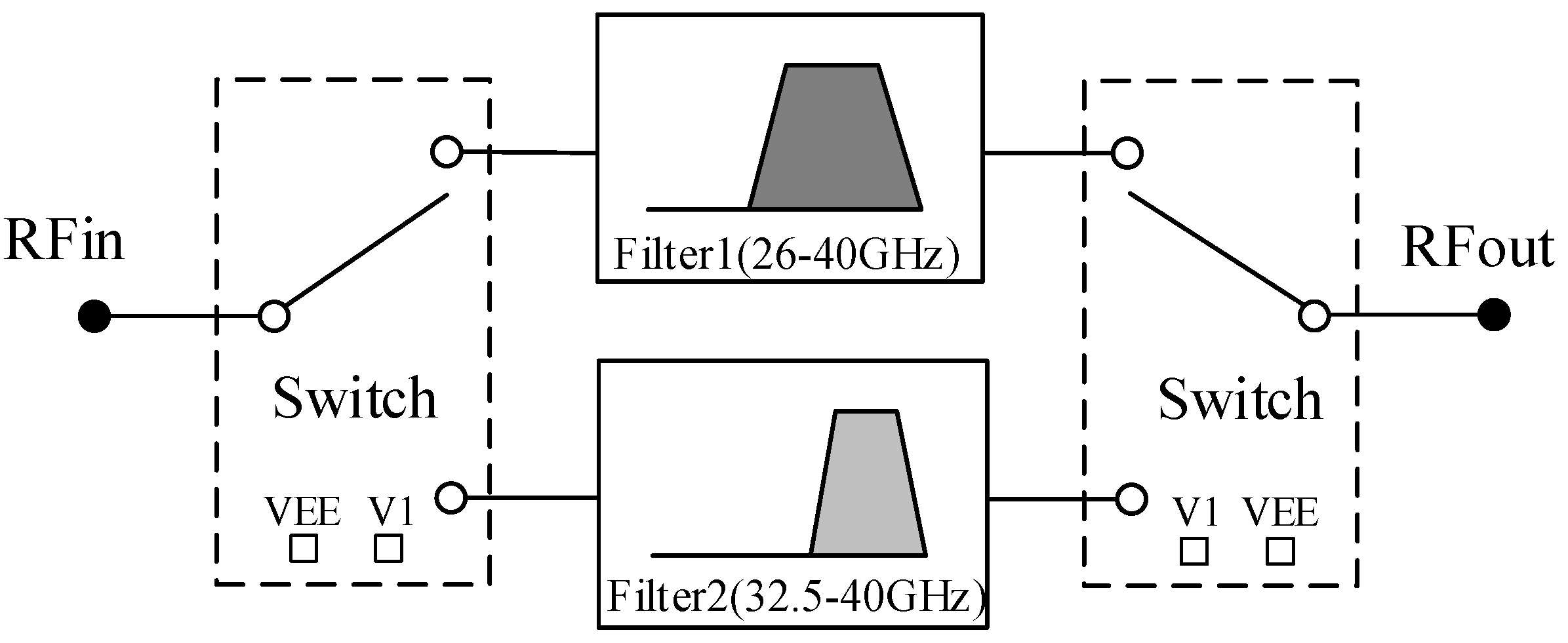
2.1. System Architecture

The proposed switchable filter bank consists of two SPDT switches and two bandpass filters (BPFs), as shown in Figure 1. For the SPDT switch, VEE is the −5 V DC supply pad, and V1 is the control signal pad, which selects two different filter channels with a TTL logic level of “0” (0 V) or “1” (5 V). When the state is “1”, filter channel 1 (26–40 GHz) is turned on. In this operating mode, the switchable filter bank works as an ultra-wideband preselect filter for around-the-clock spectrum surveillance with a 14 GHz instantaneous bandwidth. On one hand, the ultra-wideband covers most near-Earth communication bands (from 26–32.5 GHz), such as Starlink of the US [13] and Star Network of China [14], and on the other hand, it covers most Ka band radar spectrum (from 32.5–40 GHz) [15]. To improve the signal-to-clutter ratio of weak spectrum signals, filter channel 2 with a narrower bandwidth (32.5–40 GHz) is selected by changing the logic level to “0” for more important radar signal reconnaissance [16,17]. Within the limited filter bank dimensions, only the two filter channels mentioned above are integrated.

2.2. Bandpass Filter Design

Since typical unshielded or half-shielded resonators such as microstrip resonators have low-quality factors and inevitable channel crosstalk, this article employs two-layer HR-Si interposers with TSV fences and metal layers to create electromagnetic shielding and increase the quality factor of the filter bank, as shown in Figure 2. Above the metal filter patterns fabricated on the 200 μm-thick bottom interposer wafer, 200 μm-deep cavities are etched in the 300 μm-thick cap interposer wafer to further improve the quality factors. Due to the advantages of a compact structure and a wide range of design parameters, a short-circuited quarter-wavelength interdigital filter topology is used to design both filter channels [18,19]. Considering the tradeoff between the high shape factor and compact size of the filters, the Chebyshev lowpass prototype filter is selected for both filters with the filter order n = 13, and the element values g j can be obtained. The coupling coefficient k j , j + 1 and the external quality factor Q of the filter can be calculated using the following equations [20]:
k j , j + 1 = F B W g j g j + 1
Q e 1 = g 0 g 1 F B W       Q e n = g n g n + 1 F B W
where FBW is the fractional bandwidth of the designed filter.
After deducing the initial physical parameters for the interdigital bandpass filter, including the coupling space and the widths and lengths of resonators, the filter structure is modeled and optimized using HFSS. By adjusting the widths of the 1st and 13th resonators and the tap-in positions, terminal matching is improved to achieve ultrawide operational bandwidths. The optimized geometry parameters shown in Figure 2 include: w1 = 0.2 mm, w2 = 0.154 mm, w3 = 0.15 mm, w4 = 0.154 mm, l1 = 0.809 mm, l2 = 0.711 mm, l3 = 0.761 mm, l4 = 0.663 mm, s1 = 0.039 mm, s2 = 0.061 mm, s3 = 0.066 mm, s4 = 0.069 mm, s5 = 0.07 mm, s6 = 0.071 mm, s7 = 0.073 mm, s8 = 0.126 mm, s9 = 0.136 mm, s10 = 0.146 mm, s11 = 0.151 mm, and s12 = 0.151 mm.
Figure 3 shows the simulation results of bandpass filter channel 1 (26–40 GHz) and bandpass filter channel 2 (32.5–40 GHz). For filter channel 1, the insertion loss is less than 2.6 dB at 33 GHz, the return loss in the passband is higher than 10 dB, and the stopband rejection is greater than 40 dBc at the frequency range below 22 GHz and above 43 GHz. For filter channel 2, the insertion loss is less than 4.1 dB at 36 GHz, the return loss in the passband is higher than 10 dB, and the stopband rejection is greater than 40 dBc at the frequency range below 28 GHz and above 43 GHz.

2.3. Codesign of Filter and Switch

The constructure of the switchable filter bank is shown in Figure 4. Two bare dies of GaAs SPDT switches are mounted on the bottom interposer within the hollowed region of the cap interposer. For channel selection in this design, a GaAs pHEMT switch (G7803, Zhejiang Chengchang Technology, Hangzhou, China) is utilized. It shows a typical insertion loss of 1.5 dB, a low switching time of less than 20 ns, and an isolation of around 35 dB.
Switches and filter channels are connected through wire bonding. Considering the increasing parasitic coupling and crosstalk in the millimeter wave band, when co-designing the switchable filter bank, it is necessary to consider the isolation degradation between input and output terminals and between the two filter channels.
Commonly, in order to obtain the performance of a filter bank, S-parameters from both the circuit simulation of the switch chip and the EM simulation of the filter channels are achieved, and then the cascaded S-parameters are calculated. However, in this design, the control signal pads of the two SPDT switches are connected, which may cause weak crosstalk between the two RF terminals through the control signal line. Considering the high out-of-band rejection requirement of this work, crosstalks located in the rejection bands are unacceptable. Therefore, to ensure good out-of-band performance, a 3D EM co-simulation of the switch layout at the chip level and filter patterns at the package level is applied. For simplification, active transistors in switch chips are treated as short to ground for the “Off” state and open to ground for the “On” state. Weak but non-negligible crosstalk is found at 48 GHz when filter channel 2 (32.5–40 GHz) is selected. The E-field distribution of the crosstalk by the 3D EM co-simulation is shown in Figure 5a. To better show the path of the weak crosstalk, the color bar of the E-field is limited to 1 × 10⁵ V/m. To alleviate the crosstalk between the input and output terminals of the filter bank, two 100 Ω thin film resistors are implemented in series between the V1 pads of each switch.
Figure 6 illustrates the switchable filter bank’s simulation results with and without the resistors. It can be observed that the stopband rejection has improved from 30 dBc to 45 dBc. Although grounded TSV fences are set between the two filter channels to achieve a high level of channel isolation, slight RF signal leakage still exists through the two SPDT switches. Especially when filter channel 2 (32.5–40 GHz) is turned on, RF crosstalk exists through switches and filter channel 1 (26–40 GHz). As a result, stopband rejection ranging from 26 to 32.5 GHz in channel 2 degrades and can be treated as channel isolation for the switchable filter bank. Figure 6 shows that up to 60 dB of channel isolation can be achieved.

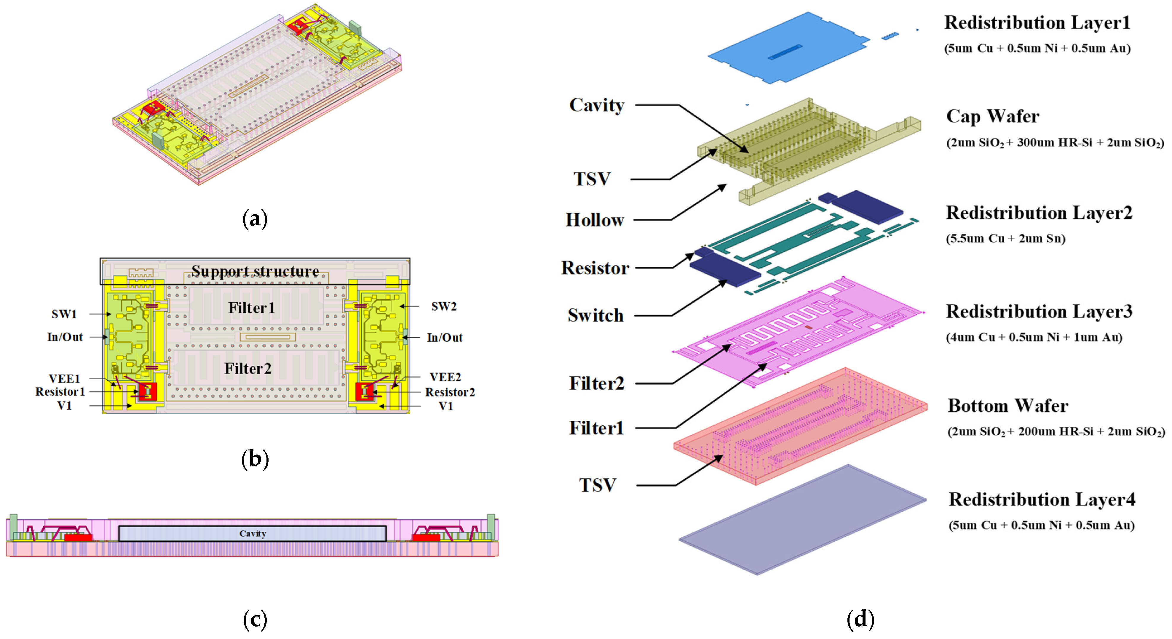
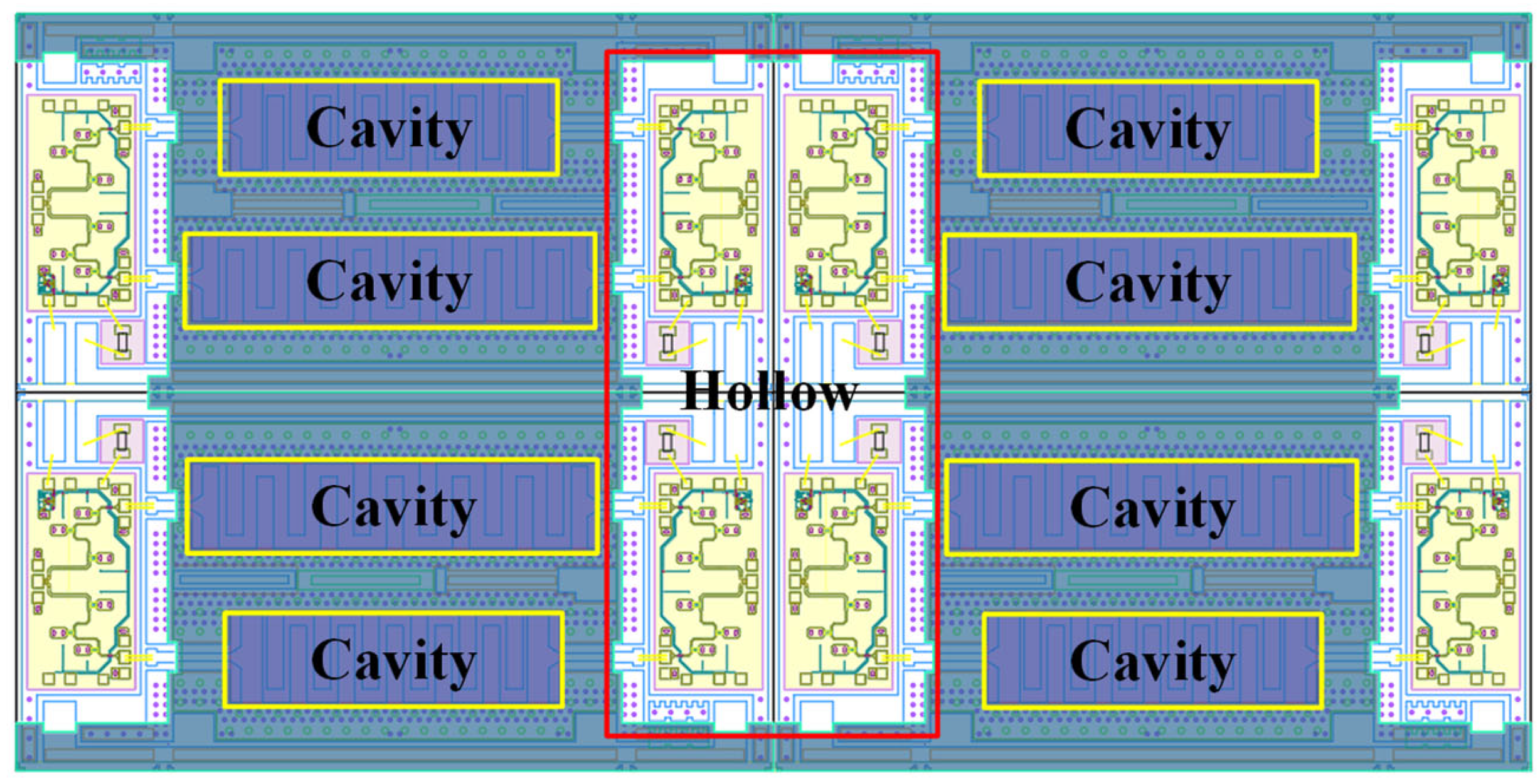
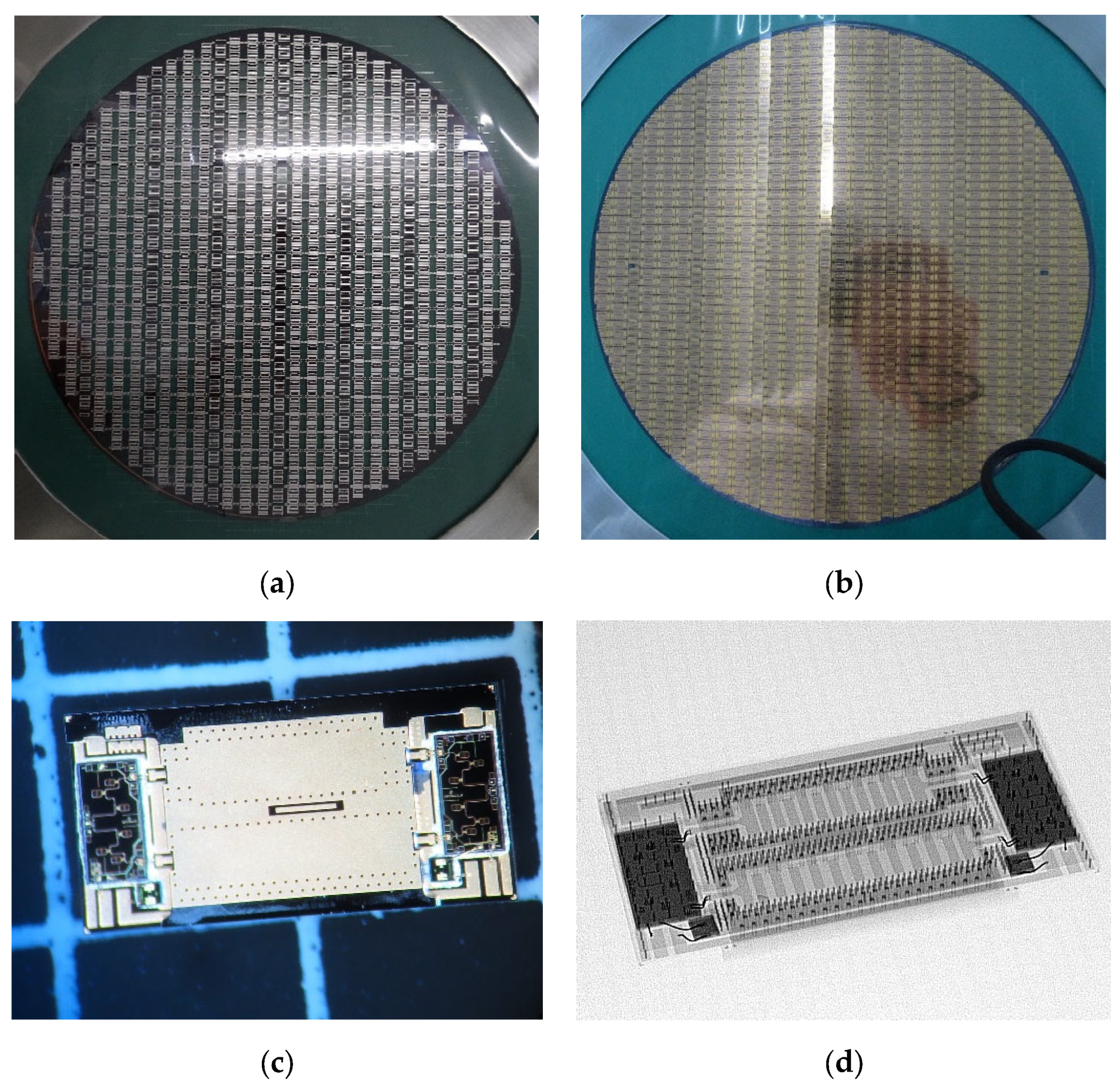
3. Fabrication Using Wafer-Level 3DHI

To realize the above two-layer interposer design with a high-efficiency, low-cost, and high-consistency wafer-level process, the following 3DHI process adapted to a 35% hollowed 8-inch interposer wafer is presented, which is compatible with the followed switch chip embedding process. The distribution map of the hollowed regions and cavities on the wafer is shown in Figure 7. The process of each interposer wafer and the assembly of the two-layer interposer structure will be discussed below in detail.

3.1. Cap Interposer Wafer

Figure 8 shows the main fabrication process steps for the cap interposer. At first, a 677 μm HR-Si wafer with a resistivity of around 3000 Ω·cm is given. A lithography step is performed using a positive-tone photoresist to specify the location of the TSVs. After lithography, φ60 μm × 300 μm TSV is formed on the wafer by a deep reactive ion etching (DRIE) process based on a modified BOSCH process [21]. Then, TSVs are deposited with a 2 μm SiO2 layer and followed by physical vapor deposition (PVD) sputtering to give nominal thicknesses of 0.5 μm Ti and 3 μm Cu, which work as a barrier/seed layer. In the next step, TSVs are filled by combing the conformal electroplating process and the bottom-up electroplating process. To level the copper filling with the surrounding wafer surface, Cu and Ti are removed with chemical-mechanical polishing (CMP). After the TSV formation, the Cu re-distributed layer (RDL) is finished using the Ni/Cu/Au electroplating process. After the front-side processing of the interposer wafers is completed, a support wafer is bonded using temporary adhesive bonding. The silicon must be ground to the remaining thickness of the TSV depth so that the backside of the wafer can be reached.
In the following fabrication steps, the 200 μm-deep cavity is etched using DRIE from the reverse side. After oxide deposition, Cu RDL is completed using the Cu electroplating process. In addition, the most challenging part of this construction of the cap interposer is to form the 300 μm-deep hollow, which is 35% of the whole cap wafer. The hollowing etching process is similar to the cavity etching process, but the amount of photoresist in various places must be properly regulated. In addition, the photoresist on the bottom of cavities must be thick enough to avoid over-etching. At the end of the process, the cap interposer is finished with support wafer debonding and wafer cleaning.
Figure 8. Process flow of the cap interposer wafer.
Electronics 12 00194 g008

3.2. Bottom Interposer Wafer

The main fabrication steps for the bottom interposer are depicted in Figure 9. The Bosch process is applied to etch the φ30 μm × 200 μm TSVs. After TSVs are filled with Cu, the excess copper is fully removed, leaving the copper-filled blind holes’ surface flush with the wafer’s surface. Then, Cu RDL is finished by using the Ni/Cu/Au electroplating process. When the front-side processing of the interposer wafers is completed, temporary adhesive bonding is used to affix a support wafer. In the following fabrication steps, the same procedure is used to treat the opposite surface [22].

3.3. Interposer Wafer Stacking

Following the fabrication of the two interposers, the 35% hollowed cap interposer wafer is stacked onto the bottom interposer wafer to form the filter bank with the wafer-to-wafer (W2W) bonding process. The total thickness variation (TTV) of the wafer is a crucial indicator of W2W bonding, which is normally confined to 1 μm or less. In the fusion bonding procedure, Sn is initially heated to generate metal compounds with copper. The stability of the produced alloy heavily depends on the Sn layer thickness and bonding time. Certainly, the alloy is also impacted by the bonding temperature. With the low heating rate, the melting of Sn is incomplete, and the alloy layer bubbles. On the other hand, when the heating temperature is excessively high, it is simple for Sn to overflow. To avoid RF performance degradation, the offset of the two interposer wafers is controlled to be less than 5 μm.
After W2W bonding of the two interposers, two bare dies of SPDT switches are attached by utilizing conducting resin, as shown in Figure 10. Subsequently, wire bonding is employed as the interconnection between embedded bare dies and interposers. Additionally, the fabrication process is finished after wafer dicing. Compared to the design in [9], W2W bonding of the two interposers is conducted before switch chip embedding and wire bonding, which can effectively increase the product’s yield and reliability.

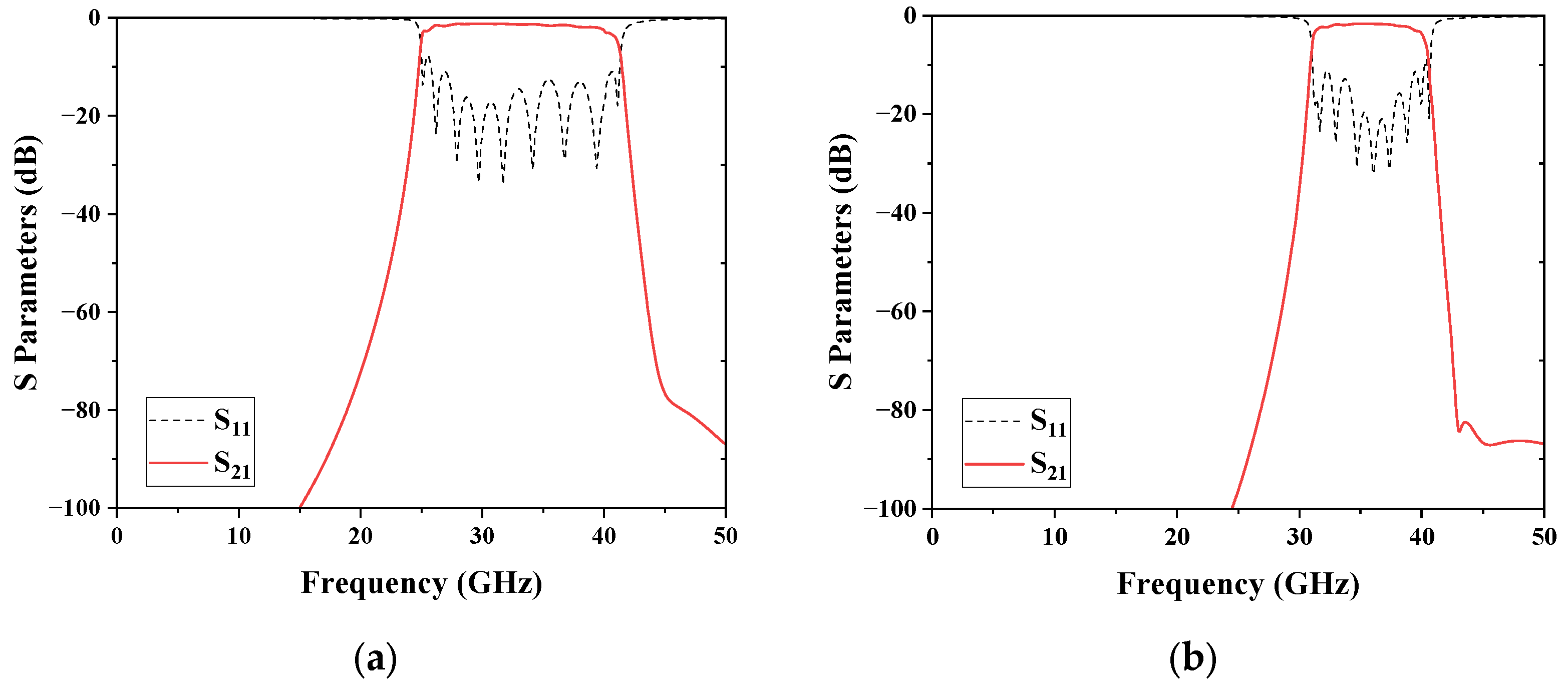
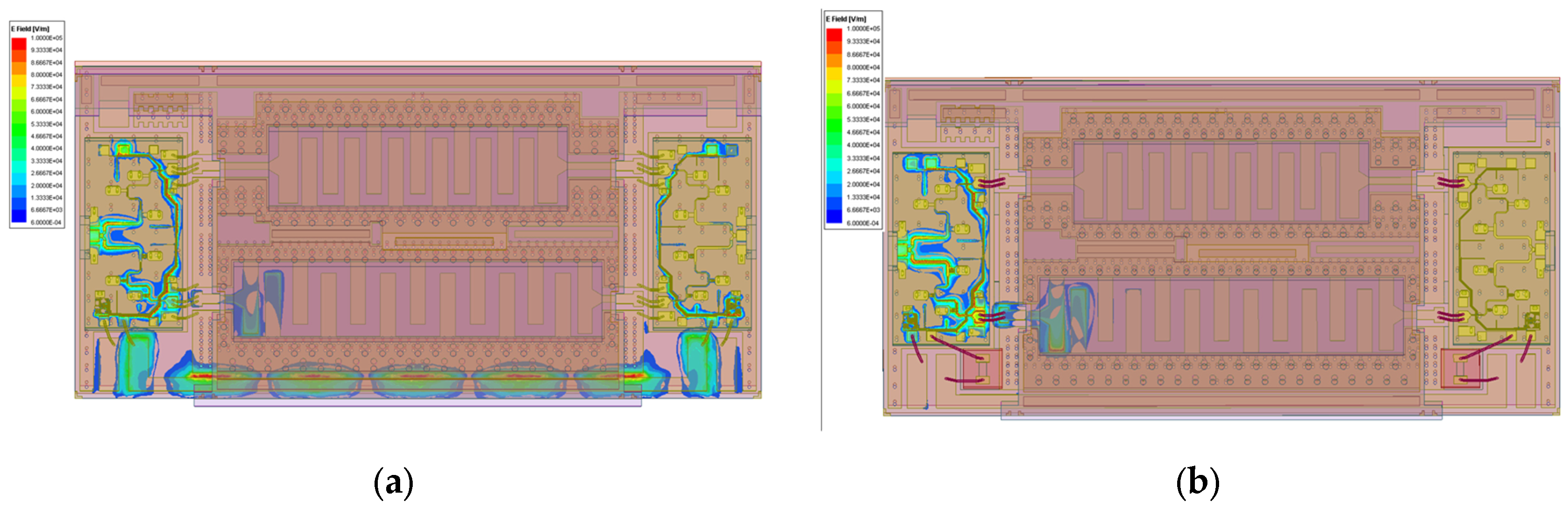
4. Measured Results and Discussion

Based on the above process, the switchable filter bank is fabricated. Figure 11a,b show the HR-Si cap and bottom interposer wafers. Figure 11c,d show the photo and the X-ray image of the switchable filter bank. The overall size is 7.00 mm × 3.50 mm × 0.60 mm, and the weight is 0.1 g.
The S-parameters of the switchable filter bank are measured using a semiconductor parameter analyzer (B1500A) and a vector network analyzer (N5247B) with 150-μm-pitch ground-signal–ground (GSG) RF probes. As shown in Figure 12, the test results of the two filter channels show that the passband return losses are both larger than 10 dB, which are in close agreement with the simulation results. The measured insertion losses are 4.8–6.9 dB for filter channel 1 (26–40 GHz) and 6.3–8.1 dB for filter channel 2 (32.5–40 GHz). The insertion loss degradation and frequency deviation are mostly attributed to nonideal material losses and fabrication tolerance. Based on our analysis, sparse SiO2 deposition by PECVD in the fabrication process is most likely the dominant factor for the insertion loss degradation and frequency deviation. To verify the issue, GCPW lines with different lengths fabricated on redistribution layers 3 and 4 are simulated and measured to fit the material parameters. When the optimized relative dielectric constant and loss tangent of the 2 μm-thick SiO2 layers are approaching 3 and 0.02, respectively, the best fitting is achieved. Furthermore, these corrected material parameters are applied to the simulation of the switchable filter bank. The simulated, modified, and measured results of the filter bank are shown in Figure 12. The modified simulation results are in close agreement with the measured ones. The stopband rejection of filter channel 2, which ranged from 26 GHz to 32.5 GHz, is treated as the channel isolation of the switchable filter bank, which is more than 50 dB. It is worth noting that the competitive shape factors (BW30dB/BW3dB) of the two filter channels are (43.1–24.1 GHz)/(40.7–25.7 GHz) = 1.27 and (42–31 GHz)/(40.5–32.2 GHz) = 1.33, respectively.
Table 1 summarizes the performance comparison to previous works on switchable filter banks. The designed filter bank in this article shows ultra-wide bandwidth and a competitively small shape factor in millimeter-wave with minimal compact size.

5. Conclusions

In this article, a switchable bandpass filter bank that covers 26–40 GHz and 32.5–40 GHz is designed and implemented with a 3DHI process. Compact wideband filter channels are integrated by two stacked HR-Si interposer wafers with cavities, TSV fences and metal layers to create electromagnetic shielding and increase the quality factor of the filter bank. A wafer-level process adapted to a 35% hollowed 8-inch interposer wafer is applied, which is compatible with the followed switch chip embedding process. The test results show good agreement with the simulation results and achieve a competitive shape factor of about 1.3. Assisted by the 3D co-simulation of switch layout at chip level and filter patterns at package level, more than 50 dB of isolated channels are measured. The provided fabrication process is promising for millimeter wave communication applications.

Author Contributions

Conceptualization, Z.W.; methodology, Z.W. and Y.S.; validation, S.M. and X.G.; formal analysis, Y.S. and X.D.; data curation, W.Y. and X.D.; writing, Z.W. and Y.S.; supervision, X.L. and F.Y. All authors have read and agreed to the published version of the manuscript.

Funding

This research received no external funding.

Data Availability Statement

Not applicable.

Acknowledgments

The authors would like to thank the Institute of Aerospace Electronics Engineering at Zhejiang University for providing the research platform and technical support.

Conflicts of Interest

The authors declare no conflict of interest.

References

  1. Chan, K.Y.; Ramer, R.; Mansour, R.R. A Switchable Iris Bandpass Filter Using RF MEMS Switchable Planar Resonators. IEEE Microw. Wirel. Compon. Lett. 2017, 27, 34–36. [Google Scholar] [CrossRef]
  2. Shojaei-Asanjan, D.; Mansour, R.R. The Sky’s the Limit: A Switchable RF-MEMS Filter Design for Wireless Avionics Intracommunication. IEEE Microw. Mag. 2017, 18, 100–106. [Google Scholar] [CrossRef]
  3. Ma, K.; Wang, Y.; Li, W.; Chen, Y. A Novel Compact Self-Packaged SPDT Switchable BPFs Based on SISL Platform. IEEE Trans. Ind. Electron. 2019, 66, 7239–7249. [Google Scholar] [CrossRef]
  4. Bohorquez, J.; Potelon, B.; Quendo, C.; Cariou, M.; Manchec, A.; Segalen, R.; Karpus, F.; Cadiou, S. Design of a Compact, Highly-Integrated, Eight-Filter Module Using Multilayered-PCB. In Proceedings of the 2021 IEEE MTT-S International Microwave Filter Workshop (IMFW), Perugia, Italy, 17–19 November 2021; pp. 192–194. [Google Scholar]
  5. Ma, K.; Jayasuriya, R.M.; Lim Chin Siong, D.R. Fully Integrated High-Isolation Low-Loss Digitally Controlled MEMS Filters. IEEE Trans. Ind. Electron. 2011, 58, 2690–2696. [Google Scholar] [CrossRef]
  6. Yang, X.; Xing, M.; Wang, E.; Zhang, L.; Li, N.; Qian, Z. A Design of S-Band Monolithic Integrated Switched Filter Bank. In Proceedings of the 2017 18th International Conference on Electronic Packaging Technology (ICEPT), Harbin, China, 16–19 August 2017; pp. 177–181. [Google Scholar]
  7. Yu, H.; Wang, X.; Zhang, L.; Niu, X.; Yi, L.; Deng, L.; Jiang, C. A LTCC-Based Wideband TR Module with Sub-Band BPFs for Active Phased Array System. In Proceedings of the 2019 IEEE MTT-S International Wireless Symposium (IWS), Guangzhou, China, 19–22 May 2019; pp. 1–3. [Google Scholar]
  8. Hou, F.; Sun, C.; Luan, H.; Huang, M.; Zhu, J.; Hu, S. Heterogeneously Integrated Compact Switchable Filters in 3D-MEMS Silicon Process for Millimeter Wave Application. Res. Prog. SSE 2021, 41, 330–336. [Google Scholar]
  9. Hou, F.; Shen, Y.; Luan, H.; Sun, C.; Huang, M.; Zhu, J.; Hu, S. Micropackaged Compact Switchable Filters With High Isolation in 3-D TSV-MEMS Process. IEEE Trans. Compon. Packag. Manuf. Technol. 2021, 11, 647–654. [Google Scholar] [CrossRef]
  10. Huang, M.; Wang, T.; Hou, F.; Su, P.; Sun, C.; Luan, H. A 3D TSV-MEMS Based Heterogeneous Integration Technology for RF Application. In Proceedings of the 2021 22nd International Conference on Electronic Packaging Technology (ICEPT), Xiamen, China, 11–14 August 2021; pp. 1–4. [Google Scholar]
  11. Hou, F.; Li, L.; Shen, Y.; Sun, C.; Luan, H.; Hu, S. Wideband Switchable Sharp-Rejection Filter in Compact 3-D Heterogeneous Integration. IEEE Trans. Compon. Packag. Manuf. Technol. 2022, 12, 1583–1590. [Google Scholar] [CrossRef]
  12. Chan, K.Y.E.; Ramer, R.; Guo, Y.J. RF MEMS Millimeter-Wave Switchable Bandpass Filter. In Proceedings of the 2013 IEEE International Wireless Symposium (IWS), Beijing, China, 14–18 April 2013; pp. 1–4. [Google Scholar]
  13. Pachler, N.; del Portillo, I.; Crawley, E.F.; Cameron, B.G. An Updated Comparison of Four Low Earth Orbit Satellite Constellation Systems to Provide Global Broadband. In Proceedings of the 2021 IEEE international conference on communications workshops (ICC workshops), Montreal, QC, Canada, 14–23 June 2021; IEEE: Piscataway, NJ, USA, 2021; pp. 1–7. [Google Scholar]
  14. Li, F.; Yu, H.; Ding, R.; Wang, N.; Wang, Y.; Zhou, Z. Development Strategy of Space Internet Constellation System in China. Chin. J. Eng. Sci. 2021, 23, 137. [Google Scholar] [CrossRef]
  15. Zhu, Y.; Zheng, Y.; Fang, S.; Zou, Y.; Pearson, S. Analysis of the Brightness Temperature Features of the Lunar Surface Using 37 GHz Channel Data from the Chang’E-2 Microwave Radiometer. Adv. Space Res. 2019, 63, 750–765. [Google Scholar] [CrossRef]
  16. Görsdorf, U.; Lehmann, V.; Bauer-Pfundstein, M.; Peters, G.; Vavriv, D.; Vinogradov, V.; Volkov, V. A 35-GHz Polarimetric Doppler Radar for Long-Term Observations of Cloud Parameters—Description of System and Data Processing. J. Atmos. Ocean. Technol. 2015, 32, 675–690. [Google Scholar] [CrossRef]
  17. Ludwig, M.; Daganzo-Eusebio, E.; Davidson, M. Ka-Band Radar Missions for Earth Observation. In Proceedings of the 2013 IEEE International Geoscience and Remote Sensing Symposium—IGARSS, Melbourne, Australia, 21–26 July 2013; IEEE: Piscataway, NJ, USA, 2013; pp. 2289–2292. [Google Scholar]
  18. Swanson, D.G. Narrow-Band Microwave Filter Design. IEEE Microw. Mag. 2007, 8, 105–114. [Google Scholar] [CrossRef]
  19. Hong, J.S.; Lancaster, M.J. Microstrip Filters for RF/Microwave Applications; Wiley: Hoboken, NJ, USA, 2004; pp. 178–189. [Google Scholar]
  20. Guo, X.; Zhu, L.; Wu, W. Design Method for Multiband Filters with Compact Configuration in Substrate Integrated Waveguide. IEEE Trans. Microw. Theory Tech. 2018, 66, 3011–3018. [Google Scholar] [CrossRef]
  21. Ranganathan, N.; Lee, D.Y.; Youhe, L.; Lo, G.-Q.; Prasad, K.; Pey, K.L. Influence of Bosch Etch Process on Electrical Isolation of TSV Structures. IEEE Trans. Compon. Packag. Manuf. Technol. 2011, 1, 1497–1507. [Google Scholar] [CrossRef]
  22. Yu, F.; Zhou, Q.; Wang, Z.; Mo, J.; Chen, H. Design and Implementation of RF Front-End Module Based on 3D Heterogenous-Integrated Wafer-Level Packaging. Electronics 2021, 10, 1893. [Google Scholar] [CrossRef]
Figure 1. Block diagram of the proposed switchable filter bank.
Electronics 12 00194 g001
Figure 2. Views of the designed bandpass filter: (a) Filter channel 1; (b) Filter channel 2.
Electronics 12 00194 g002
Figure 3. Simulated performance of the two filters: (a) Filter channel 1; (b) Filter channel 2.
Electronics 12 00194 g003
Figure 4. Views of the designed switchable filter bank: (a) 3D view; (b) Top view; (c) Side view; (d) Exploded view.
Electronics 12 00194 g004
Figure 5. 3D electromagnetic simulation: (a) without resistors; (b) with resistors.
Electronics 12 00194 g005
Figure 6. Simulation results of the switchable filter bank without and with resistors when filter channel 2 is turned on.
Electronics 12 00194 g006
Figure 7. The distribution map of the hollowed regions and cavities of four fabricated switchable filter banks on wafer.
Electronics 12 00194 g007
Figure 9. Process flow of the bottom interposer wafer.
Electronics 12 00194 g009
Figure 10. The stacked interposer structure.
Electronics 12 00194 g010
Figure 11. Views of the fabricated switchable filter bank: (a) Photo of the cap interposer wafer; (b) Photo of the bottom interposer wafer; (c) Photo of the switchable filter bank; (d) X-ray image of the switchable filter bank.
Electronics 12 00194 g011
Figure 12. Simulated, modified, and measured results of the filter bank: (a) Filter channel 1; (b) Filter channel 2.
Electronics 12 00194 g012
Table 1. Comparison with previous works.
Ref.Passband
(GHz)
Insertion Loss (dB)Return Loss (dB)Isolation
(dB)
Relative BW3dBShape Factor (BW30dB/BW3dB)ProcessSize
( λ g × λ g × λ g )   *
[8]18–209104013%1.6HR-Si based 3DHI 1.84   ×   1.60   ×   0.10
( 0.29 λ g 3 )
20–2471121%1.3
24–2871118%1.3
28–3281017%1.3
32–3691113%1.3
36–4091012%1.3
[10]6–86124031%1.3HR-Si based 3DHI 0.80   ×   0.44   ×   0.04
( 0.02 λ g 3 )
8–1061329%1.3
10–1261525%1.3
12–1461421%1.3
14–1671017%1.4
16–18101015%1.4
[12]57–66912/16%/Quartz with gold layer/
71–865814%
[5]11–13.54.313/23%1.3PCBs with metal package 5.35   ×   3.41   ×   1.76
( 32.10 λ g 3 )
12.8–15.74.41022%1.4
14.5–17.54.61221%1.5
16.3–204.71123%1.5
This work26–406.9105045%1.3HR-Si based 3DHI 0.77   ×   0.39   ×   0.07
( 0.02 λ g 3 )
32.5–408.11023%1.3
* λ g indicates the wavelength at the central frequency of the switchable filter banks.
Disclaimer/Publisher’s Note: The statements, opinions and data contained in all publications are solely those of the individual author(s) and contributor(s) and not of MDPI and/or the editor(s). MDPI and/or the editor(s) disclaim responsibility for any injury to people or property resulting from any ideas, methods, instructions or products referred to in the content.

