Article

A Novel Control Scheme Based on Exact Feedback Linearization Achieving Robust Constant Voltage for Boost Converter

Department of Power Electronics and Drives, Széchenyi István University, 9026 Győr, Hungary
*
Author to whom correspondence should be addressed.
Electronics 2023, 12(1), 57; https://doi.org/10.3390/electronics12010057
Submission received: 14 October 2022 / Revised: 30 November 2022 / Accepted: 11 December 2022 / Published: 23 December 2022
(This article belongs to the Section Power Electronics)

Abstract

:
This paper presents a novel form of feedback linearization control (FBL) of boost-type DC/DC converter: to reach highly accurate output voltage control. Integral action has been inserted into the block diagram of the control scheme. The state-space model of the boost converter is highly nonlinear. Accordingly, the design procedure of the controller is more complex. The paper presents the state-space modeling of the boost converter and details the design procedure of the nonlinear FBL controller step by step. The main goal of this paper is to highlight the importance of the error integrator in the FBL control loop. The proposed method has been tested by a numerical example and compared with an existing and validated two-loop controller. Both the dynamical and steady-state behavior of the examined boost converter performed better than the reference system. The steady-state error of the output voltage is almost eliminated, while the dynamical error decreased to 5% in comparison to the two-loop controller.

1. Introduction

Power converters play an essential role in power electronics due to their high efficiency [1,2]. The boost converter transforms a lower input voltage into a higher level. It is a widely used topology in various applications for many purposes, such as power factor correction (PFC), photovoltaic systems, fuel-cell systems, or automotive applications [3,4,5,6]. From control aspects, most power converters have non-linear behavior, and unstable internal dynamics [7], which leads to a more complicated control design. Many linear and non-linear control methods such as proportional-integral (PI) controllers [8], linear quadratic controllers (LQR) [9], sliding mode controllers (SMC) [10], H∞ controllers [11], or feedback linearization (FBL) [12] can be applied to achieve a good closed-loop performance of switching converter. The design and implementation of a PI controller are straightforward. Many publications discuss the details of the implementation and the application of these methods. For instance, the Ziegler–Nichols methodology is widely used in the industry [8] because of its simplicity. However, this algorithm is not robust enough to follow the changes in the input voltage or other circuit parameter variations [13]. LQR leads to a relatively fast and good result; however, the optimum value of feedback Q matrix and R coefficient are very often selected on a “trial and error” based method [14]. SMC controllers are well applicable to control a non-linear system. Compared to feedback linearization, SMCs provide smaller mean squad errors and better trajectory tracking [10]. However, the SMC chattering causes tremors of the actuators in non-power electronics applications [15,16] and this leads to steady-state error in power electronics applications [17] Similar conclusions can be drawn in the case of H∞ controllers, as well [11]. Several H∞ control-based switching power supplies have been published [11]. Examining these controllers, their dynamic properties show slower operation than the later demonstrated, FBL methodology-based control method.
The main weakness of linear controls is the handling of disturbances and parameter variability [18]. In our previous publication, we designed and tested a linear controller—a PID controller: simulations have demonstrated the non-robust behavior of load and parameter variations. [13] Nonlinear controllers are handled successfully in this case, but their design is more complex and more time-consuming. For example, the linear PID controller is pre-defined in several microcontrollers, which makes practical implementation much easier and the design faster [19].
The feedback linearization technique is widely used in power electronics [12,20,21,22] and electric drive systems, which aim to reduce the torque ripple in the case of permanent magnet synchronous machines (PMSM) [23,24,25]. The main advantages of the FBL control strategy are the fast-tracking, the good digital realizability, and the easy linear controller design [18].
The topic of this paper is connected to another application, switching mode power supplies (SPMS). Many related papers have been published in the literature, and their goal is to create a more robust and accurate dynamic and steady-state regulation for these converters. In Ref. [26], the authors proposed a novel load estimation-based solution and introduced a non-dimensionalized affine model for the problem formulation. This solution used a PD regulation-based controller, and the results were compared with an existing two-loop controller-based solution. The authors of Ref. [27] proposed novel, robust methodologies for the constant power load operation of a DAB converter. In this paper, the error signal was made from the output voltage. In Ref. [28], the authors proposed a methodology that uses adaptive time steps for feedback linearization. Their proposed approach was compared with a PID controller-based system. In Ref. [29], a case study examined the impact of parasitic effects on the state-space model parameters in the case of the application of feedback linearization technique on a buck converter. In Ref. [30], the error signal was made from the output voltage, and the output voltage is controlled indirectly, as in Refs. [20,31]. These indirect approaches measure and use the current of the inductor coil to control the output voltage of an SPMS. In the previous paper of the authors [13], a simple error integrator was introduced for the control loop, and its behavior was examined on a non-zero dynamical buck converter.
This paper aims to apply this non-linear error integrator-based methodology to a more general, non-linear system. This error integrator construction differs from previous approaches, such as Ref. [30], in which the error signal was made from the virtual output instead of the output voltage. The design of the internal linear controller is based on a pole-placement methodology since we start from the system’s time constant, which can be easily determined in case of each power converter. The proposed methodology can significantly improve (decrease) the steady state and the dynamical error of the output voltage. This phenomenon is tested on a boost type DC/DC converter, and the measurements and two-loop based control was published by Ref. [32].
The paper is structured as follows, the second section shows the applied state-space model of the examined boost converter, applying the Kirchhoff laws, while the applied FBL model is shown in the third section. The fifth section shows the parameters of the examined converter and describes the results from the proposed linear controller.

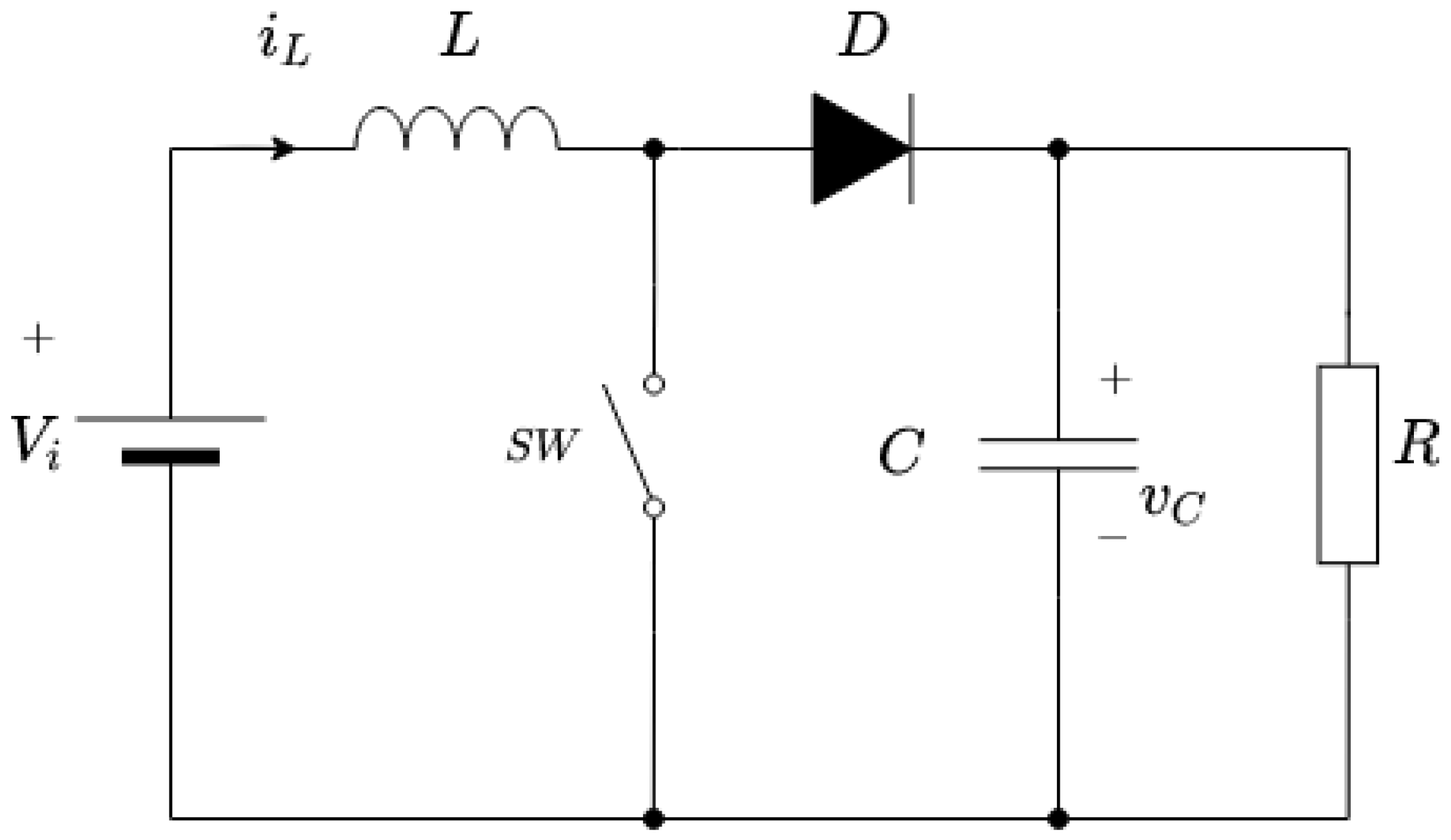
2. State Space Model of Nonlinear CCM Boost Converter

The performance and differences of the non-ideal and ideal system models are investigated in several studies [6,20]: the system non-idealities can be the DC resistance of the inductor, capacitor, and a switching element, and furthermore, the drop voltage on the diode. It is therefore concluded that the non-idealities have minimal influence on the system. Our novel FBL has presented a simplified boost converter model, shown in Figure 1.
The state-space model’s derivation needs to apply the Kirchhoff laws during the switching period. The operation of the boost converter in CCM (continuous conduction mode) can be divided into two phases. Accordingly, when S W is conducted (on-state), the inductor is charged through V i , and the D diode is reverse biased. There is no current flow between the capacitor and the resistor. Thus,
v i = L i L ˙ , 0 = C u C ˙ + u C R .
The state derivative is:
i ˙ L = 1 L v i , u ˙ C = u C R C .
During off-state, the diode will be forward-biased, and the energy of the inductor is toward to load. This means a higher voltage at the output:
a u c = v i L i L ˙ , i L = C u C ˙ + u C R .
The state derivative is:
i ˙ L = u C L + v i L , u ˙ C = i L C u C R C .
The averaged system equation of the CCM boost converter is given by:
c i ˙ L = 1 L ( v i u C + d u C ) , u ˙ C = 1 C ( i L u C R + d i L ) .
In matrix form:
d d t c i L u C = 0 ( 1 d ) L ( 1 d ) C 1 R C i L u C + 1 L 0 v i ,
where i L and u C represent the inductor current and capacitor voltage (output voltage), v i is the input DC voltage, R , L , C symbolize the output load, inductance, and capacitance, and d denotes the duty cycle of the converter.
A SISO (single-input, single-output) nonlinear system can be given by:
l l x ˙ = f ( x ) + g ( x ) u , y = h ( x ) ,
where (from (5))
f ( x ) = 1 L u C + 1 L v i 1 C i L 1 R C u C ,
g ( x ) = 1 L u C 1 C i L .
In another conception, if the control variable is 1 u :
f ( x ) = V i L 1 R C u C ,
g ( x ) = 1 L u C 1 C i L .

3. Principle of State Feedback Linearization

The SISO nonlinear system is given in the form corresponding to (3). It can apply FBL if the following two conditions are satisfied:
  • the rank [ g a d f g a d f n 1 g ] of system matrix should be equal with system dimension;
  • The vector field is involutory in x = x 0 .
The rank of the system matrix of the CCM boost convert is
g ( x ) a d f g ( x ) = u C L u C R L C i L C V i L C + i L R C 2 ,
which equals 2 and the system dimension is 2, so the first condition is satisfied. Accordingly, it needs to exist an output function ( h x ) set the relative degree of the system r = 2.
An approach to obtain the input-output linearization of the boost converter is needed to differentiate the output function by time until the input appears [6,31]:
y ˙ = h x f ( x ) + h x g ( x ) ,
where L f h and L g h mean Lie derivative of h ( x ) along f ( x ) and g ( x ) , respectively. Differentiating y continuously until L g L f h ( x ) 0 , L g L f r 1 h ( x ) 0 , a relative degree of the system is equal with r. The result is: z 1 = y , z 2 = y ˙ , z 3 = y ¨ etc., whose r t h element is:
y ( r ) = L f r h ( x ) + L g L f ( r 1 ) h ( x ) u .
The new control input is given:
v = L f r h ( x ) + L g L f ( r 1 ) h ( x ) u .
The original input of the system is:
u = L f r h ( x ) + v L g L f ( r 1 ) h ( x ) .
The state-space description of the system is [31]:
z 1 ˙ z 2 ˙ z 3 ˙ z r ˙ = 0 1 0 0 0 0 1 0 0 0 0 1 0 0 0 0 A z 1 z 2 z r 1 z r + 0 0 0 1 B v

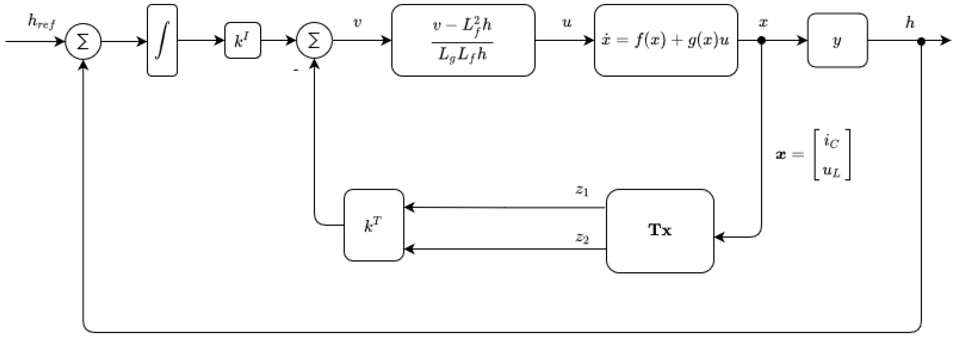
4. Controller Design Applying Exact Feedback Linearization with Integrator

Let the controlled quantity:
y = u C .
We differentiate y with the respective time, and get:
y ˙ = i L C u C R C d i L C .
It is clearly shown, that the relative degree of the system is r < n . In order to g ( x ) = 0 , we choose a new state variable, therefore:
h ( x ) x [ g ( x ) ] = 0 .
A non-trivial solution of Equation (20) is given by Ref. [13]:
h ( x ) = 1 C i L 2 + 1 L u C 2 .
Accordingly, the transformation matrix is given by:
z z ˙ = z 1 z 2 = z = T ( x ) = h ( x ) L f h ( x ) ,
where
L f h = 2 V i i L L C 2 u C 2 R L C .
The new control input is given by applying Equation (8):
u = L f r h ( x ) + v L g L f ( r 1 ) h ( x ) ,
where
L f 2 h = 2 V i 2 C L 2 + 4 u C 2 C 2 L R 2 , L g L f h = 2 V i u C C L 2 4 i L u C C 2 L R .

Reference Value Calculation

The output controllable variable of the system in steady-state is equal with (16): accordingly, the desired control of the original output ( u C ) needs to be properly modified. For this, it is necessary to search for each u C correspondent steady-state value of i L . From Equation (1) d and i L are found (by nullifying the time derivatives), so [26]:
d = u C V i V i , i L = U r e f R 1 u C V i V i .
As a result, the reference is given:
h r e f = ( U r e f R 1 u C V i V i ) 2 C + ( U r e f ) 2 L .
The block scheme of the whole system is shown in Figure 2.

5. Simulation Results

5.1. Examined Scenario

The previously introduced boost converter structure was analyzed during the analysis, and the electrical circuit is shown in Figure 1. To make the results more comparable, we chose an article whose results are validated by real measurements: [32]. Accordingly, the parameters of the examined system are summarized in Table 1. Two parallel connected resistances realize the nominal load to examine the circuit’s dynamical behavior, where one has 70 Ω nominal value, while the second one has 500 Ω . During the simulation, the 70 Ω resistance was turned off after 150 ms and turned on after 400 ms from the starting point. The length of the simulation time is 430 ms.
The reference paper [32] examined the above simulated electrical circuit by a two-loop controller. The control frame of this regulation was reproduced in the Matlab Simulink environment and used for validation. The realized block schema is illustrated in Figure 3. It can be seen in the picture that this controller creates an error signal from the reference voltage ( v r e f ) and the output voltage, which is denoted by u c . The G v denotes the voltage loop gain, which value was selected to 1000, while the G i was selected to 1500.

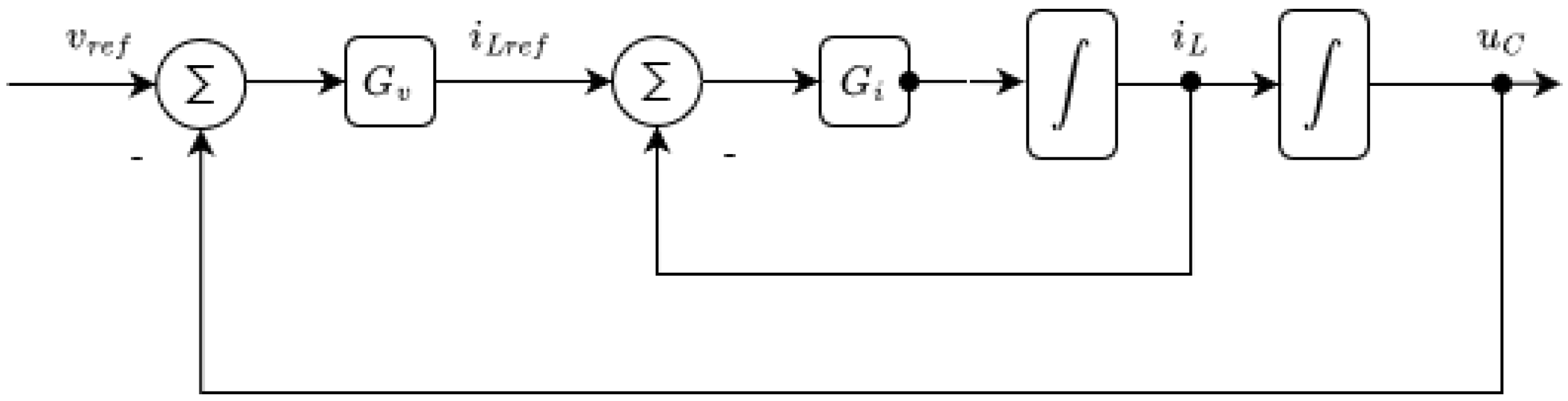
5.2. Linear Controller Design

This section shows the calculation of the required block scheme parameters for the proposed integrator-based control frame Figure 2. Because the examined system is second-ordered, two parameters ( k T and k I ) were used, which form the feedback gain matrix determined in this section. Due to this, the controller was realized by pole placement method [33], and k T and k I can be determined as the closed-loop system poles. Firstly the time constant of the system [13] can be calculated in the following way:
τ = L R = 4   m H 61.4   Ω = 65.1   u s .
Applying the pole-placement methodology [33], at the beginning the poles are placed at the following position:
p = 1 5 τ .
The resulting final values of the poles are:
p = [ 1 / 0.001 ; 1 / 0.001 ; 1 / 0.0004 ] .
From these values, the resulting feedback gain matrix is given:
k T = [ 5.56 · 10 6 , 2.52 · 10 4 ] , k I = [ 3.0864 · 10 8 ] .
It can be seen from the results that the k T and k I values are relatively high because we have not used a coherent system of units, and the SI units give all parts of the system.

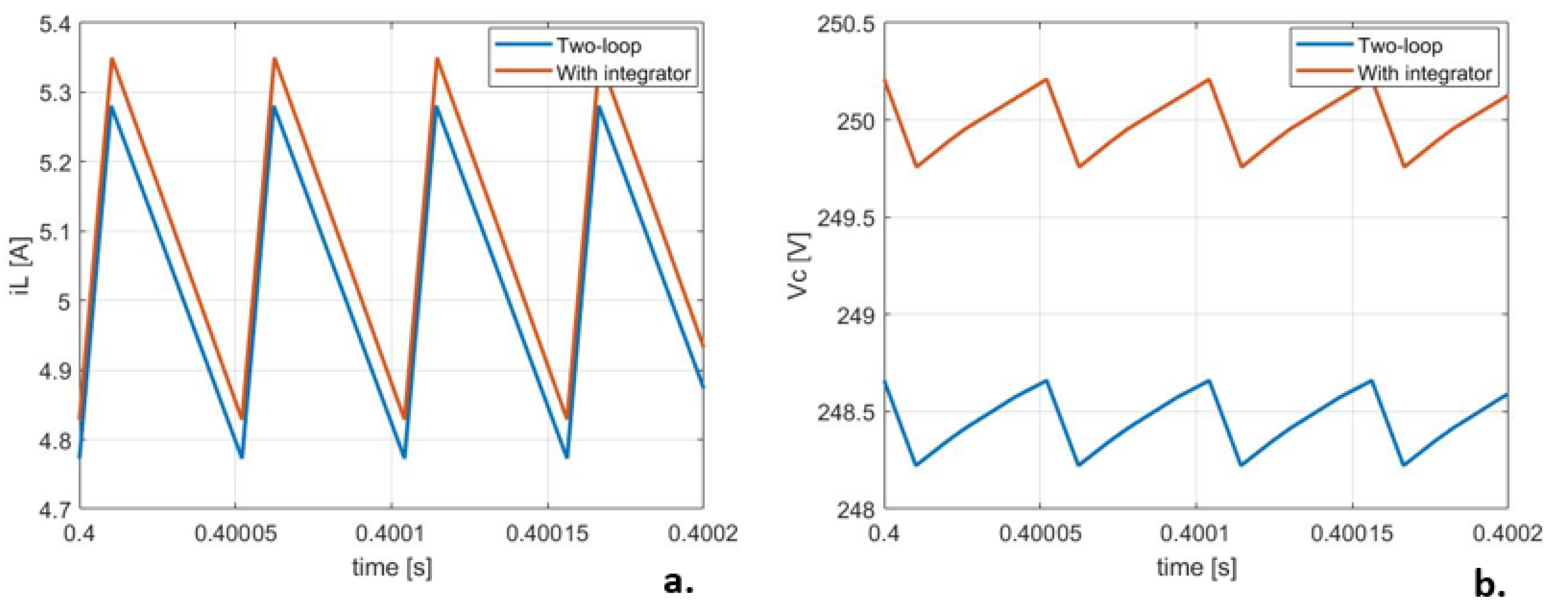
5.3. Steady-State Behavior

Figure 4 shows the steady-state results of inductor current ( i L ) and output (capacitor) voltage ( u c ) in the case of the reference (two-loop controller) and the proposed control methodology. The steady-state begins from 400 ms, when the transient finished. The reference methodology is denoted by a two-loop controller label, while the proposed methodology is referred to with integrator label in the following part of the paper. Figure 4, a compares the resulting signal of the inductor current ( i L ), where the resulting value of the proposed controller coincides with the reference. It can be seen from Figure 4b that the proposed methodology is more accurate than the reference, because the resulting time-function of the output voltage is more close to the expected value of V c .

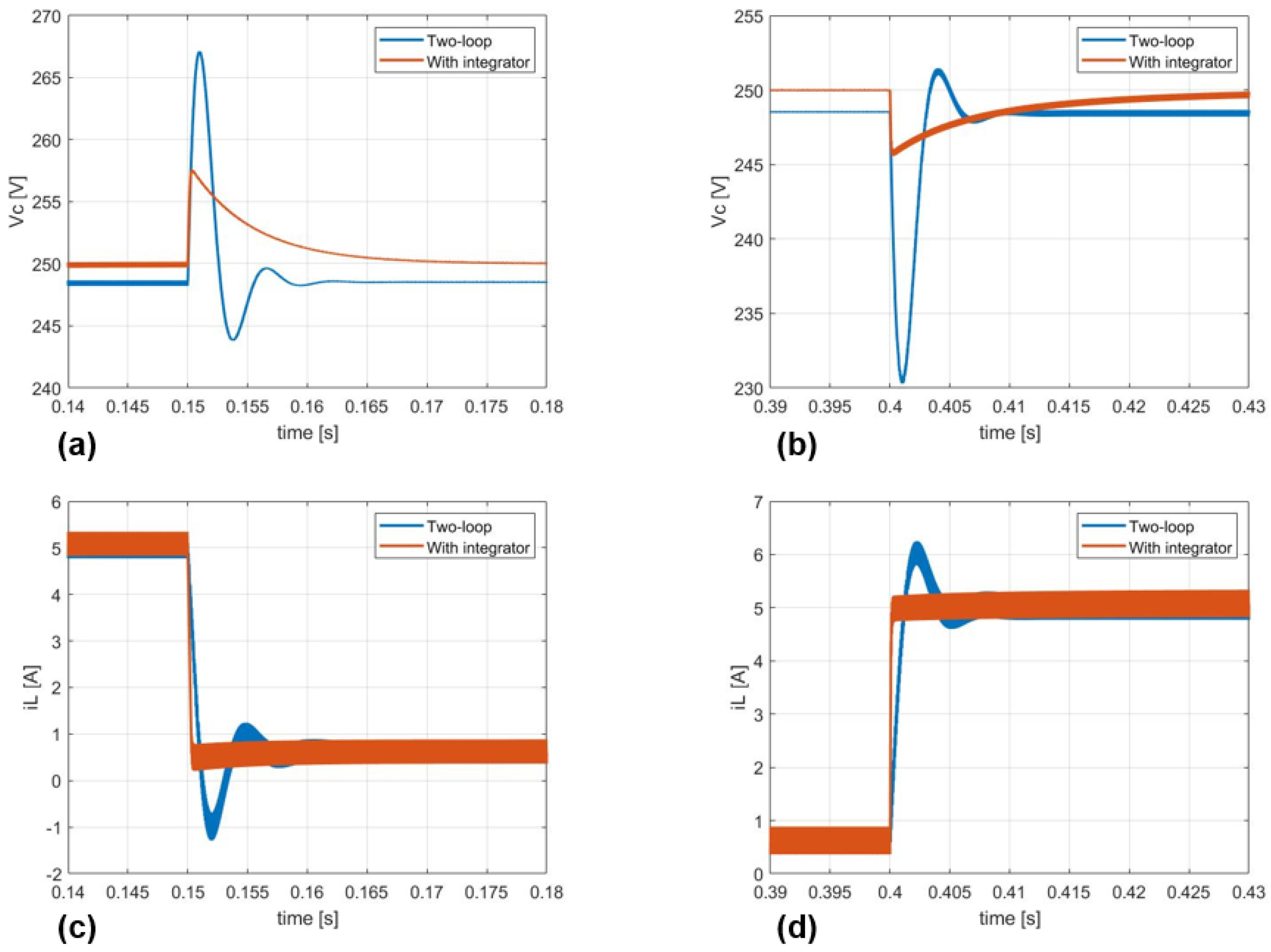
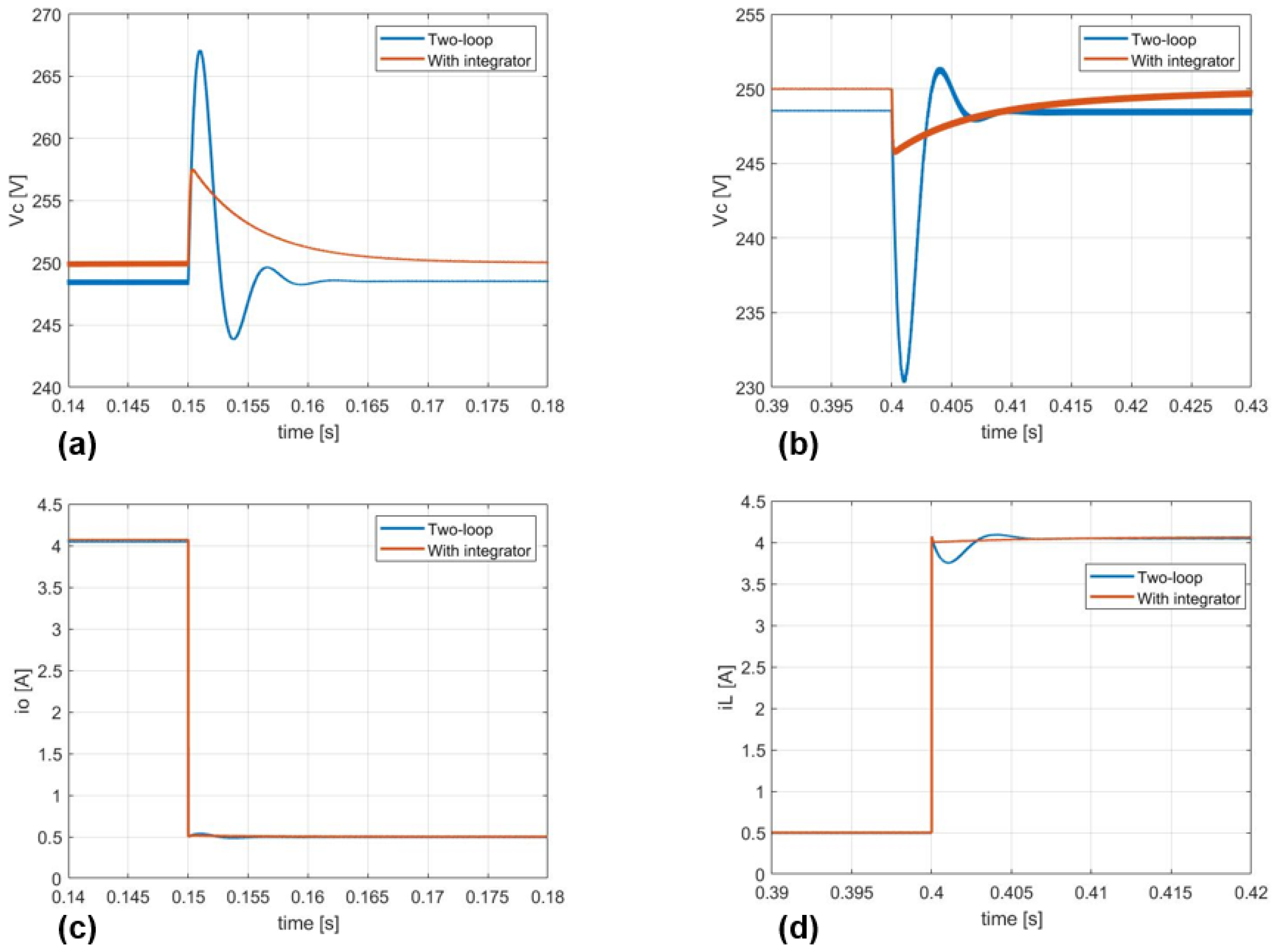
5.4. Dynamic Behavior

Figure 5 shows the system’s dynamical behavior. The load change realized this dynamic response: the 70 Ω resistance turned off after 150 ms and then switched on after 400 ms from the start signal. Figure 5a,c shows the output voltage and the inductor current of the converter during the switch off of the 70 Ω resistance, while the Figure 5b,d images show the changes of the same quantities around the switch-on moment of the 70 Ω resistance (400 ms). It can be seen from Figure 5a that the amplitude of the transient in the proposed system is smaller than the reference, the two-loop controlled system. The time of the transient process takes nearly the same time during the two compared solutions. The reference system converges to 248 V after the transient, which means a relatively small, around a 2 V (0.8%) steady-state error, while the proposed, integrator-based system converges to the expected value (250 V). If we see Figure 5c, which shows the inductor current—the non-controlled quantity—during the same process, it can be seen that the integrator-based solution does not have huge amplitude imbalances during the control process.
It can be seen from Figure 5b that the transient error (deviation from nominal output voltage) in the case of the reference controller is about 20 V, while for the previous switch-on process it was 17 V, as shown in Figure 5a. The proposed integrator-based controller has a significantly smaller transient amplitude, smaller than the half of the two-loop controlled systems response; it is about 7 V in both of the examined cases.
Figure 6a,b show the controlled voltages during the switch-off and switch-on process of the controlled 70 Ω resistance. These images are the same as in Figure 5a,b, while Figure 6c,d shows the output currents of the realized controllers. A slight difference can be seen in Figure 6d, which shows a small transient in the output current. However, there is no significant difference between the controlled output currents of the proposed and the reference two-loop controlling schemes.
The duty-cycle of the proposed controller is shown in Figure 7. The first image (Figure 7a) shows the calculated duty cycle during the switch-off, while Figure 7b shows the process of the loading resistance. We can here see the fast response of the proposed controller.
Finally, it can be seen from the results that the steady-state behavior of the two-loop based feedback linearization—what we used as a validated reference—has about 1% error [32] on that system, where the proposed integrator-based controller can reduce the error significantly, nearly to zero. It can be seen in Figure 5 and Figure 6, that the dynamic behavior has also improved. The overshoot in the output voltage is decreased from 6% to 2%. Based on these simulation results, it can be concluded that the presented control method has significantly better steady-state and dynamic behavior than the compared two-loop control schema.

6. Conclusions

In this article, the novel form of direct feedback linearization controlled boost converter has been presented. Most of the papers apply classic control theory. Therefore these approaches linearize a non-linear system, which generally leads to steady-state error. This problem can be eliminated by applying non-linear methods. This paper proposed an error integrator in the control loop. As a result of this modification, the control of the output voltage response is improved significantly. As can be seen from the comparison of the two-loop controller on the same converter, both the steady-state and the dynamical behavior improved significantly in the examined system. Moreover, the paper proposed the usage of the pole-placement method to make a faster and more robust design of the internal linear controller. The proposed methodology can be used to develop a generalized framework. Further research should be carried out to establish a methodology for robust behavior with more accurate load and parameter estimation. Moreover, the physical realization of the proposed methodology is planned in the laboratory.

Author Contributions

Conceptualization, M.C. and M.K.; methodology, M.C. and M.K.; software, M.C. and M.K.; validation, M.C.; formal analysis, M.C., T.O. and M.K.; investigation, M.C.; resources, M.C. and M.K.; data curation, M.C.; writing—original draft preparation, M.C.; writing—review and editing, M.C., T.O. and M.K.; visualization, M.C.; supervision, M.K.; project administration, M.C.; funding acquisition, T.O. All authors have read and agreed to the published version of the manuscript.

Funding

This research received no external funding.

Institutional Review Board Statement

Not applicable.

Informed Consent Statement

Not applicable.

Data Availability Statement

Not applicable.

Conflicts of Interest

The authors declare no conflict of interest.

References

  1. Shepherd, W.; Zhang, L. Power Converter Circuits; Marcel Dekker, Inc.: New York, NY, USA, 2004. [Google Scholar]
  2. Alatai, S.; Salem, M.; Ishak, D.; Das, H.S.; Alhuyi Nazari, M.; Bughneda, A.; Kamarol, M. A Review on State-of-the-Art Power Converters: Bidirectional, Resonant, Multilevel Converters and Their Derivatives. Appl. Sci. 2021, 11, 10172. [Google Scholar] [CrossRef]
  3. Mumtaz, F.; Yahaya, N.Z.; Meraj, S.T.; Singh, B.; Kannan, R.; Ibrahim, O. Review on non-isolated DC-DC converters and their control techniques for renewable energy applications. Ain Shams Eng. J. 2021, 12, 3747–3763. [Google Scholar] [CrossRef]
  4. Hemasuk, K.; Po-Ngam, S. The simplified regenerative boost converter for electric vehicle applications. In Proceedings of the 2017 International Electrical Engineering Congress (iEECON), Pattaya, Thailand, 8–10 March 2017; pp. 1–4. [Google Scholar]
  5. Prabhakar, S.; JL, F.D. A comparative study on the performance of interleaved converters for EV battery charging. In Proceedings of the 2016 IEEE 6th International Conference on Power Systems (ICPS), New Delhi, India, 4–6 March 2016; pp. 1–6. [Google Scholar]
  6. Mohanty, P.R.; Panda, A.K.; Das, D. An active PFC boost converter topology for power factor correction. In Proceedings of the 2015 Annual IEEE India Conference (INDICON), Online, 17–20 December 2015; pp. 1–5. [Google Scholar]
  7. Leoncini, M.; Levantino, S.; Ghioni, M. Design issues and performance analysis of CCM boost converters with RHP zero mitigation via inductor current sensing. J. Power Electron. 2021, 21, 285–295. [Google Scholar] [CrossRef]
  8. Almawlawe, M.D.H.; Kovandzic, M. A Modified Method for Tuning PID Controller for Buck-Boost Converter. Int. J. Adv. Eng. Res. Sci. 2016, 3, 20–26. [Google Scholar] [CrossRef]
  9. Bouziane, H.A.; Bouiadjra, R.B.; Debbat, M. Design of robust LQR control for DC-DC multilevel boost converter. In Proceedings of the 2015 4th International Conference on Electrical Engineering (ICEE), Boumerdes, Algeria, 13–15 December 2015; pp. 1–5. [Google Scholar]
  10. Prasad, G.; Kumar, A. A Comparison Between Sliding Mode Control and Feedback Linearization. In Proceedings of the 2018 5th IEEE Uttar Pradesh Section International Conference on Electrical, Electronics and Computer Engineering (UPCON), Gorakhpur, India, 2 November 2018; pp. 1–5. [Google Scholar] [CrossRef]
  11. Mandal, S.; Mishra, D. Robust Control of Buck Converter using H-infinity Control Algorithm. In Proceedings of the 2018 IEEE Applied Signal Processing Conference (ASPCON), Kolkata, India, 7–9 December 2018; pp. 163–167. [Google Scholar] [CrossRef]
  12. Zheng, H.; Shuai, D. Nonlinear control of Boost converter by state feedback exact linearization. In Proceedings of the 2012 24th Chinese control and decision conference (CCDC), Taiyuan, China, 23–25 May 2012; pp. 3502–3506. [Google Scholar] [CrossRef]
  13. Csizmadia, M.; Kuczmann, M. Extended Feedback Linearisation Control of Non-ideal DCDC Buck Converter in Continuous-conduction Mode. Power Electron. Drives 2022, 7, 1–8. [Google Scholar] [CrossRef]
  14. Saraf, P.; Gupta, M.; Parimi, A.M. A Comparative Study Between a Classical and Optimal Controller for a Quadrotor. In Proceedings of the 2020 IEEE 17th India Council International Conference (INDICON), New Delhi, India, 10–13 December 2020; pp. 1–6. [Google Scholar] [CrossRef]
  15. Huang, H.; Zhang, C.; Ding, W.; Xinke, Z.; Sun, G.; Wang, H. Design of the Depth Controller for a Floating Ocean Seismograph. J. Mar. Sci. Eng. 2020, 8, 166. [Google Scholar] [CrossRef]
  16. Utkin, V.; Lee, J. Chattering Problem in Sliding Mode Control Systems. In Proceedings of the International Workshop on Variable Structure Systems, Alghero, Italy, 5–7 June 2006; pp. 346–350. [Google Scholar] [CrossRef]
  17. Komurcugil, H.; Biricik, S.; Bayhan, S.; Zhang, Z. Sliding Mode Control: Overview of Its Applications in Power Converters. IEEE Ind. Electron. Mag. 2021, 15, 40–49. [Google Scholar] [CrossRef]
  18. Bevrani, H.; Abrishamchian, M.; Safari-Shad, N. Nonlinear and linear robust control of switching power converters. In Proceedings of the 1999 IEEE International Conference on Control Applications (Cat. No.99CH36328), Kohala Coast, HI, USA, 22–27 August 1999; Volume 1, pp. 808–813. [Google Scholar] [CrossRef] [Green Version]
  19. Implementing a PID Controller Using a PIC18 MCU, AN937, Microchip Technology Application Note. AN937, Application Note 2004. Available online: http://www.t-es-t.hu/download/microchip/an937a.pdf (accessed on 13 October 2022).
  20. Ming, W.; Liu, J. A new experimental study of input-output feedback linearization based control of Boost type DC/DC converter. In Proceedings of the 2010 IEEE International Conference on Industrial Technology, Vina del Mar, Chile, 14–17 March 2010; pp. 685–689. [Google Scholar]
  21. Accetta, A.; Cirrincione, M.; D’Ippolito, F.; Pucci, M.; Sferlazza, A. Input-Output Feedback Linearization Control with On-Line Inductances Estimation of Synchronous Reluctance Motors. In Proceedings of the 2021 IEEE Energy Conversion Congress and Exposition (ECCE), Vancouver, BC, Canada, 10–14 October 2021; pp. 4973–4978. [Google Scholar] [CrossRef]
  22. Khazaei, J.; Tu, Z.; Asrari, A.; Liu, W. Feedback Linearization Control of Converters with LCL Filter for Weak AC Grid Integration. IEEE Trans. Power Syst. 2021, 36, 3740–3750. [Google Scholar] [CrossRef]
  23. Dini, P.; Saponara, S. Cogging torque reduction in brushless motors by a nonlinear control technique. Energies 2019, 12, 2224. [Google Scholar] [CrossRef] [Green Version]
  24. Dini, P.; Saponara, S. Electro-Thermal Model-Based Design of Bidirectional On-Board Chargers in Hybrid and Full Electric Vehicles. Electronics 2021, 11, 112. [Google Scholar] [CrossRef]
  25. Dini, P.; Saponara, S. Model-Based Design of an Improved Electric Drive Controller for High-Precision Applications Based on Feedback Linearization Technique. Electronics 2021, 10, 2954. [Google Scholar] [CrossRef]
  26. Cervone, A.; Brando, G. Input-State Feedback Linearization of a Boost DC/DC Converter; ELECTRIMACS 2019 Selected Papers; Walter, Z., Giovanni, P., Eds.; Springer: Berlin/Heidelberg, Germany, 2020; Volume 1, pp. 139–153. [Google Scholar] [CrossRef]
  27. Lucas, K.E.; Pagano, D.J.; Plaza, D.A.; Vaca-Benavides, D.A.; Ríos, S.J. Robust feedback linearization control for DAB converter feeding a CPL. IFAC-PapersOnLine 2020, 53, 13402–13409. [Google Scholar] [CrossRef]
  28. Wu, J.; Lu, Y. Feedback linearization adaptive control for a buck converter with constant power loads. In Proceedings of the 2018 IEEE International Power Electronics and Application Conference and Exposition (PEAC), Shenzhen, China, 4–7 November 2018; pp. 1–6. [Google Scholar]
  29. Bhattacharyya, D.; Padhee, S.; Pati, K.C. Modeling of DC–DC converter using exact feedback linearization method: A discussion. IETE J. Res. 2019, 65, 843–854. [Google Scholar] [CrossRef]
  30. Salimi, M.; Siami, S. Cascade nonlinear control of DC-DC buck/boost converter using exact feedback linearization. In Proceedings of the 2015 4th International Conference on Electric Power and Energy Conversion Systems (EPECS), Sharjah, United Arab Emirates, 24–26 November 2015; pp. 1–5. [Google Scholar]
  31. Liu, J.; Ming, W.; Gao, F. A new control strategy for improving performance of boost DC/DC converter based on input-output feedback linearization. In Proceedings of the 2010 8th World Congress on Intelligent Control and Automation, Jinan, China, 7–9 July 2010; pp. 2439–2444. [Google Scholar] [CrossRef]
  32. Liu, X.; Lin, X.; Xu, F.; Kang, Y. Research on Boost converter based on nonlinear control strategy. In Proceedings of the 2009 IEEE 6th International Power Electronics and Motion Control Conference, Wuhan, China, 17–20 May 2009; pp. 1329–1334. [Google Scholar] [CrossRef]
  33. Keviczky, L.; Bars, R.; Hetthéssy, J.; Bányász, C. Control Engineering; Advanced Textbooks in Control and Signal Processing; Springer: Singapore, 2018. [Google Scholar]
Figure 1. Circuit diagram of the boost converter.
Electronics 12 00057 g001
Figure 2. The schematic view of the feedback linearization with an error integrator-based control frame.
Electronics 12 00057 g002
Figure 3. The image shows the simplified block scheme of the two-loop nonlinear control, which was applied in the reference paper.
Electronics 12 00057 g003
Figure 4. Simulation result in the steady-state of the (a) inductor current and (b) output voltage in the case of the different control schemes.
Electronics 12 00057 g004
Figure 5. (a,c) The transient response of the proposed and the reference system during the switching-off procedure. (b,d) The same output voltage ( V c ) and current quantities ( i L ) during the switch-on process of the 70 Ω resistance.
Electronics 12 00057 g005
Figure 6. (a,b) The controlled voltage during the switching-off and the switching on procedures. (c,d) The output currents ( i o ).
Electronics 12 00057 g006
Figure 7. Dutycycle during load variation in the case of the proposed controller. (a) The switch-off phase of the 70 Ω load, and (b) the duty cycle during the switch-on phase.
Electronics 12 00057 g007
Table 1. Specified parameters of the examined boost converter.
ParameterSymbolSpecification
Nominal loadR61.4 Ω
Boost inductorL4 mH
Boost filter capacitorC94 μ F
Input voltage V i n 200 V
Output voltage V o 250 V
Output current I o 4 A
Switching frequency f s w 19.2 kHz
Disclaimer/Publisher’s Note: The statements, opinions and data contained in all publications are solely those of the individual author(s) and contributor(s) and not of MDPI and/or the editor(s). MDPI and/or the editor(s) disclaim responsibility for any injury to people or property resulting from any ideas, methods, instructions or products referred to in the content.

