Abstract
In this study, trench sidewall modification processes were designed to improve profile uniformity and thereby enhance the electrical performance of silicon power devices in large-scale production. The effects of trench sidewall modification on the morphology, structure and electrical properties were studied. Plasma-induced damage in etching processes was also observed and briefly explained. Straight and smooth sidewall profiles were achieved through adjusting the SF6/CHF3 proportion in a combined etchant gas flow in the main etching procedure. By comparing HRSEM images from different etching protocols, it was evident that an enhanced CHF3 flow formed a proper passivation of the sidewall, eliminating the ion damages that are common in current main etch steps. To address the impurities introduced from the etchant gas and improve the gate oxide uniformity, further steps of depolymerization were applied in a plasma asher chamber, followed by wet clean steps. In the meantime, the plasma-induced charge accumulation effect was reduced by UV curing. Improved trench sidewall profiles and the gate oxide uniformity contributed to a lower leakage current between the gate and source terminals, leading to an overall yield enhancement of device properties in large-scale silicon wafer fabrication.
1. Introduction
As with rapid developments in consumer electronics and electric vehicles, silicon power devices play an increasingly crucial role [1]. Compared with silicon planar devices, which were the main application devices, trench structures enable a much smaller drain on resistance (Rdson) for the same chip area, significantly reducing overall conduction losses [2,3]. As the key stage in silicon power MOSFET manufacturing, trench etching processes directly influence the effect of subsequent processes as well as device performance. Ideal etching processes exhibit the following characteristics [2,4]:
- Anisotropic etching that requires a surface reaction to proceed in only the vertical direction without lateral undercutting. In this way, we are able to ensure that the exact same geometry as on the resist is accurately replicated on the etched film;
- Good etching selectivity that permits the etching rate of the resist, used as a mask, and the layer below, such as SiO2 or Si3N4, to be much smaller than the etching rate of the etched film; this ensures the effectiveness of resist masking during the process by avoiding potential damages to other materials beneath the film from over-etching;
- Large batch processing with reliability and reproducibility, low cost and minimal environmental pollution, as are the requirements for production on an industrial scale.
Moreover, silicon etching of devices has high requirements for the accuracy of etching topography under high control precision. The Bosch process has been applied in the fabrication of deep-trench devices such as MEMS devices and silicon photodetectors [4,5,6]. The advantages of the Bosch process are its high etching verticality and excellent rate uniformity, as well as a high ratio and good repeatability. However, the Bosch process will inevitably form scalloped wrinkles on the sidewalls, which will affect the polysilicon backfill process and lead to device breakdown. Researchers have attempted a variety of methods to eliminate sidewall scallop wrinkles, but these methods are difficult to apply to the trench etching process of power devices due to possible contamination by metal ions or complicated processes and insignificant effects [7]. Inductively coupled plasma (ICP) etching is another common etching method that is compatible for Spilt-Gate trench (SGT) devices in terms of its large depth/width aspect ratios [8]; however, the sidewall topography requirements for the 5:1 aspect ratio required for trench power devices are hardly met.
Reactive-ion etching (RIE) with a directional etching process that utilizes ion bombardment to remove material has been adopted for low-voltage silicon device fabrication, and previous investigations regarding etching processes have concentrated on its relationship to process parameters, such as gas flow rate, temperature and pressure [9]. Reactive free radicals generated from F-, Cl- and Br-based etching gases react with silicon to easily form vaporized species [10]. Layers of polymer films condensed by etching gases and side products on the surface of the side wall reduce the lateral etching to a certain extent. A dynamic equilibrium established between vertical processes and lateral polymerization gives rise to a smooth sidewall profile control [11]. However, large-scale wafer production could involve much more reactant gases, such as HBr, CHF3 and O2, and the temperature and radio frequency (RF) power should also be taken into consideration [4]. In this case, we studied the effects of various etching atmospheres on the trench silicon structure to obtain a smooth sidewall profile and uniform interface between gate oxide and silicon, aiming to determine the relationship between trench etching process parameters and morphology and the silicon power device electric parameter. Furthermore, we found that a SF6-rich etching atmosphere and plasma-induced charge accumulation effect caused a jagged sidewall morphology that plays a critical role in the current leakage between the gate and source terminals. By using an optimized dry etching and wet polymer removal process, uneven sidewalls and gate oxide current leakage can be effectively solved, and such pathways also illustrate a reliable solution for fabricating high-yield, low-voltage, trench structure power devices.
2. Methodology
The silicon trench fabrication process is illustrated in Figure 1. Prior to the silicon etching process, hard mask (HM) deposition and a lithography process (critical dimension: 0.3 μm) were conducted using a phosphorus-doped silicon epitaxy wafer (725 μm, 8 inches) as the substrate. To evaluate the sidewall uniformity of the silicon trench, the etching process was divided into main etching and over etching steps to form the silicon trench and bottom rounding effect.

Figure 1.
Fabrication process of the silicon trench structure.
To further investigate the electric properties, a simulation of the fabrication of a low-voltage trench silicon device is illustrated in Figure S1. For sample fabrication, HM removal and sacrifice oxide removal were conducted after the trench etching procedures, the trench structure was filled with 600 A gate oxide and 8000 A doped poly-silicon. After the oxide interlayer dielectric SiO2 was formed (PECVD, 7000 A), contact hole opening (CD: 0.35 μm) and metal deposition were performed. The silicon wafers were ground to 200 μm to lower the drain-source on-state resistance; the backside electrode Ti/Ni/Ag was thermally evaporated with thickness of 1.2 K/2.5 K/10 K angstrom, respectively. HRSEM was used to observe the cross-section morphology of the silicon device samples after focus ion beam (FIB) preparation. The I-V test system was used to examine electrical parameters, such as Vth (threshold Voltage), IGSS (gate-source leakage current) and IDSS (drain-source leakage current); the detailed information is listed in Figure S2.
3. Results and Discussion
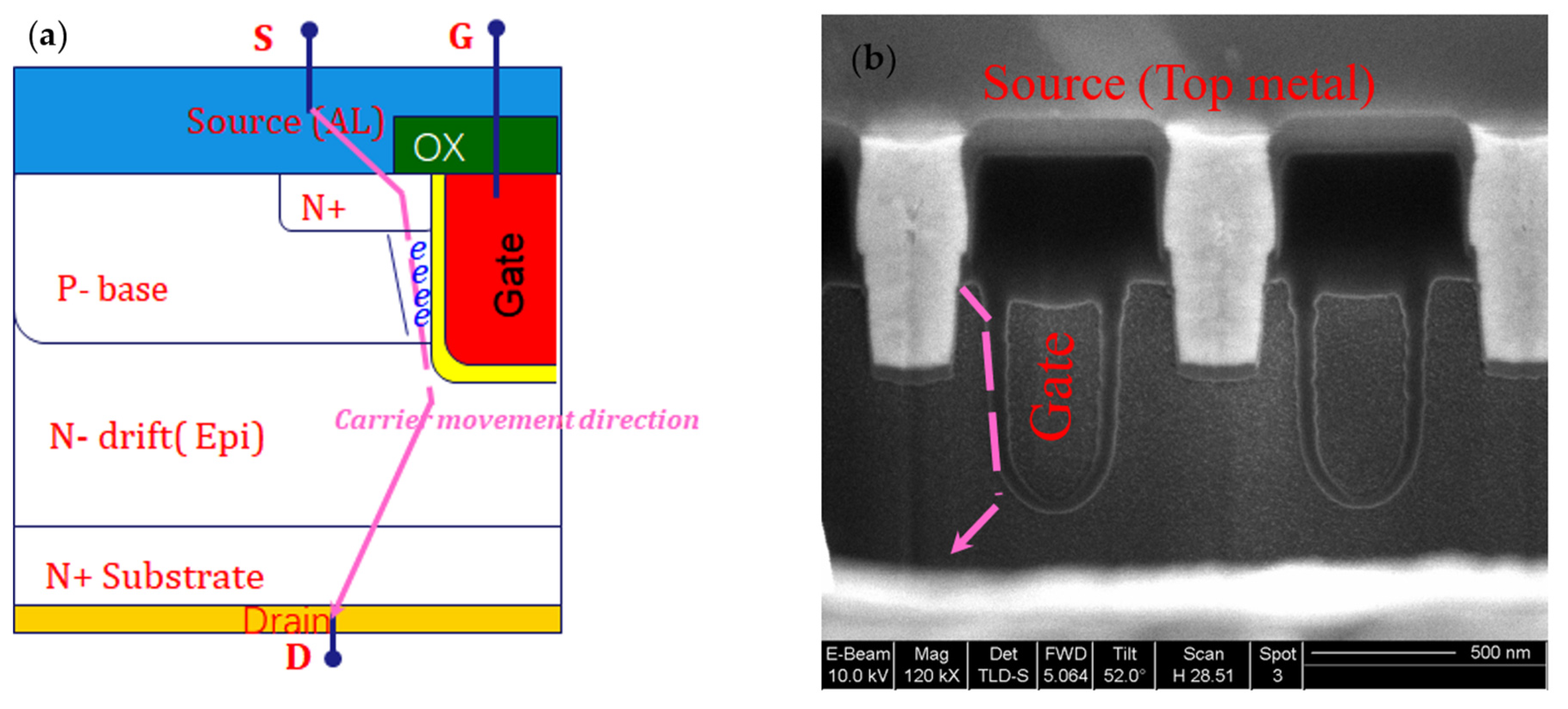
Figure 2a shows a schematic of the trench MOSFET device structure. The source, drain and gate are marked with blue, orange and pink color, respectively; the electron movement direction is also marked with pink color. When positive voltage is applied between the gate and source, a vertical channel is formed in the area adjacent to the P- base and gate. The electron will move from the gate oxide to the drift area and will finally flow vertically through the interior of the wafer to drain into the electrode. It can be seen that the width of the gate is much smaller than that of a vertically conducting planar structure and, therefore, has a smaller cell size and a lower on-state resistance. Figure 2b illustrates the SEM image of the source and gate area; for the source area, the top metal (AlCu) is connected with the N+ region through contact via the hole, gate oxide and gate (doped poly-silicon), which are isolated by interlayer dielectric (ILD).
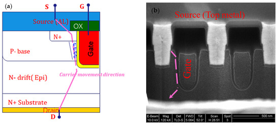
Figure 2.
(a) Schematic diagram of the trench MOSFET device; (b) SEM image of the cross-section regime for gate and source terminals.
There are multiple factors that should be considered in silicon etching processes to form trench structures [10,12]. Etching radicals could react with Si and SiO2 due to the absence of photoresist blocking at this stage, as illustrated by the formulas below:
SF6 + Si → SiF (gas) + S
CHF3+ Si → SiF (gas) + S
CF4 + Si → SiF (gas) + C
C4F8 + SiO2 → SiF (gas) + CO2 (gas)
Unlike the isotropic process of wet etching, silicon dry etching on low-voltage devices focuses on the <100> plane only. Fluorine- and chlorine-based etching gases react with silicon substrates with high etching selectivity. The impact of HM SiO2 on etching parameters, the ultimate profile and electrical performances are not considered here in spite of the losses of SiO2 in this stage due to HM removal after the completion of the etching processes.
3.1. Initial Etching Process
Initial attempts regarding trench etching processes include the breakthrough (BT) step that removes the surface oxides and organic impurities, followed by the main etch (ME)1 and ME2 steps, which are used to form ideal profiles by utilizing the high-efficiency vertical direction. The specific parameters are listed in Table 1.

Table 1.
Etching process parameters for the initial protocol.
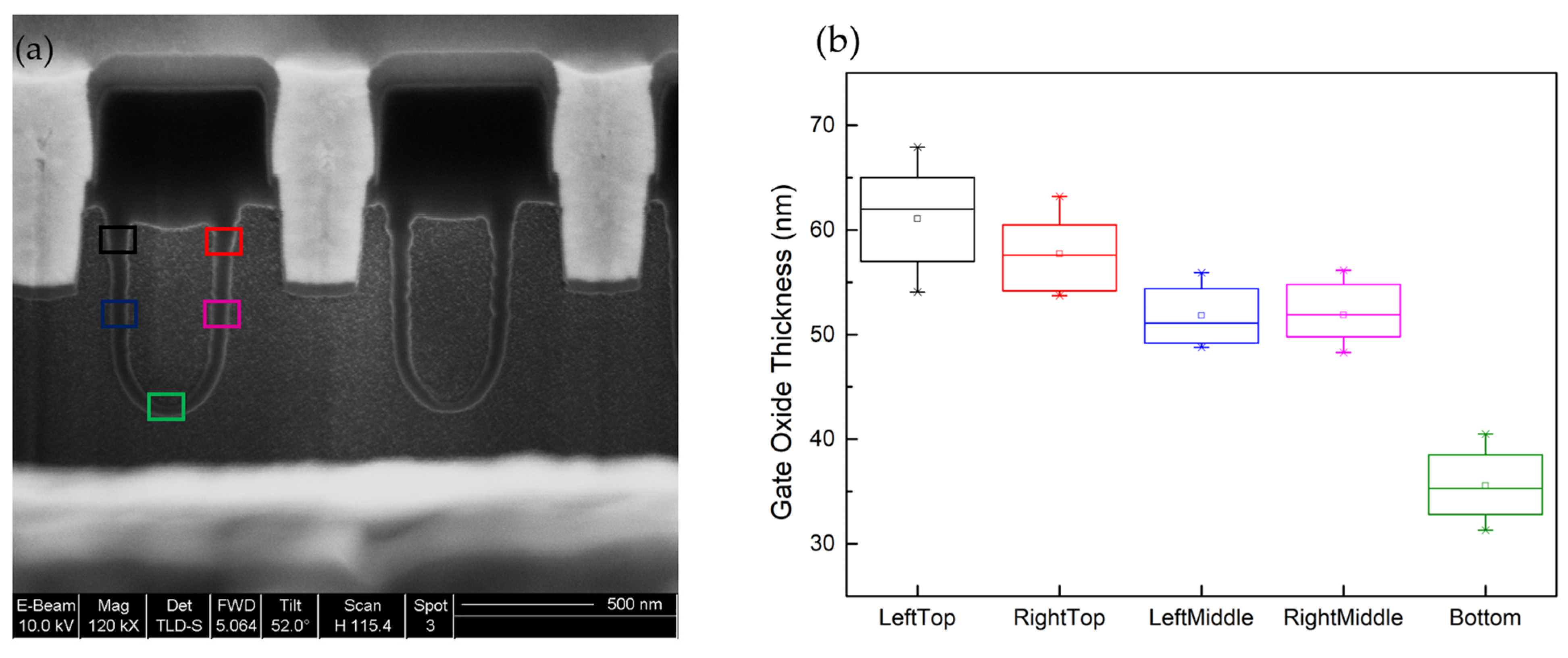
After the completion of the silicon trench etching stage, the uppermost SiO2 HM layer is removed in order to generate gate oxide. Figure 3a shows an HRSEM image of the cross section of a low-voltage silicon trench MOSFET device. An extensive jagged morphology was observed between the gate oxide and silicon interface, demonstrating an uneven distribution of gate oxide thickness. The gate oxide thicknesses of different regions in the trench structure are shown in Figure 3b; the upper region of the trench presented a gate oxide thickness of about 60 nm, but the bottom region only had a thickness of 35 nm. The average thickness of the upper trench region was nearly twice that of the bottom of the trench; the range of thicknesses between each individual region was significant with a gate oxide homogeneity of over 10%. In addition to the HM and sacrifice oxide wet removal processes, which might consume silicon on the top corners of the trench, varied gate-oxide thicknesses could be contributed to gate–oxide formation steps; however, a jagged morphology with uneven thickness could easily be a gate-oxide curvature near the bottom part that could easily cause a breakdown or current leakage [13]. Specifically, plasma-accelerated ions collided with the trench sidewall at a small angle and were reflected to the bottom corners of the sidewall. To examine the microscopic damage, Figure S3 shows the cross-section SEM images using the protocol from Table 1; the interface between the polysilicon and gate oxide showed a jagged morphology that matches the result from Figure 1. The microscope damage may be related to the thickness deviation of hundreds of angstrom in the gate oxide producing an electron shading effect [14,15]. The sheath potential accelerates the ions straight down to reach the bottom of the trench, preparing the area for efficient etching by neutral chlorine atoms. However, the electron charges at the top of the trench, if asymmetric, can distort the ion trajectories so that the ions hit the bottom sidewalls, imparting a positive charge on them. This will result in the formation of a self-consistent distribution of potentials and ion orbits. The charging of the sidewalls will not be symmetrical if the features are not all the same size.

Figure 3.
(a) HRSEM image of the cross section using the initial protocol; (b) gate oxide thickness distribution in different parts of the trench.
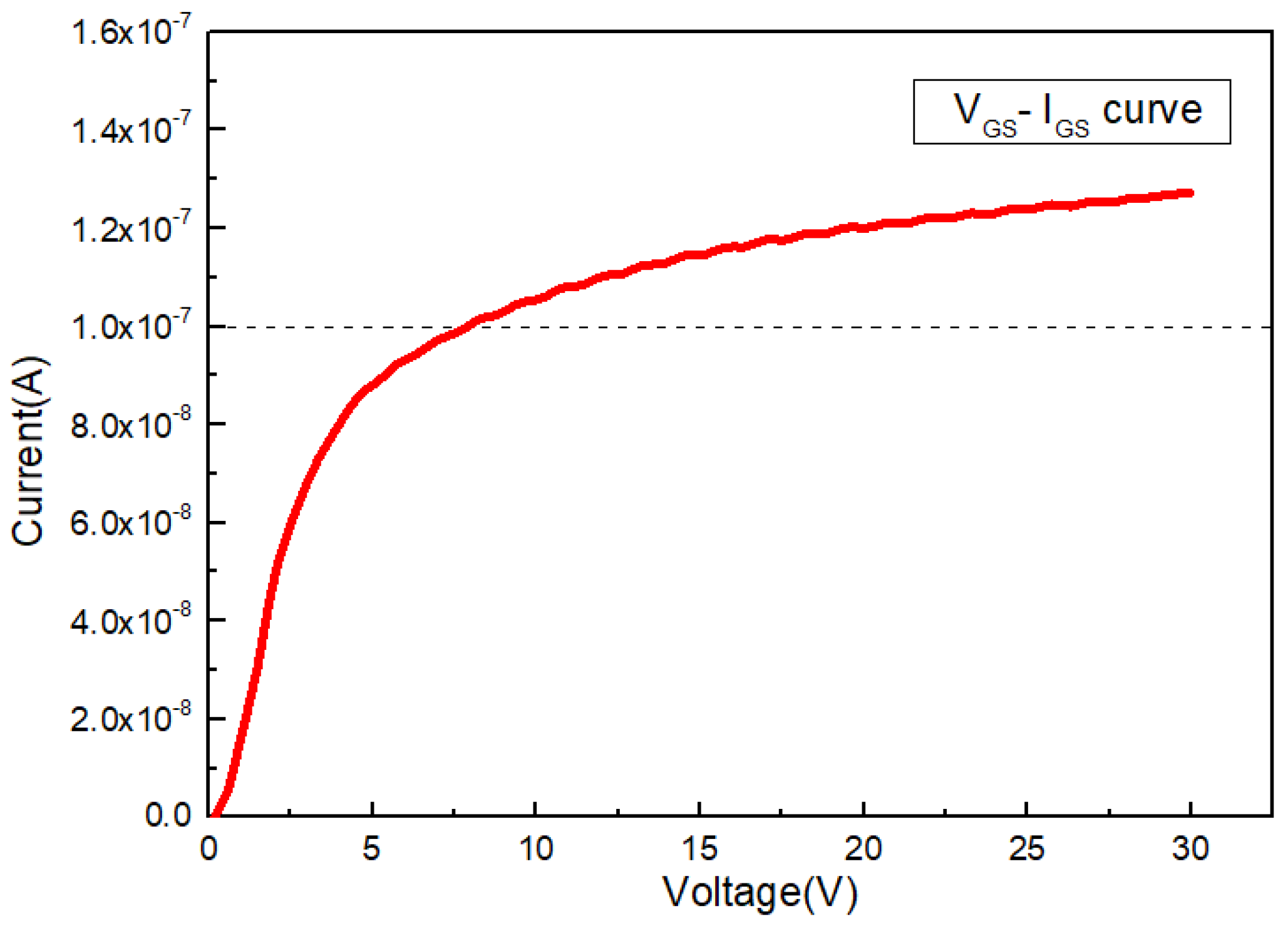
Figure S2 illustrates the bin-map distribution of the yield results for the device and shows that more than 35% of the total cells failed to reach the threshold, especially for the IGSS parameter. The majority of failed dies were distributed in the marginal region of the wafer, which may be related to the etching process [16]. IGSS and Vth tests could elucidate the gate oxide properties by further investigating the relationship between etching protocols and device electrical performances. Figure 4 illustrates the IGSS curve, showing a rising trend with increasing voltage. When the voltage approached 10 V, the current exceeded the threshold of 100 nA [17].
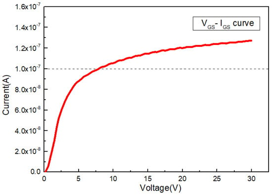
Figure 4.
Gate-source leakage current (Vgs = 20 V) using the initial protocol (60 V trench Mosfet sample), the black dotted line represents for threshold of current.
Figure 5 shows the threshold voltage measurements under the test condition Vgs = 0 V; the current significantly surged as voltage exceeded 0.5 V, demonstrating a low Vth that failed to meet the device requirements. Poor-quality gate oxide may be caused by plasma charging during the etching process. The physical effect of dry etching refers to the bias between the silicon wafer and the plasma, which will accelerate the particles to effectively bombard the silicon wafer surface. Plasma may destroy the surface structure of the wafer since the silicon surface is negatively charged during the etching reaction. Unlike planar MOSFET structures that consider the RF displacement current directly damaging the surface of the gate oxide, ion and electron currents can be collected by a polysilicon gate electrode which works as antenna and the gate oxide layer can be seen as a capacitor. When more and more charge is collected on the gate, the gate voltage increases, eventually causing FN tunneling through the gate oxide. Electron flux balances the loss of positive ions in the plasma region during each RF cycle. At an ideal homogeneous plasma condition, the ion and electron currents are locally balanced over individual RF cycles leading to the surface potential being close to the substrate potential. For a non-uniform plasma distribution scenario, the electron and ion currents are not in a local overall net equilibrium near the electrodes; the presence of net plasma currents leads to local charging on the surface. Polished silicon wafer substrates show a continuous trend with uniform potential; however, the trench and gate terminals are separated and discontinuous. The gate electrodes at different locations have different potentials, and plasma could induce charge accumulation on the trench sidewall and bottom regimes. Charges accumulating on the sidewalls and surface of the trench under the etching atmosphere could lead to damage at the layer interface. The fundamental cause of sidewall interface damage is the uneven distribution of positive ions and electrons when the plasma is generated. The process of releasing a charge is more difficult using high level electronegativity gases, such as SF6 and CF4, which aggravate the non-equilibrium charges in the non-conductor [5,18]. The F-N current effect will occur when the charge accumulates to a certain extent on the surface, which leads to gate oxide layer damage.
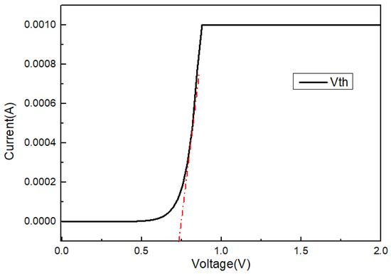
Figure 5.
Threshold voltage measurement (VDS-IDS curve) using the initial protocol (60 V trench MOSFET sample).
Further, a high etching rate at the corner and sidewall with a low etch rate towards the center may cause an uneven sidewall, which has been reported to occur with chemical etching [19]. Higher temperatures cause a higher sidewall etching rate and lower polymer deposition rate, leading to sidewall erosion and undercut profiles.
3.2. Depolymerization and Polymer Removal
Experiments with modified parameters, such as pressure, RF power and temperature, were attempted to reduce the jagged morphology; the results are shown in Figure S4. However, little obvious elimination of plasma damages was observed. Table 2 shows the updated etching and UV curing protocol. The polymer removal protocol consisted of the following steps: dilute HF (100:1) for 120 s, SC1(NH3•H2O:H2O2:H2O = 1:5:100) for 180 s and diluted NH4F (10:1) for 100 s.

Table 2.
Etching process parameters by adding a UV curing protocol.
Figure 6 shows the HRSEM image as a result of using the etching protocol from Table 2. The accumulation of electrical charges could be neutralized by UV light after each etching rounding step; additionally, the side products generated during the etching processes could attach to the inner trench wall and polymerize. The following steps will suffer from an uneven formation of gate oxides without sufficient cleaning. A polymer removal protocol is an option to solve these issues.

Figure 6.
HRSEM image of the cross section after adding UV curing and polymer removal processes.
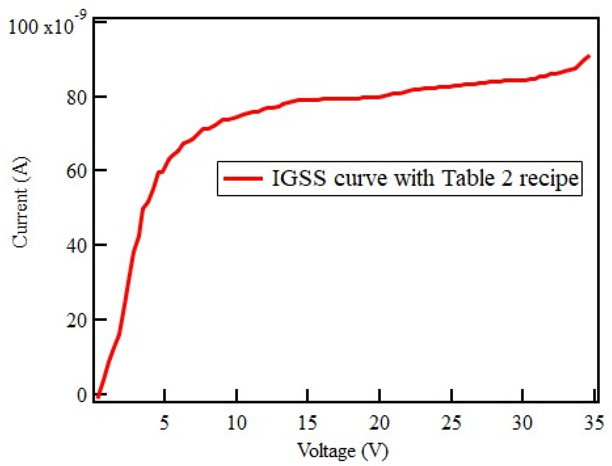
Figure 7 shows the IGSS curve using the etching protocol from Table 2; the slope depicts the IGS value rapidly increasing with a small amount of VGS. However, even with the rising trend, the value of the current stayed below the threshold of 100 nA.
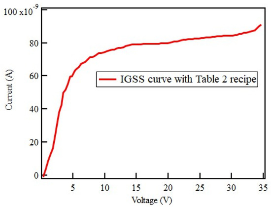
Figure 7.
IGSS curve using the protocol from Table 2 to further investigate gate oxide properties.
Varied reactant gas flow rates and the resulting changes in constituent ratios could also lead to a reduced jagged morphology besides the aforementioned causes. The electronegativity of CHF3 is not strong, helping with sidewall passivation; the effective ratio of CHF3 and SF6 can balance a vertical etching function and sidewall protection that induces uniform sidewalls. The ideal inclination angle of the trench structure is 85–89° in order to match the subsequent deposition of sacrificial oxide and gate oxide. In addition, oxygen is introduced in UV curing steps to react with the C and H polymers generated by etching and attached to the sidewall, which plays a cleaning role.
3.3. Updated Main Etching Protocol
Table 3 shows the updated protocol by changing the main etching parameters; the SF6 gas flow rate was set lower than described in the protocols in Table 1 and Table 2, which helped to further decrease the jagged sidewall morphology.

Table 3.
Etching process parameters by the updated main etching protocol.
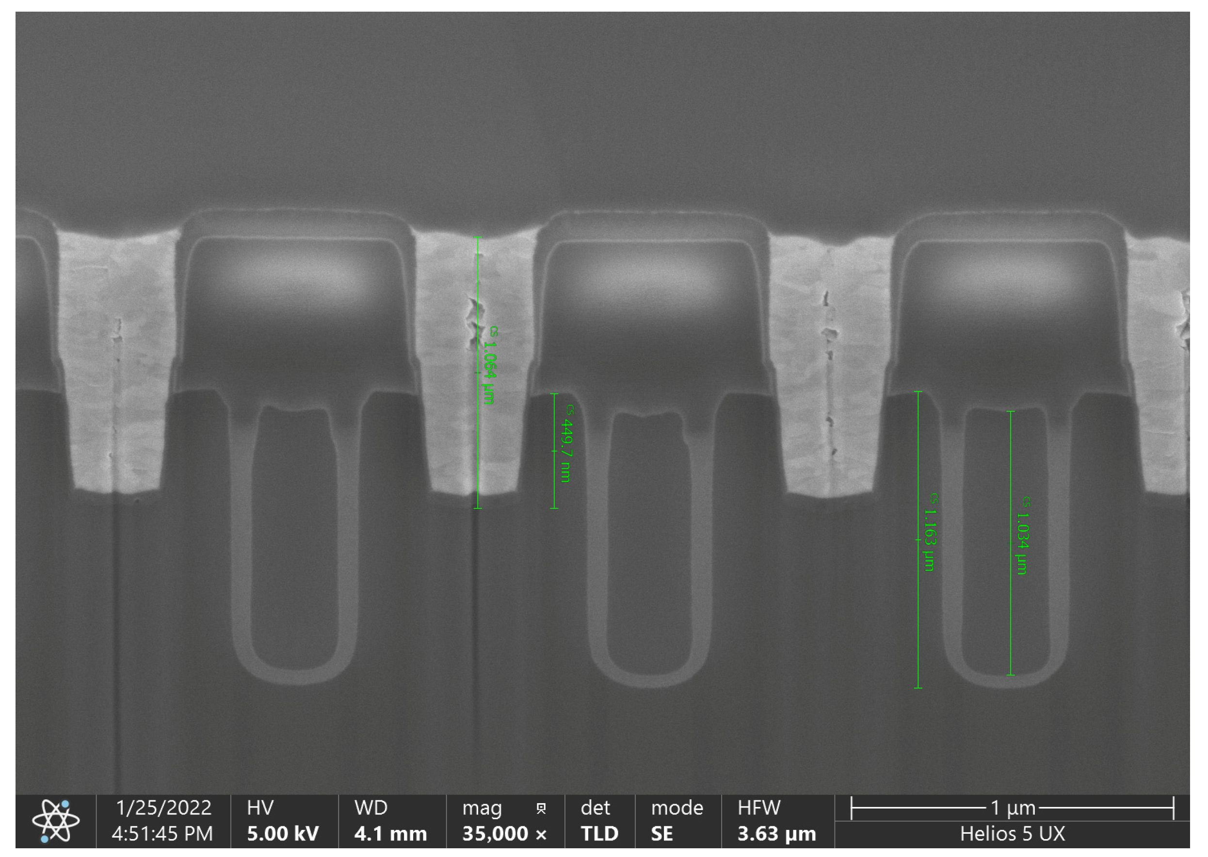
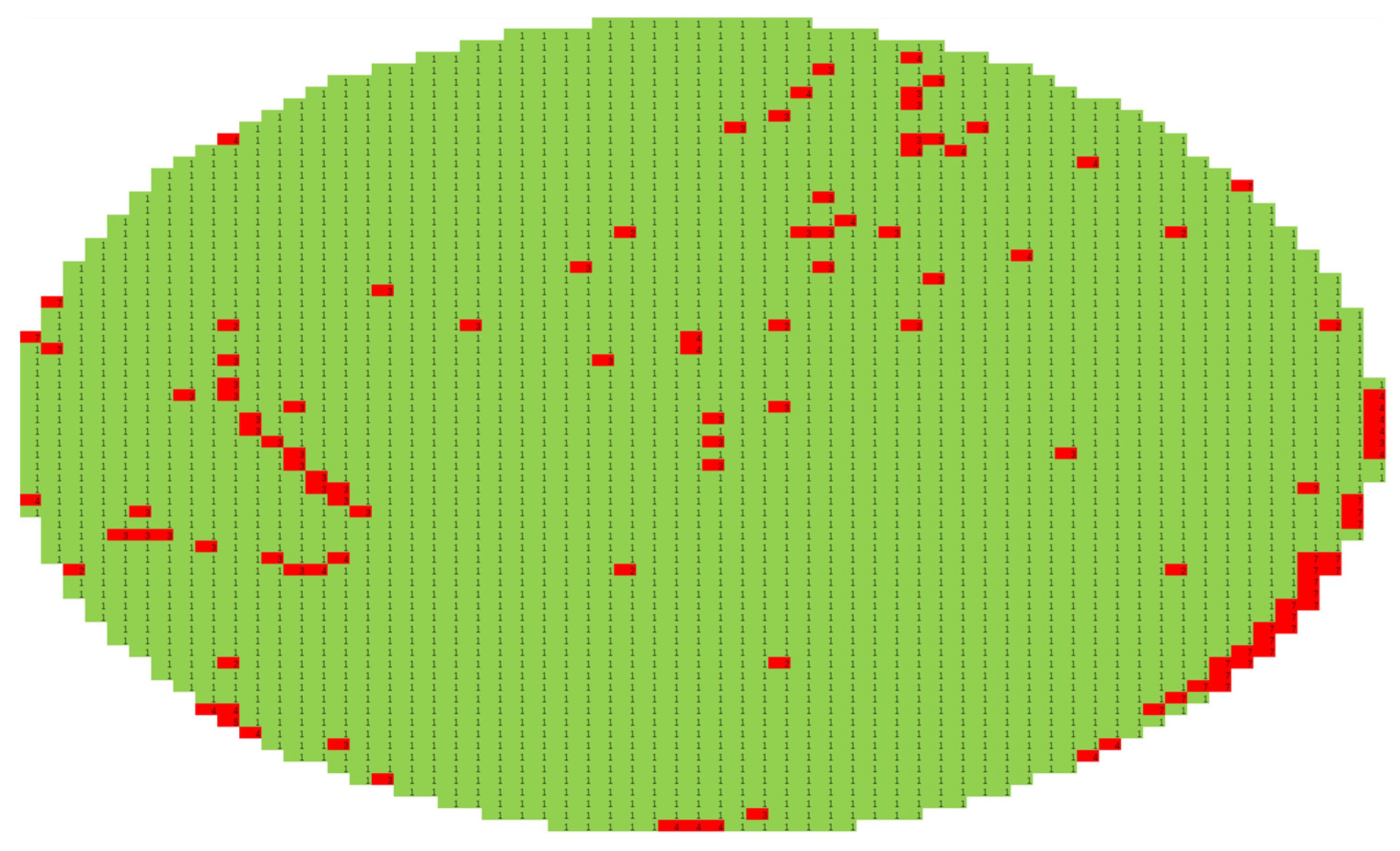
Figure 8a shows the device HRSEM image as a result of using the etching protocol from Table 3, in which the uniformity of the gate oxide was improved with thicknesses around 400 A to 450 A. A threshold thickness of 300 A has been noted to avoid device voltage breakdown, which is well below the thicknesses in our study [20]. The following sequences, such as etching of the rounding steps, the smooth bottom of the sacrifice oxide protocol and the subsequent gate oxide protocol can be optimized to further enhance the uniformity of the gate oxide. The value of the leak current corresponding to the IGSS was evidently lowered with the improvement of the flow process, remaining far below the threshold of 100 nA (Figure 8b). Figure 9 demonstrates the overall bin-map with multiple electrical parameters for the device. Bins that meet the minimum electrical requirements are colored in green. The overall yield of the devices was about 96.5%, which is a large improvement compared to the results in Figures S5 and S6. The failure areas were scattered in a random pattern, unlike the photolithography failure, where the failure areas in the same position across different shots were observed, or etching-related failure, where numerous outer rings were evident.
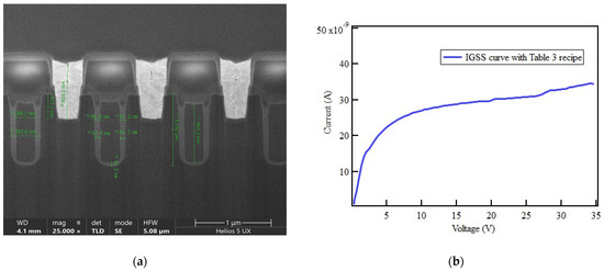
Figure 8.
(a) HRSEM image of the cross section after adding asher and polymer removal processes; (b) IGSS curve using the Table 3 etching protocol.
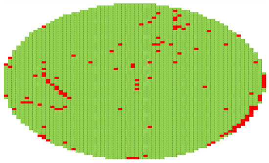
Figure 9.
Bin-map of electrical parameters for the device using the etching protocol from Table 3 (red: failed sample; green: passed sample).
4. Conclusions
Herein, we described an optimization process for the etching trench sidewall profiles of silicon low-voltage devices. The different etching gas protocols showed a sidewall passivation gain improvement with an increased amount of CHF3 and decreased amount of SF6. After adding depolymerization and wet removal of the polymer attached to the etching reaction chamber, the gate oxide uniformity and electrical parameters of the device were significantly improved. The results suggest that UV curing could eliminate the plasma-induced charge accumulation effect, and the wet polymer removal process could reduce the by-products from the etching process. The optimized processes could be applied in trench-structure devices, such as trench photodiodes and trench-isolated LGADs.
Supplementary Materials
The following supporting information can be downloaded at: https://www.mdpi.com/article/10.3390/electronics12112385/s1, Figure S1: TCAD simulation result of Trench mosfet structure (left); net doping concentration of devive (right); Figure S2: The schematic of IGSS (a) and Vth (b) measurement; Figure S3: The microscope-SEM image with repeating experiment by using Table 1 recipe; Figure S4: SEM images of Structure wafers: (a) RF power change; (b) Pressure change; (c) Temperature change; there are no more obvious modification by changing the parameter of RF power, pressure and temperature; Figure S5: bin-map distribution of yield result for the device using initial etching recipe; (red: failed sample; green: passed sample), the overall yield is about 57.27%; Figure S6: bin-map distribution of yield result for the device using updated etching recipe;(red: failed sample; green: passed sample), the overall yield is about 95.29%.
Author Contributions
Methodology, L.J.; software (device simulation), Z.T.; validation, L.C., Z.C., J.F. and W.W.; data curation, L.J. and Z.T.; writing—original draft preparation, L.J.; writing—review and editing, Z.T. and M.Z.; supervision, G.X., J.F., X.G. and M.Z.; funding acquisition, L.J. and J.F. All authors have read and agreed to the published version of the manuscript.
Funding
This research was funded by the Hunan Provincial Science and Technology Department (2022PT1013).
Data Availability Statement
Not applicable.
Conflicts of Interest
The authors declare no conflict of interest.
References
- Vobecky, J.; Vemulapati, U.; Wikström, T.; Boksteen, B.; Dugal, F.; Stiasny, T.; Corvasce, C. Recent Progress in Silicon Devices for Ultra-High Power Applications. In Proceedings of the IEEE International Electron Devices Meeting (IEDM), San Francisco, CA, USA, 11–16 December 2021; pp. 36.34.31–36.34.34. [Google Scholar]
- Williams, R.K.; Darwish, M.N.; Blanchard, R.A.; Siemieniec, R.; Rutter, P.; Kawaguchi, Y. The Trench Power MOSFET: Part I—History, Technology, and Prospects. IEEE Trans. Electron Devices 2017, 64, 674–691. [Google Scholar] [CrossRef]
- Liu, X.; Sun, Q.; Huang, Y.; Chen, Z.; Liu, G.; Zhang, D.W. Optimization of TSV Leakage in Via-Middle TSV Process for Wafer-Level Packaging. Electronics 2021, 10, 2370. [Google Scholar] [CrossRef]
- Wu, B.; Kumar, A.; Pamarthy, S. High aspect ratio silicon etch: A review. J. Appl. Phys. 2010, 108, 051101. [Google Scholar] [CrossRef]
- Laermer, F.; Urban, A. MEMS at Bosch–Si plasma etch success story, history, applications, and products. Plasma Process. Polym. 2019, 16, 1800207. [Google Scholar] [CrossRef]
- Zhang, Z.; Liu, G.; Wang, K. Fabrication of Needle-Like Silicon Nanowires by Using a Nanoparticles-Assisted Bosch Process for both High Hydrophobicity and Anti-Reflection. Micromachines 2021, 12, 1009. [Google Scholar] [CrossRef] [PubMed]
- Rudy, A.S.; Morozov, O.V.; Kurbatov, S.V. A Modernized Bosch Etching Process for the Formation of Tapered Structures on a Silicon Surface. J. Surf. Investig. X-ray Synchrotron Neutron Tech. 2021, 15, 461–466. [Google Scholar] [CrossRef]
- Huff, M. Recent Advances in Reactive Ion Etching and Applications of High-Aspect-Ratio Microfabrication. Micromachines 2021, 12, 991. [Google Scholar] [CrossRef]
- Shi, Z.; Jefimovs, K.; Romano, L.; Stampanoni, M. Towards the Fabrication of High-Aspect-Ratio Silicon Gratings by Deep Reactive Ion Etching. Micromachines 2020, 11, 864. [Google Scholar] [CrossRef] [PubMed]
- Bates, R.L.; Thamban, P.L.S.; Goeckner, M.J.; Overzet, L.J. Silicon etch using SF6/C4F8/Ar gas mixtures. J. Vac. Sci. Technol. A 2014, 32, 041302. [Google Scholar] [CrossRef]
- Amin, T.M.F.; Huda, M.Q.; Tulip, J.; Jäger, W. Sidewall roughness control in deep reactive ion etch process for micromachined Si devices. In Proceedings of the 7th International Conference on Electrical and Computer Engineering, Dhaka, Bangladesh, 20–22 December 2012; pp. 82–85. [Google Scholar]
- Panduranga, P.; Abdou, A.; Ren, Z.; Pedersen, R.H.; Nezhad, M.P. Isotropic silicon etch characteristics in a purely inductively coupled SF6 plasma. J. Vac. Sci. Technol. B 2019, 37, 061206. [Google Scholar] [CrossRef]
- Ng, H.S. Review on Methods for Trench MOSFET Gate Oxide Reliability and Switching Speed Improvement. ECS Trans. 2010, 27, 21–26. [Google Scholar] [CrossRef]
- Madziwa-Nussinov, T.G.; Arnush, D.; Chen, F.F. Ion-Shading Effects During Metal Etch in Plasma Processing. IEEE Trans. Plasma Sci. 2007, 35, 1388–1396. [Google Scholar] [CrossRef]
- Ayesh, M.; Horrocks, A.R.; Kandola, B.K. The Impact of Atmospheric Plasma/UV Laser Treatment on the Chemical and Physical Properties of Cotton and Polyester Fabrics. Fibers 2022, 10, 66. [Google Scholar] [CrossRef]
- Liu, Z.; He, B.; Meng, F.; Bao, Q.; Sun, Y.; Sun, S.; Zhou, G.; Cao, X.; Xin, H. Contact etch process optimization for RF process wafer edge yield improvement. J. Semicond. 2019, 40, 122402. [Google Scholar] [CrossRef]
- Racka-Szmidt, K.; Stonio, B.; Żelazko, J.; Filipiak, M.; Sochacki, M. A Review: Inductively Coupled Plasma Reactive Ion Etching of Silicon Carbide. Materials 2021, 15, 123. [Google Scholar] [CrossRef] [PubMed]
- Lin, Y.; Yuan, R.; Zhang, X.; Chen, Z.; Zhang, H.; Su, Z.; Guo, S.; Wang, X.; Wang, C. Deep Dry Etching of Silicon with Scallop Size Uniformly Larger than 300 nm. Silicon 2018, 11, 651–658. [Google Scholar] [CrossRef]
- Yang, D.; Wang, J.; Li, R.; Ma, Y.; Ma, L. Extremely vertical sidewall trench etching on silicon substrate and modelling etching using artificial neural network. Mater. Res. Express 2019, 6, 125902. [Google Scholar] [CrossRef]
- Lombardo, S.; Stathis, J.H.; Linder, B.P.; Pey, K.L.; Palumbo, F.; Tung, C.H. Dielectric breakdown mechanisms in gate oxides. J. Appl. Phys. 2005, 98, 121301. [Google Scholar] [CrossRef]
Disclaimer/Publisher’s Note: The statements, opinions and data contained in all publications are solely those of the individual author(s) and contributor(s) and not of MDPI and/or the editor(s). MDPI and/or the editor(s) disclaim responsibility for any injury to people or property resulting from any ideas, methods, instructions or products referred to in the content. |
© 2023 by the authors. Licensee MDPI, Basel, Switzerland. This article is an open access article distributed under the terms and conditions of the Creative Commons Attribution (CC BY) license (https://creativecommons.org/licenses/by/4.0/).


