1. Introduction
Modern phase array systems are heavily reliant on phase shifters for adaptive beam forming and steering. They are utilized in both the transmit and receive path, to provide the necessary insertion phase to the antenna elements of the array. A large number of phase shifters are employed to realize a single system, as continuous and fast beam scanning in both azimuth and elevation is required along with adaptive main lobe and null placements. Therefore, considerable efforts have been made to: (1) reduce the size of the phase shifters, as the number of antenna elements in a typical antenna array is large, and the available space is limited; (2) achieve a lower insertion loss, as the transmit power and noise figure of the phased array is directly affected by the loss of the phase shifter; and (3) achieve a minimum phase variation and larger operating bandwidths, as the beam forming accuracy is highly dependent on the phase shift accuracy [
1].
The literature reports various topologies of phase shifters Including both active [
2] and passive designs [
3]. Active phase shifters are design in conjunction with amplifiers and provide continuous variation of phase; however, they consume a large amount of DC power and have complex circuitry. On the other hand, passive phase shifters have low power consumption, high linearity and are inherently bi-directional in nature, thus offering significant advantages compared to active designs [
4]. The most commonly used passive phase shifters are switched-type [
5,
6], loaded-line-type [
7,
8] and Reflection-Type Phase shifters (RTPS) [
9,
10,
11]. However, an N-bit phase shifter is traditionally implemented by cascading multiple 1-bit structures, which not only leads to larger dimensions but also incurs higher insertion loss and accumulated phase errors.
In conventional switched-line multi-bit phase shifters, delay lines of varying lengths occupy a large area. In addition, the insertion loss is higher due to the high number of single-pole double-throw (SP2T) switches used, which are connected in-line to the transmission lines. The switches are generally made up of p-i-n diodes, metal semiconductor field effect transistors (MESFETs) or high-electron-mobility transistors (HEMTs). To reduce the losses, solutions employing SP2T and single-pole four-throw (SP4T) switches [
12,
13] based on microelectromechanical system (MEMS) technology have been reported. However, the size, endurance rating and low switching speeds of the MEMS switches are still considered as key limitations in their practical deployment.
Multi-bit loaded-line and distributed phase shifters have a large footprint because the phase-shifting elements (open or short-circuited stubs) need to be spaced apart by a quarter-wavelength [
14,
15] on a transmission line. In addition, the phase shift range is limited, and they are not commonly used when the required phase shift is more than 45°. As a good alternative, RTPS [
16,
17] offers good input/output matching with simple control and large phase tuning ranges. They are usually constructed using a four-port coupler (usually the 3-dB branch line coupler) and two identical tunable reflective loads (commonly a varactor diode) to achieve the desired phase shifts. RTPS solutions does not offer much flexibility in terms of dimensions, as the bulky 3-dB coupler requires a large area. This becomes especially critical in multi-bit RTPS implementations [
18,
19]. Furthermore, the bandwidth of the RTPS is dependent on the characteristics of the 3-dB coupler, and the reflective loads and traditional implementations offer limited bandwidths. Lumped elements couplers [
20] have been used to reduce the size, but they suffer from even narrower bandwidths. Coupled-line couplers [
21] have been used to enhance the bandwidths, but they require very small gaps between the coupled strips, which are difficult to fabricate using standard PCB fabrication process. Foregone in view, it is therefore relevant to investigate multi-bit phase shifters from the view point of dimensions while achieving a lower insertion loss and good phase accuracy.
The novel concept of single-unit multi-bit phase shifters was presented by the authors using the inverted-E topology [
22]. A single Main Transmission Line (MTL) was loaded with multiple pair of three open-circuited stubs to achieve the desired phase shifts. A highly compact single-unit 3-bit phase shifter with lower insertion loss was presented and demonstrated; however, the phase shift range was limited up to 90° due to the band-stop effect generated by the loaded open-circuited stubs.
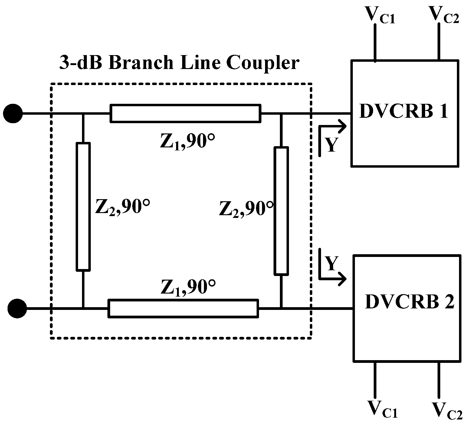
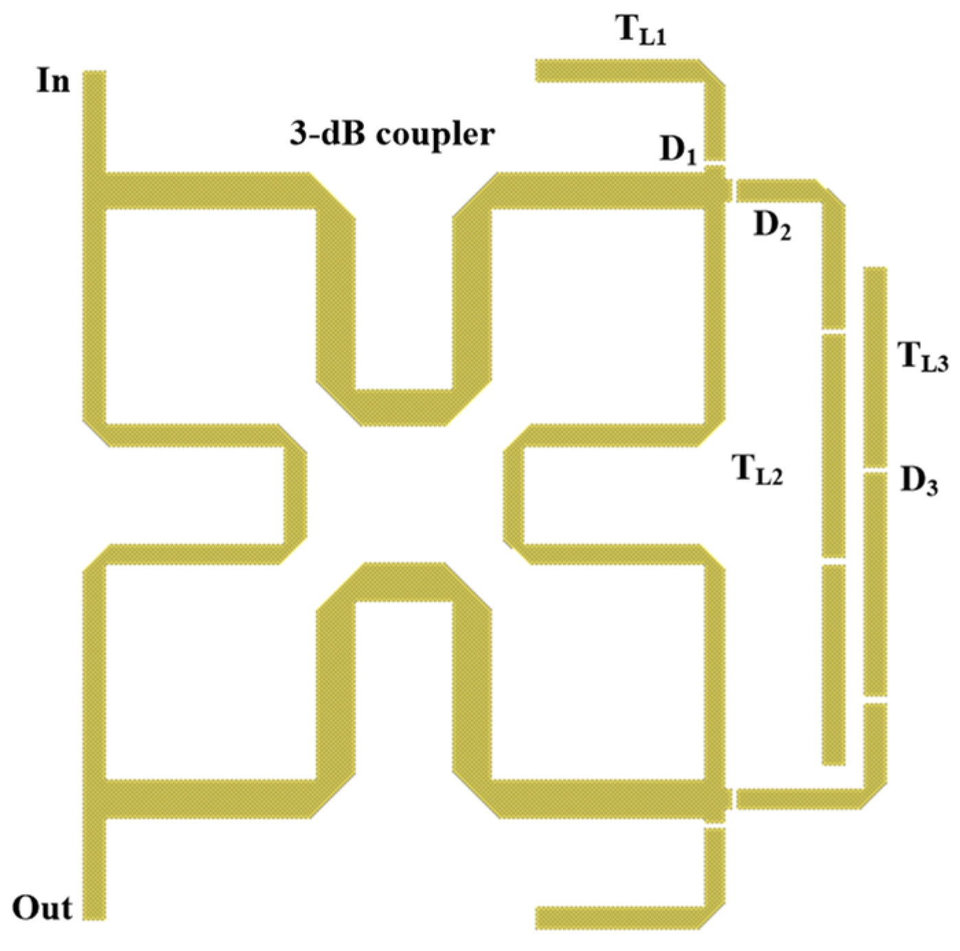
To enhance the phase shift range up to 180° and beyond, while maintaining compact dimensions using a single-unit structure, this work presents single-unit two-bit reflection-type phase shifters (SUTBRTPSs). Unlike the traditional multi-bit RTPS solutions, herein, only one 3-dB hybrid coupler is utilized to achieve two-phase shift bits, as shown in
Figure 1. The simple geometry comprises a quarter-wavelength 3-dB branch line coupler and two identical dual-voltage controlled reactance blocks (DVCRBs), each with an input susceptance of
Y, loaded to the through and coupled ports of the coupler. Each DVCRB comprises three open-ended transmission lines and switching p-i-n diodes. The open-circuited transmission lines provide the needed susceptance to achieve half of the desired phase shift. When individual stubs of the two DVCRBS are loaded simultaneously using a single control voltage, the combined loaded susceptance generates the required phase shift between the input and isolated port of the coupler. The proposed SUTBRTPS offers several advantageous features such as highly compact dimensions, lower insertion loss, large phase shift range and good phase accuracy. Additionally, they can be easily fabricated using standard PCB fabrication technology.
2. Design Methodology
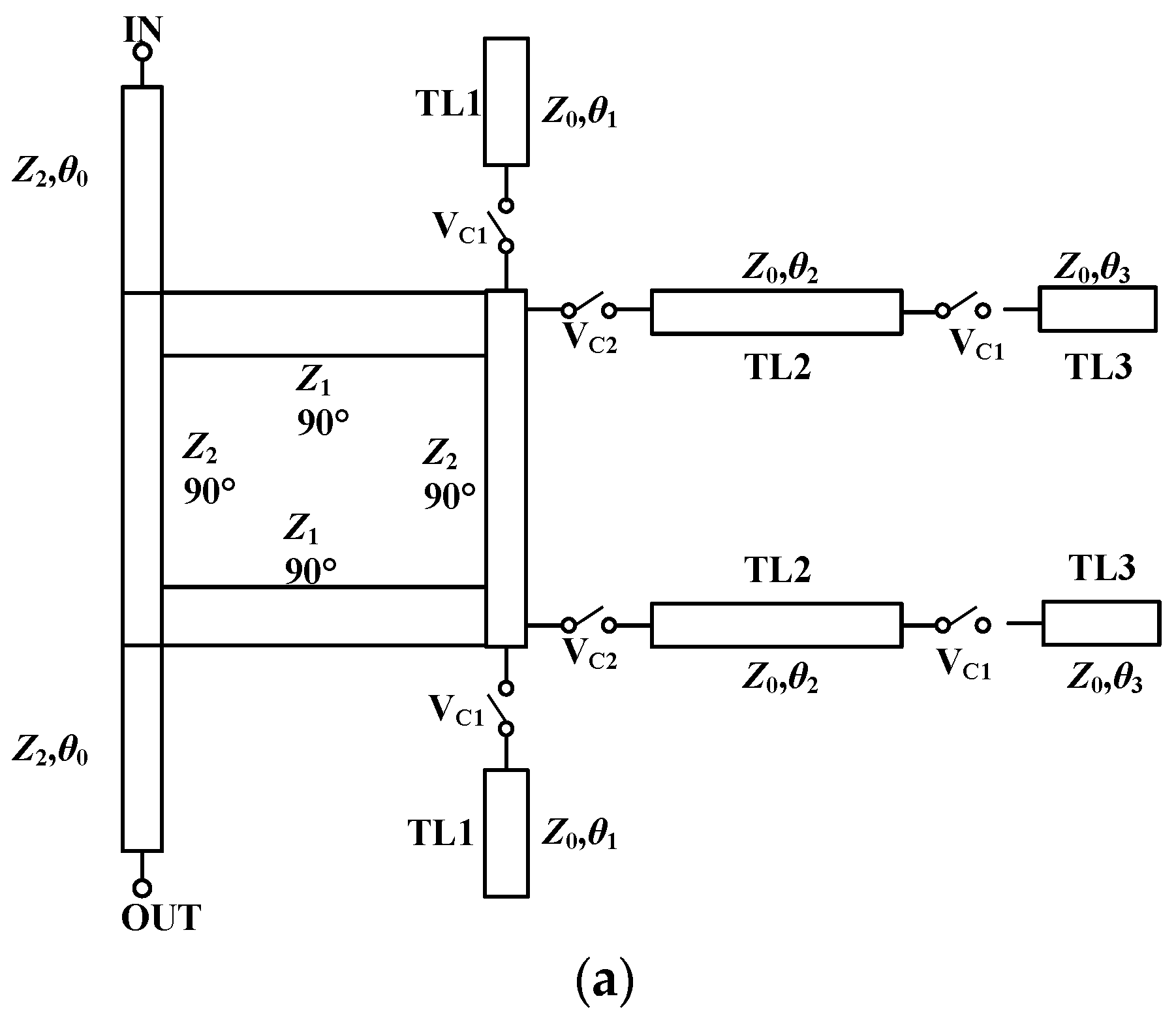
Figure 2a shows the circuit configuration of the proposed SUTBRTPS. It comprises a typical quarter-wavelength 3-dB branch line coupler, with
Z2 =
Z0 and
, where
Z0 is the input/output port impedance. Each DVCRB consists of three open-ended transmission lines, with the following characteristics: impedance of
Z0 = 50Ω and electrical lengths of
,
and
, respectively. The two identical DVCRBs are selectively loaded to the 3-dB coupler using two control voltages,
VC1 and
VC2. Each DVCRB provides the needed susceptance to generate half of the required phase shift and is equivalent to an open-circuited transmission line, with the following characteristics: impedance of
Z0 and electrical length of
, as shown in
Figure 2b; here,
is the required electrical length corresponding to a desired phase state.
To explain the design methodology, let us represent the phase shifts bits of the SUTBRTPS as
φ1 and
φ2. When control voltages
VC1 and
VC2 are both zero, the input susceptance of the loaded DVCRBs is infinity, and the circuit is in its OFF state. This state can be represented by
, and the equivalent electrical length for the open-circuited condition is:
When control voltage
VC1 is applied, the transmission line, labeled as
TL1, having a characteristics impedance of
Z0 and electrical length of
, is loaded to the coupler. The phase state can be represented as
, and the desired phase shift, equivalent to the electrical length of the
TL1 is generated as:
When control voltage
VC2 is applied, the transmission line, labeled as
TL2, having a characteristics impedance of
Z0 and electrical length of
, is loaded to the coupler. The phase state can be represented as
, and a phase shift equivalent to the electrical of
TL2 is generated as:
Finally, when both the control voltages
VC1 and
VC2 are simultaneously applied, the circuit is equivalent to the parallel combination of two open-circuited transmission lines having electrical lengths of
and
, respectively. The phase state can be represented as
, and the combined loaded susceptance generates a phase shift equal to:
The required electrical lengths of
and
can be easily computed according to the required phase shifts bits values. To compute the required electrical length
, as shown in
Figure 2b, the input susceptance of
TL1 can be written as:
Likewise, the series circuit of
TL2 and
TL3 is equivalent to an open-circuit transmission line with an electrical length equal to
, and its input susceptance can be written as:
Considering the equalization in loaded susceptance at the loaded port
By solving (7), we obtain
Consequently, the electrical length
can be calculated as
To validate the proposed design theory, here, we take the example of two typical SUTBRTPSs with
= 45°,
= 90° and
= 22.5°,
= 180°, respectively, at 1 GHz. The four phase states are 0/45°/90°/135° and 0/22.5°/180°/202.5°, respectively. The required phase shifts of each phase state are listed below
Subsequently, the required electrical lengths for each phase state can be computed using Equations (2), (3) and (8) and are given below
If the theoretical value of the electrical length is computed to a negative value, the electrical length value should be redefined according to the periodicity of the trigonometric function.
Similarly, with
= 22.5° and
= 180°, the required phase shifts of each phase state are
The required parameter values at 1 GHz are then computed as
3. Simulations, Fabrication and Measurements
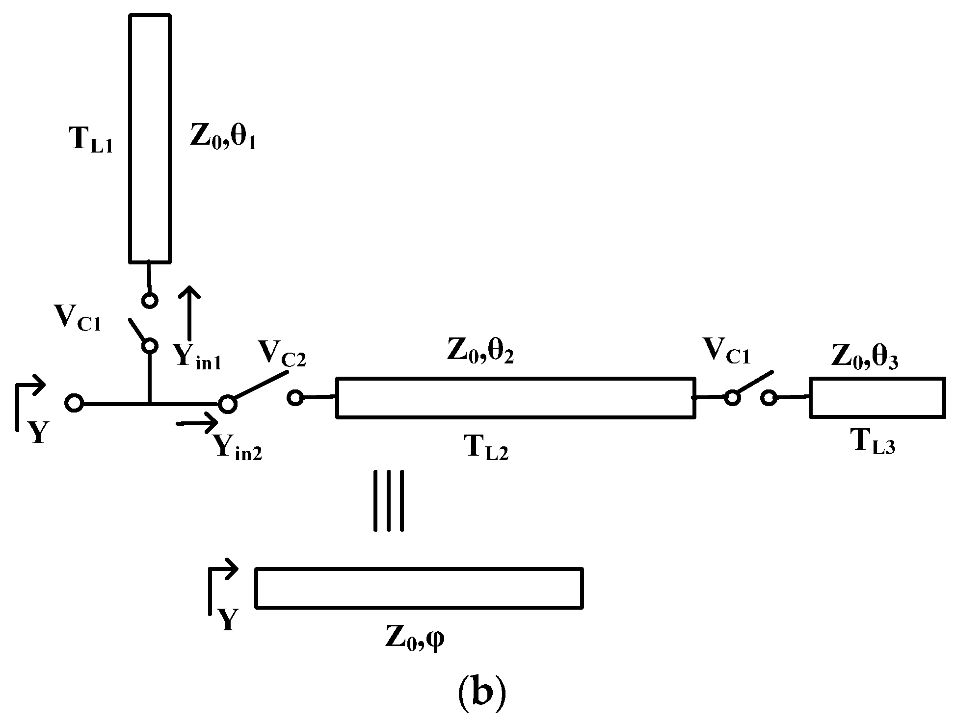
For validation of the proposed theory, full-wave momentum simulations were carried out using Agilent Advance Design System (ADS). The effects of the switching p-i-n diodes on the phase shift was compensated by fine-tuning the electrical lengths of the transmission lines using the manufacturer-provided data. For demonstration, the proposed SUTBRTPSs (45°/90° and 22.5°/180°), centered at 1 GHz, are fabricated on Rogers 4003C substrate, with a dielectric constant of 3.55 and thickness of 0.508mm. P-i-n diodes (model # SMP1331-087LF from Skyworks) having a junction capacitance of 0.27 pF and a minimum resistance of 2.7 Ω in forward-biased conditions are utilized for switching. The optimized layout of the proposed SUTBRTPS is given in
Figure 3, and the synthesized parameter values are listed in
Table 1.
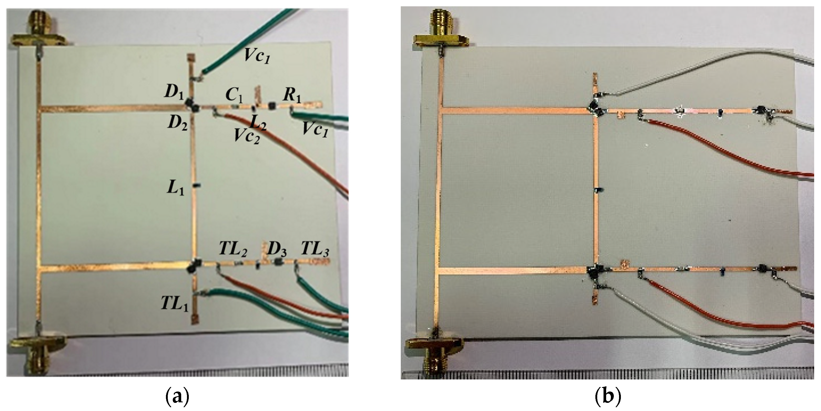
The photographs of the two fabricated designs are shown in
Figure 4a,b, respectively. Herein, inductors
L1 and
L2 (100 nH) are used to ground the overall circuit, whereas
R1 = 1 KΩ is a current-limiting resistor used to bias the diodes, whereas the capacitor,
C1 = 100 pF, is used to isolate DC from the RF signal. A control voltage of 0/3 V is used to put the diodes in forward- and reversed-biased conditions.
The overall dimensions of the fabricated designs, including the SMA connectors, are and , respectively, which are significantly smaller compared to traditional multi-bit RTPS solutions using multiple cascaded phase-shifting units. Moreover, being the main contributing factor to the overall size of the proposed SUTBRTPS, the size of the 3-dB hybrid coupler can be further reduced by using meandered/folded lines. Likewise, the transmission lines of the DVCRBs can also be used in a folded configuration.
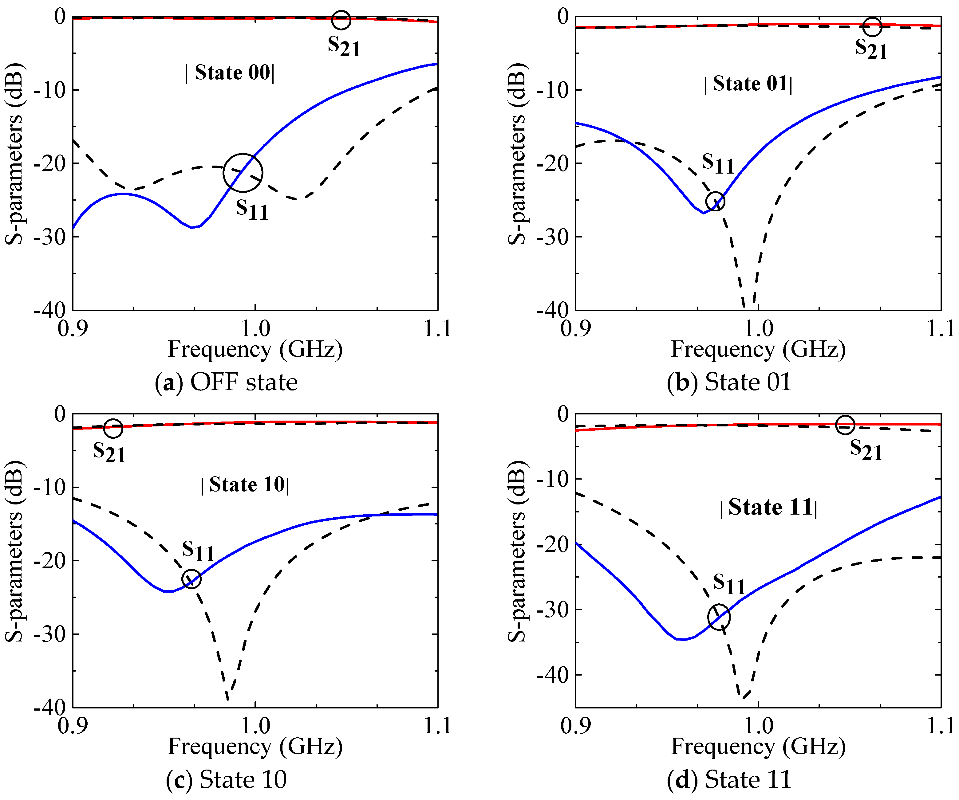
To validate the performance of the fabricated designs, two port S-parameters measurements were performed using a network analyzer (Model # N5235A from Keysight). A comparison between the simulated and measured magnitude and phase response of the 45°/90° SUTBRTPS is shown in
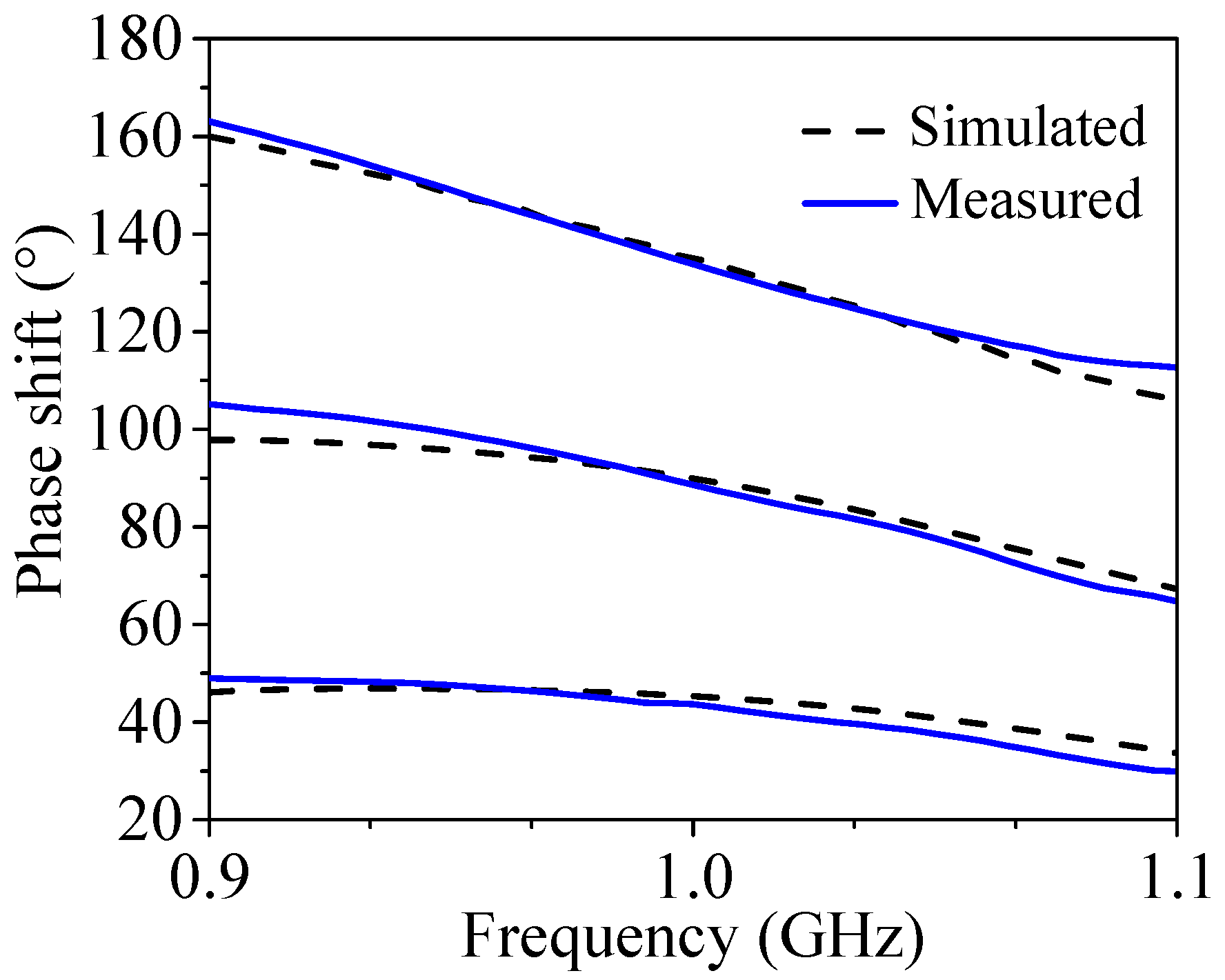
Figure 5 and
Figure 6, respectively.
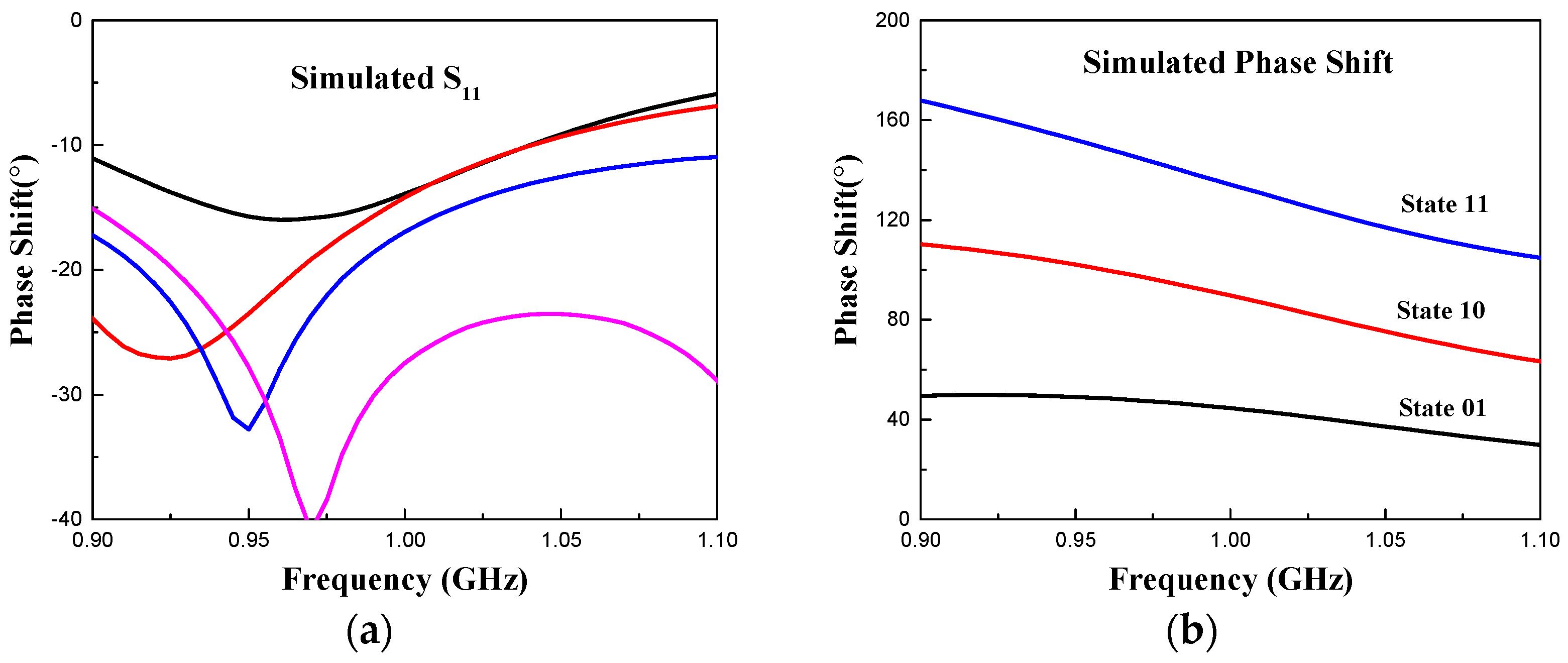
As shown in
Figure 5a–d, the measured return loss at the center frequency of 1 GHz is better than 20 dB for all four phase states, whereas the maximum insertion loss of 1.7 dB is measured for phase state 11. It is important to note that for state 11, all the six p-i-n diodes are in forward-biased condition, and the two DVCRBSs are fully loaded to the coupler. The insertion losses for phase states 00, 01 and 10 are 0.19 dB, 1.2 dB and 1.3 dB, respectively. The amplitude variation is less than 0.5 dB in the operating frequency band.
As depicted in
Figure 6, the measured phase shifts at the center frequency are 44.7°, 89.6° and 133.9°, respectively. The maximum phase shift error of 1.1° is observed for phase state 11. The achieved phase shift is accurate at the center frequency; however, the phase variation vs. frequency is observed to be on the higher side but still similar to that achieved through traditional 1-bit RTPS solutions. The phase response of the RTPSs is mainly attributed to the frequency performance of the coupler and the loaded reactance. Being inherently narrow band in nature, the phase flatness using the traditional 3-dB quarter-wave coupler is poor. To circumvent this problem, coupled-line couplers and Lange couplers may be investigated as possible solutions, at the expense of circuit complexity. It is also pertinent to note that phase measurements are more prone to fabrication tolerances and measurement inaccuracies.
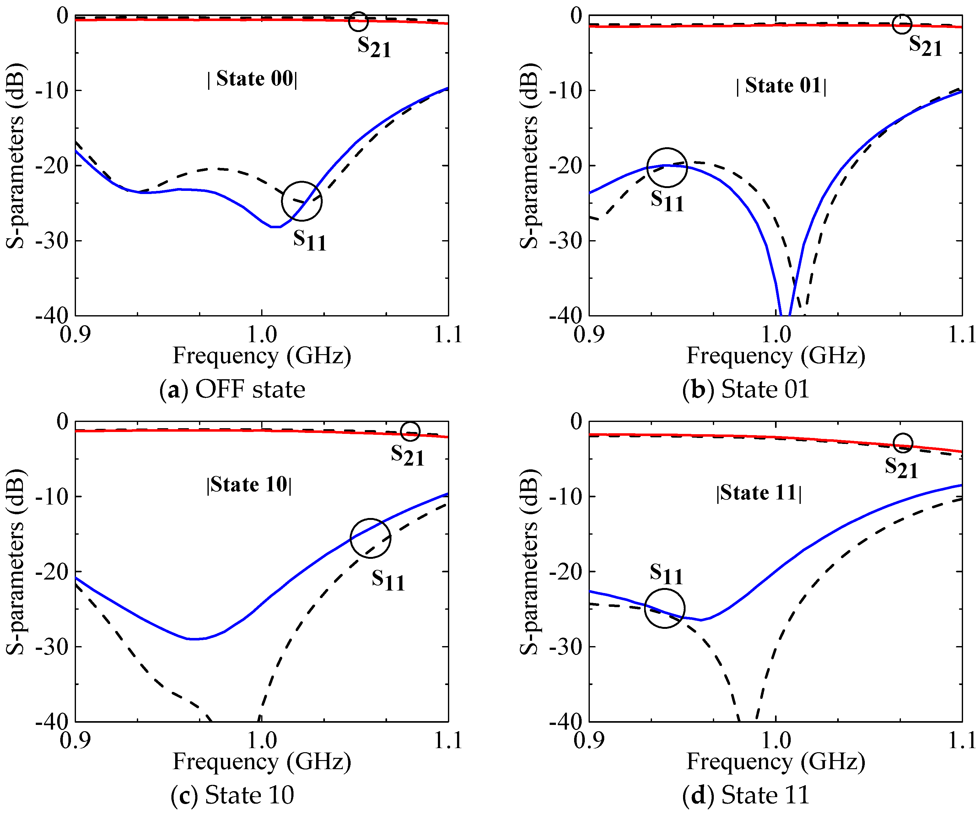
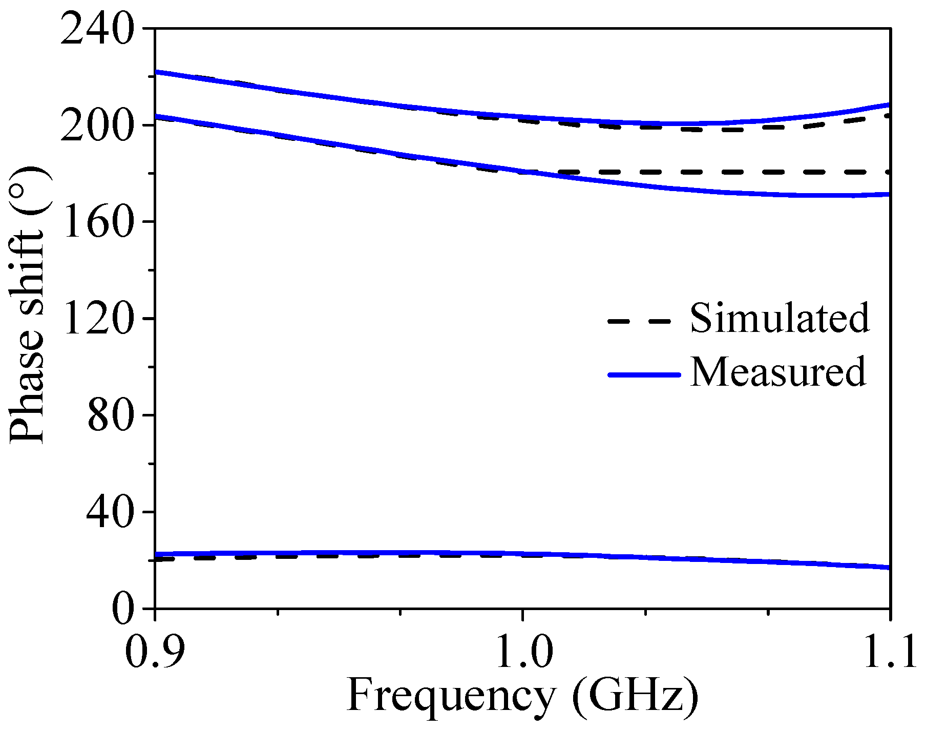
The magnitude and phase shift response of the 22.5°/180° SUTBRTPS are shown in
Figure 7 and
Figure 8, respectively.
It can be seen from
Figure 7 that the measured return loss is better than 20 dB for all phase states, and the maximum measured insertion loss of 2.1 dB is observed for phase state 11. However, for phase states 00, 01 and 10, the measured insertion losses are 0.19 dB, 1.3 dB and 1.2 dB, respectively. The amplitude variation across the frequency band is less than 0.7 dB.
As depicted in
Figure 8, the measured phase shifts at the center frequency are 22.6°, 180.8° and 203.3°, respectively. The maximum phase error, at center frequency, of 0.7° is observed for phase state 11. Moreover, a slight mismatch is observed for larger phase states 10 and 11, which can be attributed to the requirement of higher susceptance values, requiring the use of longer transmission lines, which results in higher slopes of susceptance curves.
The measured results are consistent with the simulation results and validate the design theory. A very good magnitude response is observed with a lower insertion ranging from 0.2 to 2.1 dB and a minimum amplitude variation across the design frequency band. In addition, accurate phase shift is achieved at the center frequency; however, the phase flatness is similar to that of typical RTPS solutions, with a narrow operating bandwidth of 40 MHz. This is mainly attributed to the frequency characteristics of the coupler and the loaded reactance blocks. To enhance the bandwidths of the proposed SUTBRTPS, a coupled-line coupler may provide a possible solution.
The main advantage offered by the proposed design is compact dimensions, as only one hybrid coupler is used instead of multiple cascaded structures of the traditional multi-bit RTPS solutions. In addition, a lower insertion loss with a large phase shift range of 180° is achieved.
In order to further reduce the size of the proposed SUTBRTPS, folded and meandered lines can be used instead of uniform transmission lines, as shown in
Figure 9. The size of the proposed model using meandered lines for the 45°/90° SUTBRTPS is
, which corresponds to almost 50% size reduction compared to the circuits shown in
Figure 4. Although the design is not fabricated and measured, the circuit model is optimized, and full wave momentum simulations were carried out to compare the results with those achieved by the fabricated designs. As shown in
Figure 10, the return loss is better than 10 dB in the whole operating band, and the phase shifts at the center frequency are 44.6°, 89.7° and 134.2°, respectively.
Finally,
Table 2 presents a comparison between the proposed SUTBRTPSs and other state-of-the-art solutions. In comparison to the loaded-line phase shifters, the dimensions are many times smaller, and the phase shift range is larger, whereas for 45° and 90° phase shifts, the insertion loss is comparable.
Compared with the switched-type multi-bit phase shifters, compact dimensions and lower insertion losses are observed. A high-pass/low-pass configuration [
23] has larger dimensions, as multiple filter sections are employed, and requires four diodes per bit; hence, the insertion loss is higher. In comparison to the multi-bit RTPS solutions, the proposed SUTBRTPS achieves much smaller sizes as only one 3-dB hybrid coupler is used, whereas the insertion loss is also lower. Accurate phase shift is observed at the center frequency; however, the operating bandwidth is narrow, and the phase variation is high; however, the reported bandwidth [
18] is 25 MHz, and the phase error and variation in [
16] is greater than 3° and 7°, albeit over a wider operating frequency band. It can therefore be concluded that with traditional quarter-wavelength couplers, the operating bandwidth of the RTPSs is narrow, and the phase variation is high. Similarly, compared to our previous work, the circuit geometry is sufficiently succinct as the number of stubs and switches are significantly reduced; moreover, a larger phase shift range has been achieved.


