Article

Noise Reduction of Atomic Force Microscopy Measurement Data for Fitting Verification of Chemical Mechanical Planarization Model

1
The EDA Center, Institute of Microelectronics, Chinese Academy of Sciences, Beijing 100029, China
2
The School of Electronic, Electrical and Communication Engineering, University of Chinese Academy of Sciences, Beijing 100049, China
*
Author to whom correspondence should be addressed.
Electronics 2023, 12(11), 2422; https://doi.org/10.3390/electronics12112422
Submission received: 25 April 2023 / Revised: 19 May 2023 / Accepted: 23 May 2023 / Published: 26 May 2023

Abstract

:
In advanced integrated circuit manufacturing processes, the quality of chemical mechanical flattening is a key factor affecting chip performance and yield. Therefore, it has become increasingly important to develop an accurate predictive model for the chip surface topography after chemical mechanical flattening. In the modeling process, the noise problem of atomic force microscopy measurement data is relatively serious. To solve this problem, the noise characteristics of atomic force microscope measurement data for chip surface topography in this field are studied and discussed in this paper. It is found that the noise present in such problems is mainly triggered by the vibration and tilt of the probe. Two types of noise, low-frequency and high-frequency, are presented in the time domain. In order to solve the noise problem in this modeling data, this paper analyzes the spectral characteristics of the measurement data using Fourier transform, and a wavelet-Fourier transform composite noise reduction process is proposed. The algorithm is applied to the noise reduction of the chip surface data of 32 nm copper interconnect process. The noise reduction results were compared with scanning electron microscope photographs to verify the effectiveness of the noise reduction.

1. Introduction

Because of the increased complexity of integrated circuit manufacturing, process tolerance requirements are becoming increasingly stringent. Chemical mechanical planarization (CMP) is a primary planarization technology in process manufacturing in which the surface morphology of the chip after planarization directly influences the yield and electrical properties of the circuit [1,2,3,4,5,6]. Therefore, models for predicting post-CMP chip morphology are gaining significant attention in chip design validation, equipment development, and process development [7,8,9,10]. In CMP modeling, the surface morphology measurement quality of the actual tapeout data is directly related to final model precision, because the measurement data are involved in critical links, such as parameter adjustment, validation, and final model testing, excluding mechanism research. Atomic force microscopy (AFM) is a widely used method for measuring the microscopic morphology of the chip surface, such that denoising the AFM measurement data has become crucial in ensuring CMP modeling accuracy.
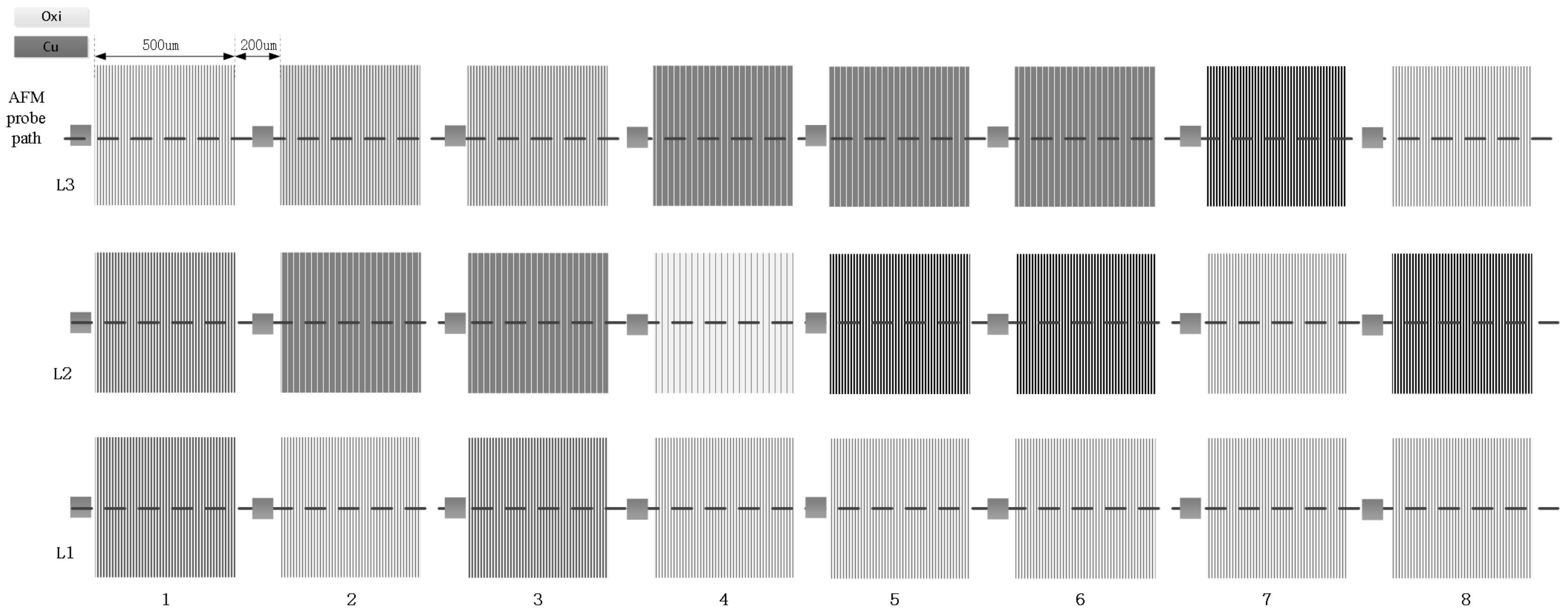
The morphology measurement data required for die-scale CMP modeling are obtained through the “layout design–tapeout–AFM measurement” process. The layout design for CMP modeling typically has a trench structure [11,12], whose design parameters and morphology characterization are shown in Figure 1. The tip of the AFM probe glides over the wafer surface and records the morphology along its trajectory under gravity. Our tapeout layout structure and AFM measurement tracks are shown in Figure 2. The graphical parameters of the trench array are listed in Table 1. The SIMC 32 nm Cu interconnection tapeout is designed to establish and validate the CMP morphology prediction model for the 32 nm Cu interconnection.
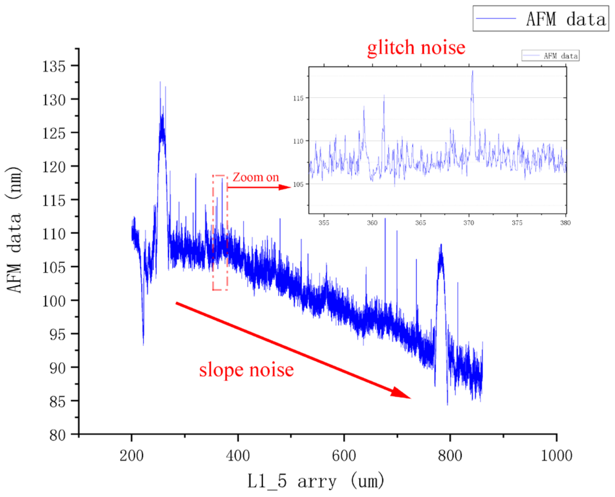
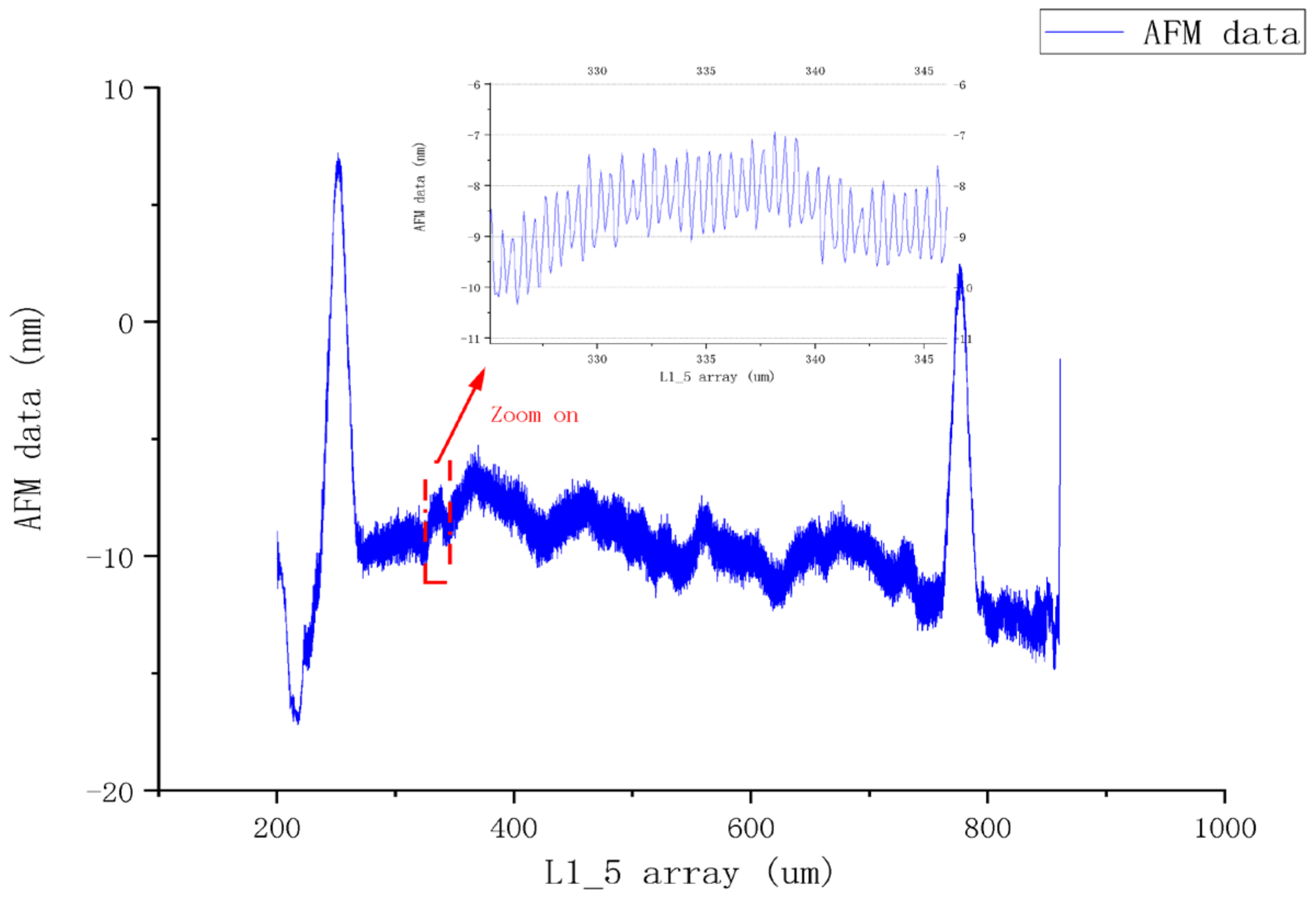
Figure 3 shows the details of an AFM morphology dataset, where glitch and slope noise occur. These severely affect the morphology dishing measurements, including the parameter fitting and validation of subsequent modeling. According to previous studies, AFM noise may be caused by several factors. AFM noise can be caused by electrical disturbances in the measurement equipment, disturbances in the measurement environment [13], and probe mechanical vibration. The noise generated by different mechanisms and the corresponding noise frequency characteristics are presented in [14], which provides the basis for the analysis of noise using spectral characteristics in the later part of the paper. From this, we can infer that the noise appearing in this experiment belongs to the mechanical noise generated by probe mechanical vibration.
When an AFM probe tip passes over the surface to be measured, mechanical vibration and tilting inevitably occur. This generates glitch and slope noise in AFM data. In previous studies [15,16,17], the noise was eliminated via multiple repeat tests or optimized measurements using the AFM equipment. This technique functions effectively but is complicated for researchers who lack expertise in using AFM equipment, and requires measurements with other tissues. To address this surface data measurement problem, we attempted to apply digital signal processing to minimize noise in the AFM data.
Slope noise, predominately with low frequencies, is relatively easy to discard. With a presumably fixed slope angle, slope noise can be eliminated by vertically correcting (planarization) the data after applying a sample rigid-registration method. However, glitch noise is more difficult to remove than slope noise because the former requires nonrigid registration for correction. Yi et al. [18] developed a finite impulse response-based feedforward control approach to mitigate acoustic-caused probe vibration during AFM imaging. Jones et al. [14] presented a nonrigid registration method based on the gradient descent technique. Wu [19] proposed an approach for the automated vertical drift correction of AFM images based on morphology prediction. Both could correct the image distortion; however, computational efficiency is very important. As the AFM data are used for CMP model validation, the pixel-by-pixel correction of noise in the data is a luxury. We aimed to develop an efficient data noise-reduction algorithm to minimize computation effort while maintaining the local shape.
Our initial approach was to adopt the frequency characteristics of the target data to denoise the AFM data. Because the layout design has a trench structure—a regular periodic structure—the post-CMP surface morphology is supposedly periodic. It has its own specific frequency. Accordingly, a low-pass filter was designed to perform low-pass noise reduction on the AFM data. However, this led to a failure owing to the innate characteristics of the measured AFM data, with its complex frequency components and varied energy distribution at different frequencies. Meanwhile, the post-CMP morphology exhibited nanoscale fluctuations (dishing or erosion), which were close to the Nyquist sampling frequency [20,21] in the AFM measurement. The target morphology measurement data were high-frequency; hence, it was difficult to achieve precise filtering with low- or band-pass filters. The specific data characteristics are described in Section 3. After multiple trials, we used the technique developed in [22], and formulated a composite Wavelet transform–Fourier transform (WT–FT) filtering technique that could effectively discard glitch noise and restore the surface morphology of the test chip. In addition, its denoising effectiveness was verified in comparison with the cross-section data obtained using scanning electron microscopy (SEM).
The remainder of this paper is organized as follows. Section 2 introduces the relevant Fourier transform (FT) and Wavelet transform (WT) principles and analyzes the characteristics of the AFM data noise, including the advantages and disadvantages of both methods used for noise reduction. Section 3 presents the workflow of a novel denoising algorithm that sequentially applies WT and FT in analyzing and reducing AFM data noise, followed by a demonstration of the actual denoising results of the algorithm. The data analysis and discussion are presented in Section 4, and the conclusion and outlook are summarized in Section 5.

2. FT and WT

2.1. FT

Because AFM data are energy signals, that is, a set of one-dimensional AFM data f(x), they belong to L(R2) space, and can be approximated in the Fourier [23] series (Equation (1)):
f ( x ) n a n Γ n ( x ) ( n Z )
Here, Γ n ( x ) ( n Z ) is the Fourier basis function, and a n is a Fourier coefficient representing the projected coordinates or energy distribution of the original signal f(x) on a series of Fourier bases. FT is the process of calculating the Fourier coefficients, or energy distribution, of the original signal f(x) on the Fourier basis of different frequencies. Because of the orthogonality (Equation (2)) of the Fourier basis, the Fourier coefficients can be calculated using Equation (3), that is, the FT.
Γ m ( x ) , Γ n ( x ) = 1 ( m = n ) 0 ( m n )
a n = f ( t ) , Γ n ( x )
Using FT, researchers can analyze the frequency components of signals from the perspective of the frequency domain, and process the frequency domain signals via signal frequency screening or thresholding to discard the signal noise. However, all time domain information is lost after FT despite its excellent frequency domain resolution, triggering several problems in actual nonstationary signal processing. For instance, one cannot determine whether the low-frequency components in the frequency domain signals originate from the measurement structure or unexpected measurement deviations. In several cases, the denoising results of AFM data must be qualitatively confirmed by the human eye, in which case time domain information becomes part of the denoising evaluation and cannot be discarded. To address this problem, we introduced the WT to further analyze AFM data.

2.2. WT

Similar to FT, WT computes the projection coefficients on the corresponding wavelet bases of the function. However, unlike the Fourier basis, in addition to exhibiting orthogonality at different frequencies, a series of discrete wavelet bases φ a , b ( x ) a , b Z also have time parameters such that the wavelet bases at different times are orthogonal to each other, as expressed by Equation (4). φ ( x ) , which is the mother wavelet function, and its FT satisfy Equation (5); in addition, its relationship with discrete wavelet bases satisfies Equation (6).
φ a , b ( x ) , φ m , n ( x ) = 0   ( a m   o r   b n ) 1               e l s e
φ ( x ) L 2 ( R ) , R Ψ 2 ( w ) w < +
φ a , b ( x ) = 1 a φ ( x b a )           ( a , b Z )
Based on the WT, Mallat [24] proposed a multiresolution analysis, presented in [18], where a scaling function ϕ ( x ) was introduced. Fast calculation and visualization of discrete dyadic wavelet decomposition were achieved. Similar to the Fourier series, energy signal can be expressed as follows.
f ( x ) = n c L , n ϕ L , n ( x ) + l = 1 L n d l , n φ l , n ( x )
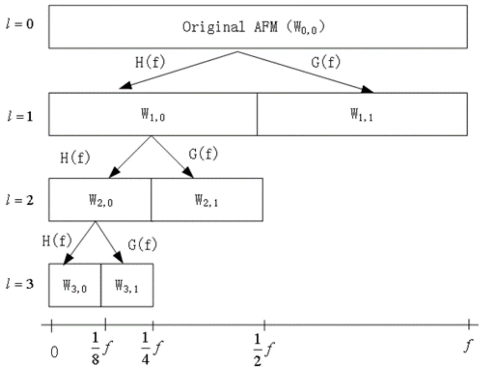
Discrete WT (DWT) is the process of calculating wavelet coefficients, c L , n and d l , n . Based on the description in [25], the Mallat fast algorithm process is illustrated in Figure 4. The Mallat multiresolution analysis can simultaneously provide signal amplitude information at different frequencies and periods, facilitating signal analysis. However, according to the uncertainty principle [26], the accuracy of the frequency domain resolution is compromised, although the signals after wavelet decomposition simultaneously provide frequency and time domain information. To preserve the time domain information and increase the frequency domain denoising accuracy, we propose an analysis method for integrating FT and WT. The specific analysis process and noise reduction method are described in Section 3.

3. WT-FFT Signal Analysis Method

3.1. Frequency Domain Characteristics of Signals

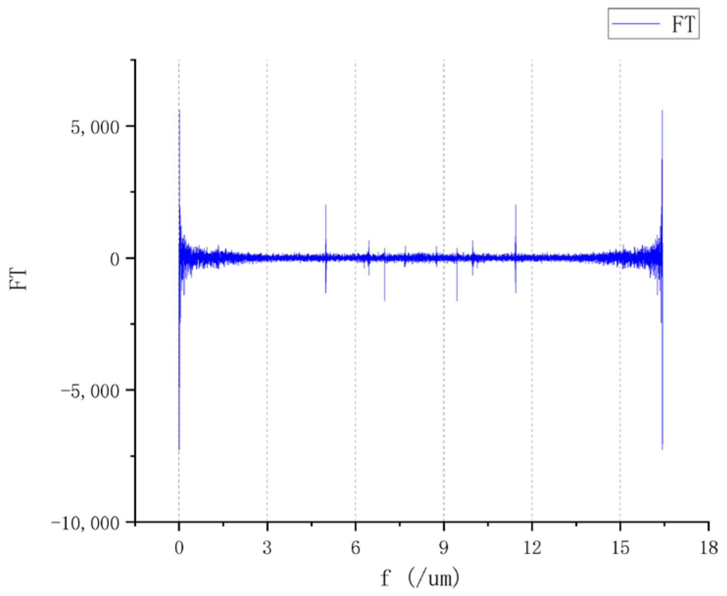
Before introducing the algorithm’s flow, we first describe the frequency domain characteristics of AFM signals, where L1–5 data (w = 0.3 μm, s = 0.2 μm) were selected for the fast FT (FFT), as shown in Figure 5.
The AFM data exhibited the following characteristics (Figure 5):
  • They exhibited significant energy concentration (peak) in the frequency domain. The instantaneous power of the signal was higher than that of the noise. Hence, hard thresholding could be used for noise reduction;
  • More energy (amplitude) was distributed at low frequencies, and the noise at low frequencies was higher than the signal energy distributed at high frequencies;
  • After dividing the multiple frequency bands, the noise energy distributed in each frequency band was relatively stable, which can be regarded as a Gaussian distribution.
Therefore, we made the following assumptions regarding the denoising method:
  • This denoising method can be applied via hard thresholding in the frequency domain owing to the high energy concentration in the frequency domain;
  • With the different proportions of energy distributed in different frequency bands, a unified threshold in the entire frequency band cannot achieve precise noise elimination. Instead, multiple thresholds should be set in different frequency bands in the denoising method;
  • The noise spectra in the frequency bands still satisfy a Gaussian distribution [27,28], whose properties can be adopted to determine the threshold for each frequency band.
Based on these noise analysis and reduction assumptions, we developed a WT-FFT denoising method to reduce the AFM data noise.

3.2. WT-FT Denoising Process

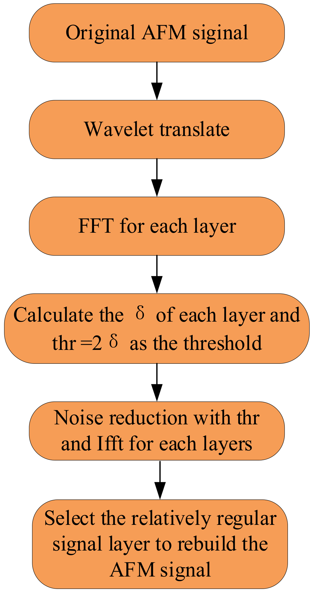
Based on the analysis of the frequency domain characteristics of the AFM signals in Section 3.1, we developed a noise reduction method using the WT-FT. The denoising process is illustrated in Figure 6. First, WT was performed on the AFM data. In the experiment, we adopted a db4 wavelet for binary wavelet decomposition to obtain the wavelet coefficients of different frequency layers. The coefficient layers were restored layer by layer to obtain the time domain components of the original signals in different frequency bands. Subsequently, FT was performed on the signal components layer by layer to obtain the frequency domain response of each component. Applying the assumptions presented in Section 3.1, we set 2σ as the noise reduction threshold by utilizing the Gaussian distribution characteristics, because the frequency domain distribution of the noise in each frequency band satisfied the Gaussian process.
After frequency domain noise reduction, inverse FT (IFT) was performed layer by layer to obtain denoising signals in each frequency band. The relatively regular signal components were analyzed and selected for signal reconstruction to obtain AFM signals without noise. Figure 7 shows the structural diagram of the entire system.

3.3. Noise Reduction Threshold Determination and Component Analysis

Two points in this process are explained, namely, threshold determination and component extraction.
(a)
Threshold determination
In the introduction of Section 3.1, the noise generated via AFM cantilever oscillation satisfies a Gaussian distribution. Mallat [11] and Labuda et al. [29] demonstrated that high-frequency random noise in AFM data are Gaussian noise. Because the FT of the Gaussian distribution probability density function also conforms to a Gaussian distribution, the frequency domain representation of the generated noise reveals the Gaussian distribution characteristics. Before performing the FT, we normalized the data such that the mean value of the noise and signal was zero. If the frequency domain noise satisfies n~N (0, σ), it can be inferred from the Gaussian distribution density function that P(abs(n) > 2 σ) < 0.05 [30]. Based on the assumptions in Section 3.1, the instantaneous power of the signal exceeded that of the noise. Therefore, in the FT F(n) of the AFM data, there is a high probability that it does not belong to a noise frequency component if F(n) exceeds 2σ. Thus, 2σ can be adopted as a hard threshold for noise filtering in the frequency domain.
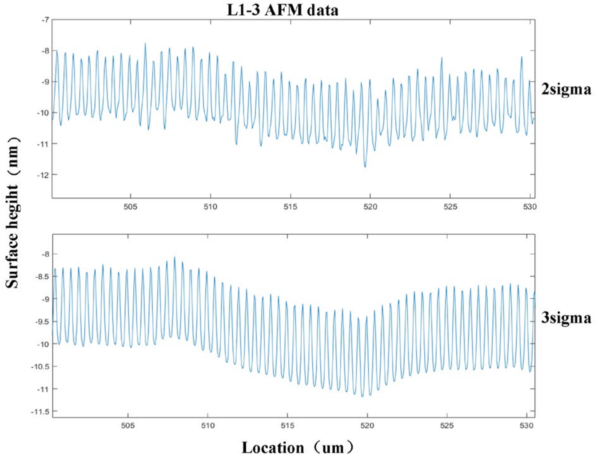
It is crucial to clarify why 3σ was disregarded as the noise threshold. According to Gaussian distribution characteristics, P(abs(n)) > 3σ < 0.005. In theory, 3σ can discard noise more precisely than 2σ as a hard threshold for noise reduction. However, our identification of these frequency domain noise characteristics was flawed. The frequency domain points in F(n) that are higher than 2σ are most likely not noise, which is not equivalent to the absence of signal frequency components when F(n) is lower than 2σ. Therefore, if the hard threshold is set to 3σ, the damage to the signal increases, while more noise is discarded. We carefully set the denoising hard threshold to 2σ to retain a specific amount of residual noise and prevent the signal loss triggered by excessive noise reduction. Figure 8 shows the local shape of the L1-3 noise reduction data obtained using 2sigma and 3sigma as the threshold, respectively. It can be seen that the shape detail data obtained by 3sigma are neat, unlike the natural data, which means that too many data burrs are removed.
(b)
Component screening
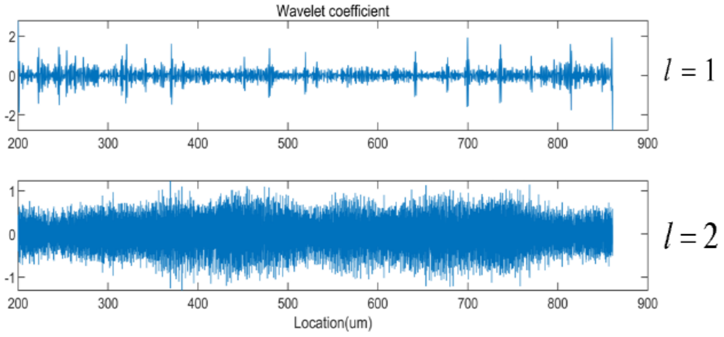
As shown in Figure 7, it is necessary to select components to reconstruct the AFM signals after denoising the different signal components. Based on the layout structure introduced in Section 1, the noise-free AFM data should present a neat and periodic outline. Because of the trench design, ideal noise-free AFM data should exhibit regularity and periodicity. For each signal component after noise reduction, the irregular and nonperiodic components introduce uncertainty to the noise-free signals when rebuilt. Therefore, we considered the nonperiodic components as the residual noise after Fourier noise reduction. After IFT, we directly observed the neatness of each frequency component from the perspective of the time domain, as shown in Figure 9. The components “ l = 1 ” distinctively belong to the noise category, which can be discarded via human observation. An advantage of multiresolution WT analysis is that the signal characteristics can be simultaneously observed in the time and frequency domains to achieve data noise reduction. This was the reason for using the WT before the FFT; we can select the effective signal component with its time domain feature.
Considering the errors in human observations and the impossibility of denoising multiple groups of signals automatically, we attempted to describe the regularity and periodicity of frequency components using information entropy [31,32,33]. This represents the amount of data contained in a signal. When the information entropy of a data piece was greater, less redundant information was observed in the signal, and the periodicity and regularity of the information were lower. The information entropy was calculated using Equation (8), where H(x), i, and P(xi) denote the information entropy of discrete data xi, a data point mark, and the probability that xi occurs at all the data points, respectively.
H ( x ) = i P ( x i ) log 2 ( P ( x i ) )
In actual computations, the effort exerted in calculating P(xi) for each data point is cumbersome owing to the large quantity of data points in the discrete AFM data. Component selection is a small part of the entire noise reduction process when short computation times are required. Hence, we divided N AFM data points xi from max(x) to min(x) into 10 intervals, counted the number of points xi in each interval (n1, n2, …n10), and calculated the probability of data points falling in each interval (Pi = ni/N|i = 1, 2, 3…10). The simplified information entropy can be calculated using Equation (9). After calculating the information entropy of each component, we evaluated the regularity of the component signal and decided whether to discard the component.
H ( x ) = i P i log 2 ( P ( x i ) )

4. Data Denoising Verification and Analysis

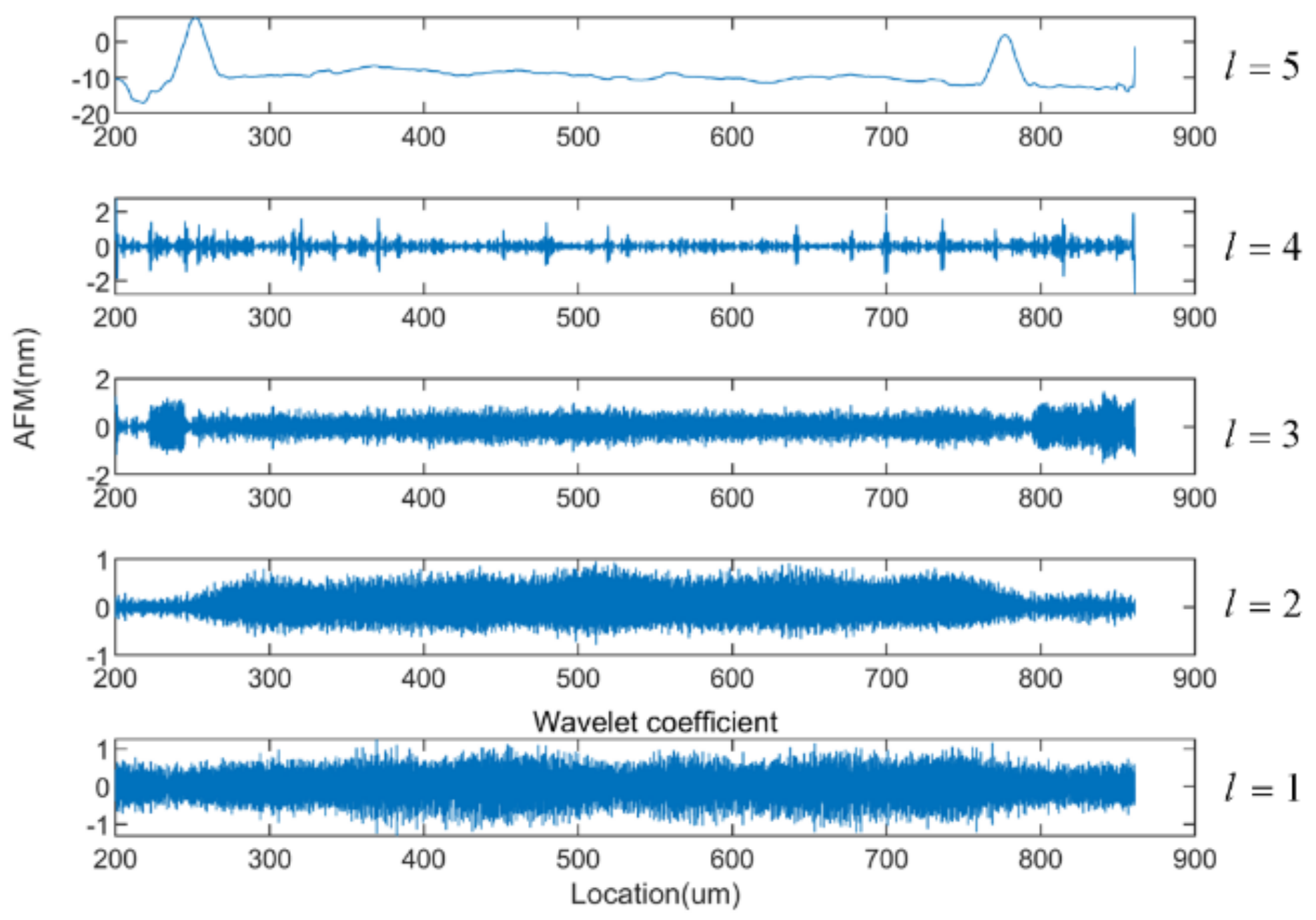
We consecutively input the AFM raw data (with noise) introduced in Section 1 into the constructed noise reduction system. Here, L1–5 (0.3 μm, 0.2 μm) is adopted as an example to verify the denoising results. The wavelet coefficients in each frequency band were obtained in binary DWT. The l = 5 layer demonstrates that the wavelet coefficient in the signal was the lowest frequency band in the original AFM data, and reveals the overall trend of the original morphology data, which can also be considered the base of the surface morphology. l = 1 4 denotes the morphology details, and the dishing information focused on CMP modeling was included in the detailed parameters. Because the base data contained detailed information about the morphology data, frequency domain filtering was not required (even if frequency domain filtering is conducted, we cannot verify whether the filtering results are accurate). In contrast, we performed simple low-frequency filtering on l = 5 layer coefficients to facilitate the data variation observation, and applied the algorithm introduced in Section 3 to perform FT and hard thresholding on the decomposed wavelet coefficients, layer by layer. The wavelet coefficients after noise reduction were obtained, as shown in Figure 10.
The advantage of the WT is that the decomposed wavelet coefficients contain both time and frequency domain information. In Figure 7, l = 1 5 represents the time domain components of the AFM data in different frequency bands. Because the actual layout design had a regular trench structure, the corresponding chip surface was supposed to have a relatively regular periodic structure. The periodicity and regularity of data components for l = 4 (Figure 10) were significantly lower than those of the other three detailed components ( l = 1 3 ); hence, we discarded the l = 4 component, excluding it from the final reconstruction of AFM data.
To reduce the manual selection errors and achieve automatic component screening while denoising multiple AFM datasets, we selected the components based on their information entropies. The specific approach was to calculate the information entropy of each component using Equation (9) in Section 3, and screen out the component that deviated the farthest from the average entropy values among the information entropies of four detailed components. Without quantitative derivation for verification, the method yielded satisfactory noise reduction results in actual filtering. The L1–5 AFM data without noise are presented in Figure 11.
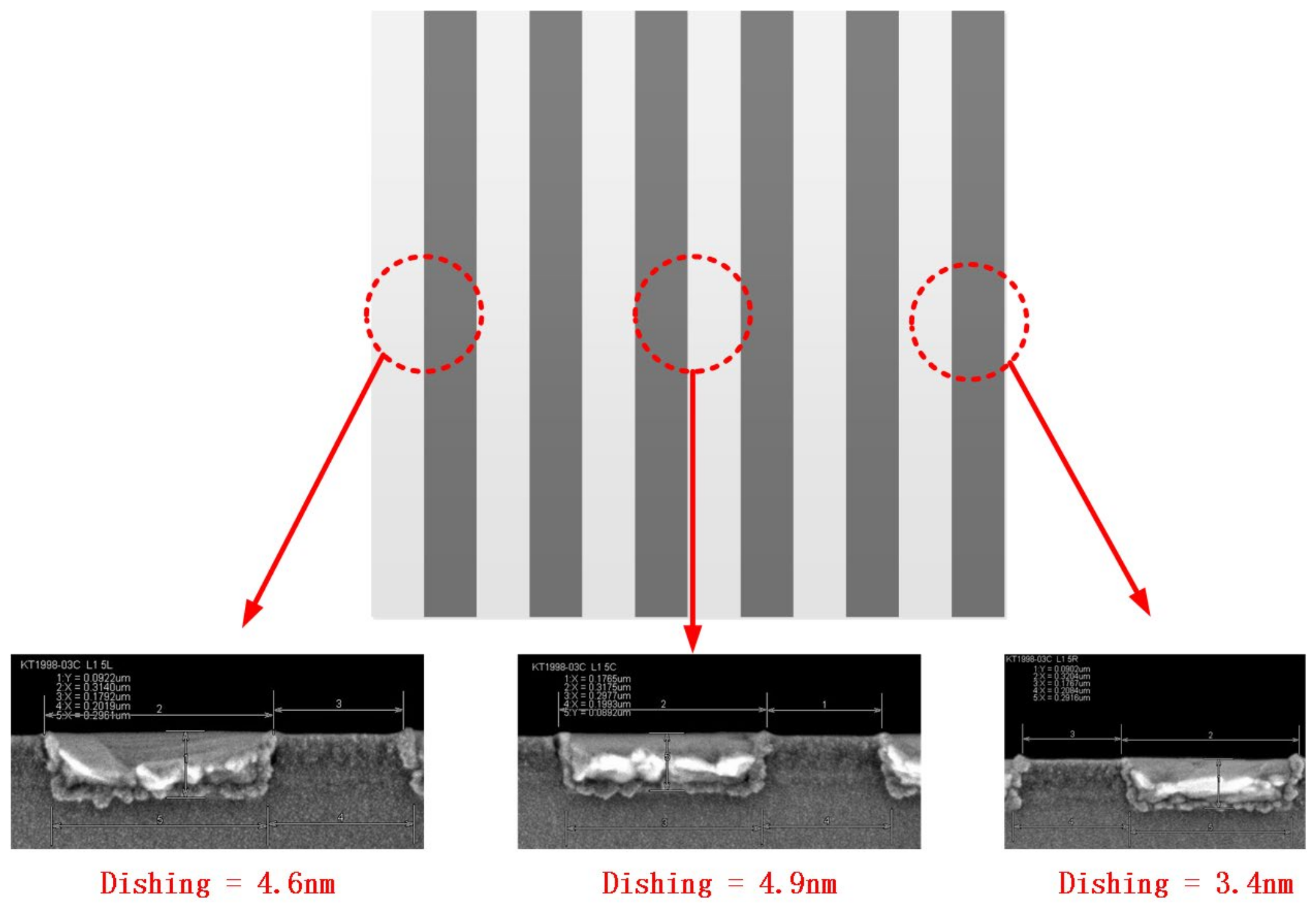
The AFM morphology data after denoising were smoothened, making it easy for researchers to measure dishing and erosion. We did not select a specific frequency band for frequency screening during noise reduction; instead, we denoised the AFM data based on the energy distribution. The frequency values of the obtained noise-free data are consistent with the graphic cycle of the layout design, indirectly verifying the favorable denoising results of the WT-FFT noise-reduction method when applied to AFM data. To further validate the effect of the denoising method, we selected some tapeout structures for SEM and obtained the cross-section data of the observed structures, including the related absolute thickness data for comparison with the noise-free AFM data. Because SEM and AFM are different methods for assessing surface morphology, the types and sources of data noise measured using both techniques are different, with SEM generally less affected by noise than AFM. Consequently, SEM cross-section data can be adopted based on the AFM data for verifying the noise reduction results. The SEM photographs of L1–5 are shown in Figure 12. We performed SEM measurements at three positions in the L1–5 structures and calculated the dishing at these positions for comparison with the AFM data.
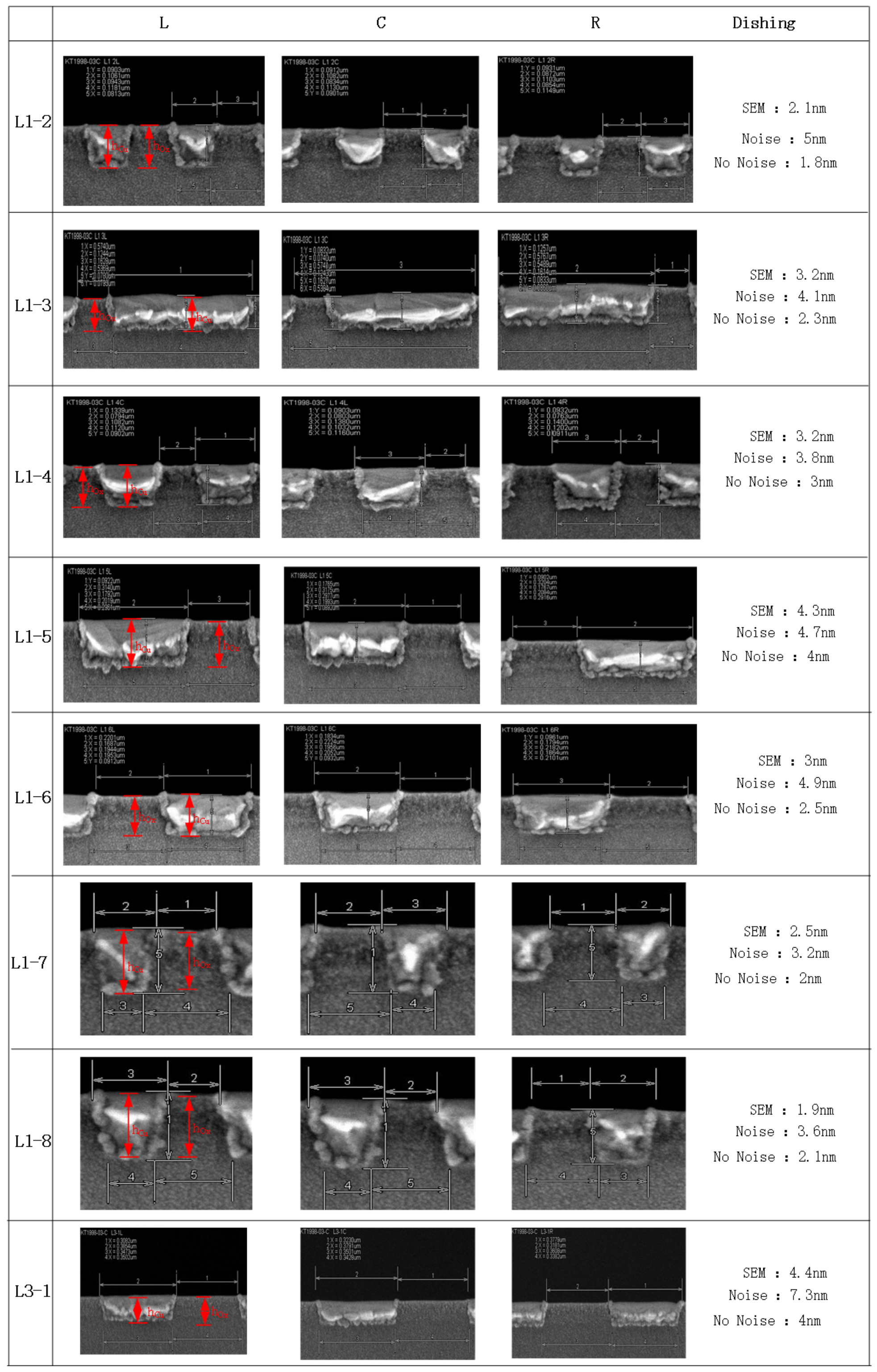
The local dishing at the three locations was calculated (dishing = TOxi − TCu) based on the absolute thickness of Cu in the SEM data, and the medium. The average dishing value at the locality and the dishing values extracted from the AFM data before and after noise reduction were compared. It was found that the denoised AFM data were closer to the actual surface morphology. All the SEM photographs are shown in Figure 13 The average dishing value extracted via SEM and the dishing values extracted from the AFM data before and after noise reduction are presented in Figure 14.
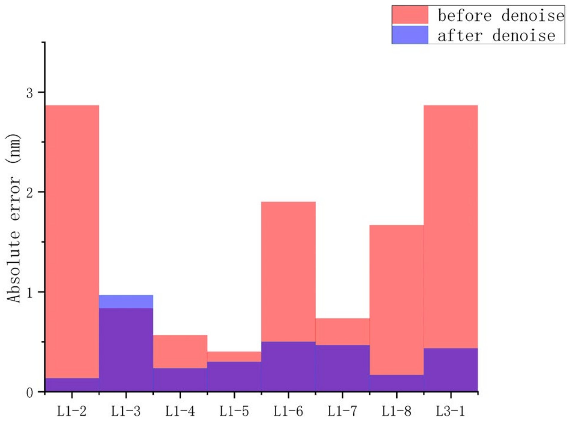
Based on a comparison between the AFM data before and after noise reduction using the SEM photographs, it was observed that the dishing values measured using the denoised AFM data were closer to the SEM data for small-sized structures (in periods less than 1 μm). To quantitatively describe the improvement in the data measurement accuracy via noise reduction, we calculated the error between the AFM data measurement dishing and the SEM data before and after noise reduction. Figure 15 shows the absolute error for a clearer contrast. The root mean square errors before and after data denoising were 4.95 and 1.33 nm, indicating that the AFM data after noise reduction were closer to the actual chip surface morphology presented by SEM.
It can be seen from Figure 14 and Figure 15 that the AFM data are more consistent with the SEM data after noise reduction. However, it can also be found that the root mean square error performance of the AFM data after noise reduction is worse than that of the SEM data in the L1_3 region of the morphological data. This set of data does not prove that the noise-reduced data are closer to the real shape. In our opinion, this phenomenon can be explained in two ways: First, the dishing measured in AFM data is the mean height difference average of a region. However, that measured from SEM data is the height difference of a local point. Therefore, there may be a high absolute error between local dishing and regional average dishing. Second, both AFM data and SEM data have observational random errors when derived via human measurement. The random observation error of L1–3 is large, so the absolute error of the data after noise reduction is similar to that before noise reduction. This is just a coincidence.
Therefore, the morphological data of the L1_3 region cannot prove the effectiveness of noise reduction. However, they equally do not prove that the noise reduction algorithm is defective. The poor performance of a single group of data may be due to the random error of the data.
In general, the WT-FT noise reduction algorithm introduced above has a good noise reduction effect when applied to AFM data reduction in the direction of CMP modeling. It can effectively reduce the measurement noise of the surface morphology of small-sized structures. It is convenient for researchers to observe the chip surface morphology after CMP. The algorithm takes advantage of the wavelet transform to retain both time domain and frequency domain information of the signal. It also combines the morphological data of CMP modeling and noise characteristics to achieve noise reduction. However, although the algorithm is effective, the overall algorithm is still relatively crude. Some parameters are still determined empirically rather than computationally. For example, the selection of the noise reduction wavelet type, the number of wavelet transform layers, and the spectral noise reduction threshold all lack scientific qualitative proof.

5. Conclusions and Outlook

The work presented in this paper focuses on solving the problem of noise reduction in AFM data measurement during CMP modeling. In this work, we show the commonly used plate structure for CMP modeling and the chip surface morphology data noise after die flow. We argue that such measurement noise is mainly caused by probe vibration and tilting during AFM measurements. In addition, we analyze the noise characteristics of such AFMs from a frequency domain perspective. It is found that the frequency domain behavior of the noise can be approximated as local Gaussian noise. Based on this feature, we have designed a noise reduction method based on WT-FT and achieved good noise reduction results. The noise reduction algorithm uses the noise threshold from the energy perspective to achieve noise reduction. The processing of the original AFM data by wavelet decomposition and FT causes the data information to be decomposed into multiple frequency domain components. This decomposition method yields high accuracy for hard-threshold noise reduction in the frequency domain, allowing for maximum noise rejection while preserving morphological data. Indirect qualitative proof is given in that the morphological period after noise reduction is consistent with the structural period of the layout design. The data frequencies were not screened during the noise reduction process; however, the noise reduction data cycles were similar to the target cycles, demonstrating the feasibility of the noise reduction method.
In addition, the comparison of the results with morphological data obtained from SEM photographs verifies that the noise-reduced data were closer to the actual morphology, quantitatively validating the noise reduction method. Although there are individual data with high errors, the phenomenon is considered to be due to random errors. This does not affect the proof of the effectiveness of the noise reduction algorithm. At the same time, the method exhibits a high degree of scalability because the user can adjust the noise reduction results by fine-tuning the number of WT decomposition layers, wavelet basis functions and frequency domains.
We propose to use information entropy comparison to filter the time domain components after noise reduction. However, this approach is relatively complicated for such problems due to the lack of mathematical support and some unsatisfactory screening results. We expect to develop more effective screening and denoising validation methods in the future, and to incorporate the characteristics of the measured data. Meanwhile, the noise reduction algorithm is relatively crude in design, and there are many ways in which it can be proven, as well as improved—for example, the quantitative proof of the noise reduction threshold, the selection of wavelet function and the determination of the optimal number of wavelet decomposition layers. At present, such parameters are still determined empirically and require several attempts. We hope to improve the noise reduction algorithm in all aspects in future work to make it more operable and achieve a better noise reduction performance.

Author Contributions

Conceptualization, B.R.; methodology, B.R. and L.C.; software, B.R.; validation, B.R., R.C. and Y.W., formal analysis, B.R. and R.J.; investigation, B.R. and R.J. All authors have read and agreed to the published version of the manuscript.

Funding

This work was supported in part by the Foundation for Research on intelligent EDA tool for CMP process simulation of IC wafer manufacturing based on the “Big Data + Artificial Intelligence” paradigm, under Grant CAS-WX2021SF-0113.

Data Availability Statement

Data are partly contained within the article. Due to confidentiality, raw data cannot be disclosed.

Conflicts of Interest

The authors have no conflict of interest to declare.

Correction Statement

This article has been republished with a minor correction to the existing affiliation information. This change does not affect the scientific content of the article.

References

  1. Xie, X. Physical Understanding and Modeling of Chemical Mechanical Planarization in Dielectric Materials. Ph.D. Thesis, Massachusetts Institute of Technology, Cambridge, MA, USA, 2007. [Google Scholar]
  2. Park, T.H. Characterization and Modeling of Pattern Dependencies in Copper Interconnects for Integrated Circuits. Ph.D. Thesis, Massachusetts Institute of Technology, Cambridge, MA, USA, 2002. [Google Scholar]
  3. Tugbawa, T.E.; Park, T.H.; Boning, D.S. Integrated chip-scale simulation of pattern dependencies in copper electroplating and copper chemical mechanical polishing processes. In Proceedings of the IEEE 2002 International Interconnect Technology Conference (Cat. No.02EX519), Burlingame, CA, USA, 5 June 2002. [Google Scholar] [CrossRef][Green Version]
  4. Geng, C.; Liu, B.; Nakatake, S. Density Optimization for Analog Layout Based on Transistor-Array. IEICE Trans. Fundam. Electron. Commun. Comput. Sci. 2019, E102, 1720–1730. [Google Scholar] [CrossRef]
  5. Ghulghazaryan, R.; Wilson, J.; Abouzeid, A. FEOL CMP modeling: Progress and challenges. In Proceedings of the 2015 International Conference on Planarization/CMP Technology, Chandler, AZ, USA, 30 September–2 October 2015; pp. 1–4. [Google Scholar]
  6. Tugbawa, T.; Park, T.; Boning, D.; Pan, T.; Li, P.; Hymes, S.; Brown, T.; Camilletti, L. A mathematical model of pattern dependencies in Cu CMP processes. In Proceedings of the CMP Symposium, Electrochemical Society Meeting, Honolulu, HA, USA, 17–22 October 1999; pp. 605–615. [Google Scholar]
  7. Francisco, L.; Mao, R.; Katakamsetty, U.; Verma, P.; Pack, R.C. Multilayer CMP hotspot modeling through deep learning. In Design-Process-Technology Co-Optimization Manufacturability XIII; SPIE: Bellingham, WA, USA, 2019; Volume 10962, pp. 202–213. [Google Scholar] [CrossRef]
  8. Tripathi, S.; Monvoisin, A.; Dornfeld, D.; Doyle, F.M. CMP Modeling as a part of Design for Manufacturing. In Proceedings of the International Conference on Planarization/CMP Technology, Dresden, Germany, 25–27 October 2007; pp. 1–6. [Google Scholar]
  9. Liew, S.W.; Leong, L.S.; Whsu, R.; Chong, Y.S. Poly CMP Process Challenges for Embedded Array Devices. In Proceedings of the 2021 32nd Annual SEMI Advanced Semiconductor Manufacturing Conference (ASMC), Milpitas, CA, USA, 10–12 May 2021; pp. 1–5. [Google Scholar] [CrossRef]
  10. Ruan, W.; Chen, L.; Ma, T.; Fang, J.; Zhang, H.; Ye, T. Optimization of a Cu CMP process modeling parameters of nanometer integrated circuits. J. Semicond. 2012, 33, 086001. [Google Scholar] [CrossRef]
  11. Tanwar, K.; Canaperi, D.; Lofaro, M.; Tseng, W.-T.; Patlolla, R.; Penny, C.; Waskiewicz, C. BEOL Cu CMP process evaluation for advanced technology nodes. J. Electrochem. Soc. 2013, 160, D3247. [Google Scholar] [CrossRef]
  12. Toffoli, A.; Maitrejean, S.; De Pontcharra, J.D.; De Crécy, F.; Bouchu, D.; Arnaud, L.; Boulanger, F. Test structure for characterizing metal thickness in damascene CMP technology. In Proceedings of the 2008 IEEE International Conference on Microelectronic Test Structures, Edinburgh, UK, 24–27 March 2008; pp. 210–213. [Google Scholar] [CrossRef]
  13. Gomez, C.; Su, R.; de Groot, P.; Leach, R. Noise Reduction in Coherence Scanning Interferometry for Surface Topography Measurement. Nanomanuf. Metrol. 2020, 3, 68–76. [Google Scholar] [CrossRef][Green Version]
  14. Jones, L.; Yang, H.; Pennycook, T.J.; Marshall, M.S.J.; Van Aert, S.; Browning, N.D.; Castell, M.R.; Nellist, P.D. Smart align-A new tool for robust non-rigid registration of scanning microscope data. Adv. Struct. Chem. Imaging 2015, 1, 8. [Google Scholar] [CrossRef]
  15. Lapshin, R.V. Automatic drift elimination in probe microscope images based on techniques of counter-scanning and topography feature recognition. Meas. Sci. Technol. 2007, 907, 907–927. [Google Scholar] [CrossRef][Green Version]
  16. Dukic, M.; Adams, J.D.; Fantner, G.E. Piezoresistive AFM cantilevers surpassing standard optical beam deflection in low noise topography imaging. Sci. Rep. 2015, 5, 16393. [Google Scholar] [CrossRef] [PubMed][Green Version]
  17. Zhan, H.; Tan, X.; Xie, G.; Guo, D. Load-dependent energy dissipation induced by the tip–membrane friction on suspended 2D materials. Phys. Chem. Chem. Phys. 2021, 23, 19819–19826. [Google Scholar] [CrossRef] [PubMed]
  18. Yi, S.; Li, T.; Zou, Q. Active control of acoustics-caused nano-vibration in atomic force microscope imaging. Ultramicroscopy 2018, 195, 101–110. [Google Scholar] [CrossRef] [PubMed]
  19. Wu, Y.; Fang, Y.; Fan, Z.; Wang, C.; Liu, C. An automated vertical drift correction algorithm for AFM images based on morphology prediction. Micron 2021, 140, 102950. [Google Scholar] [CrossRef] [PubMed]
  20. Tsimbinos, J.; Lever, K.V. Input Nyquist sampling suffices to identify and compensate nonlinear systems. IEEE Trans. Signal Process. 1998, 46, 2833–2837. [Google Scholar] [CrossRef] [PubMed]
  21. Hara, T. Openloop Gain Criteria of Sampled-data Control Systems with Mechanical Resonant modes above the Nyquist Frequency. In Proceedings of the 2006 SICE-ICASE International Joint Conference, Busan, Republic of Korea, 18–21 October 2006; pp. 2771–2776. [Google Scholar] [CrossRef]
  22. Münch, B.; Trtik, P.; Marone, F.; Stampanoni, M. Stripe and ring artifact removal with combined wavelet—Fourier filtering. Opt. Express 2009, 17, 8567–8591. [Google Scholar] [CrossRef] [PubMed][Green Version]
  23. Sifuzzaman, M.; Islam, M.R.; Ali, M.Z. Application of wavelet transform and its advantages compared to Fourier transform. J. Phys. Sci. 2009, 13, 121–134. [Google Scholar]
  24. Mallat, S.G. A theory for multiresolution signal decomposition: The wavelet representation. IEEE Trans. Pattern Anal. Mach. Intell. 1989, 11, 674–693. [Google Scholar] [CrossRef][Green Version]
  25. Mallat, S. A Wavelet Tour of Signal Processing; Elsevier: Amsterdam, The Netherlands, 1999. [Google Scholar]
  26. Shi, J.; Liu, X.; Zhang, N. On uncertainty principle for signal concentrations with fractional Fourier transform. Signal Process. 2012, 92, 2830–2836. [Google Scholar] [CrossRef]
  27. Labuda, A.; Lysy, M.; Paul, W.; Miyahara, Y.; Grütter, P.; Bennewitz, R.; Sutton, M. Stochastic noise in atomic force microscopy. Phys. Rev. E 2012, 86, 031104. [Google Scholar] [CrossRef] [PubMed][Green Version]
  28. Labuda, A.; Lysy, M.; Gruetter, P. Stochastic simulation of tip-sample interactions in atomic force microscopy. Appl. Phys. Lett. 2012, 1, 053121. [Google Scholar] [CrossRef][Green Version]
  29. Jain, A.; Gupta, R. Gaussian filter threshold modulation for filtering flat and texture area of an image. In Proceedings of the 2015 International Conference on Advances in Computer Engineering and Applications, Ghaziabad, India, 19–20 March 2015; pp. 760–763. [Google Scholar]
  30. Starck, J.-L.; Murtagh, F.; Gastaud, R. A new entropy measure based on the wavelet transform and noise modeling [image compression]. IEEE Trans. Circuits Syst. II Analog. Digit. Signal Process. 1998, 45, 1118–1124. [Google Scholar] [CrossRef]
  31. Hughes, M.S. Analysis of ultrasonic waveforms using Shannon entropy. In Proceedings of the IEEE 1992 Ultrasonics Symposium Proceedings, Tucson, AZ, USA, 20–23 October 1992; Volume 2, pp. 1205–1209. [Google Scholar] [CrossRef]
  32. Hughes, M.S. Analysis of digitized waveforms using Shannon entropy. J. Acoust. Soc. Am. 1993, 93, 892–906. [Google Scholar] [CrossRef]
  33. Hughes, M.S. Analysis of digitized waveforms using Shannon entropy. II. High-speed algorithms based on Green’s functions. J. Acoust. Soc. Am. 1994, 95, 2582–2588. [Google Scholar] [CrossRef]
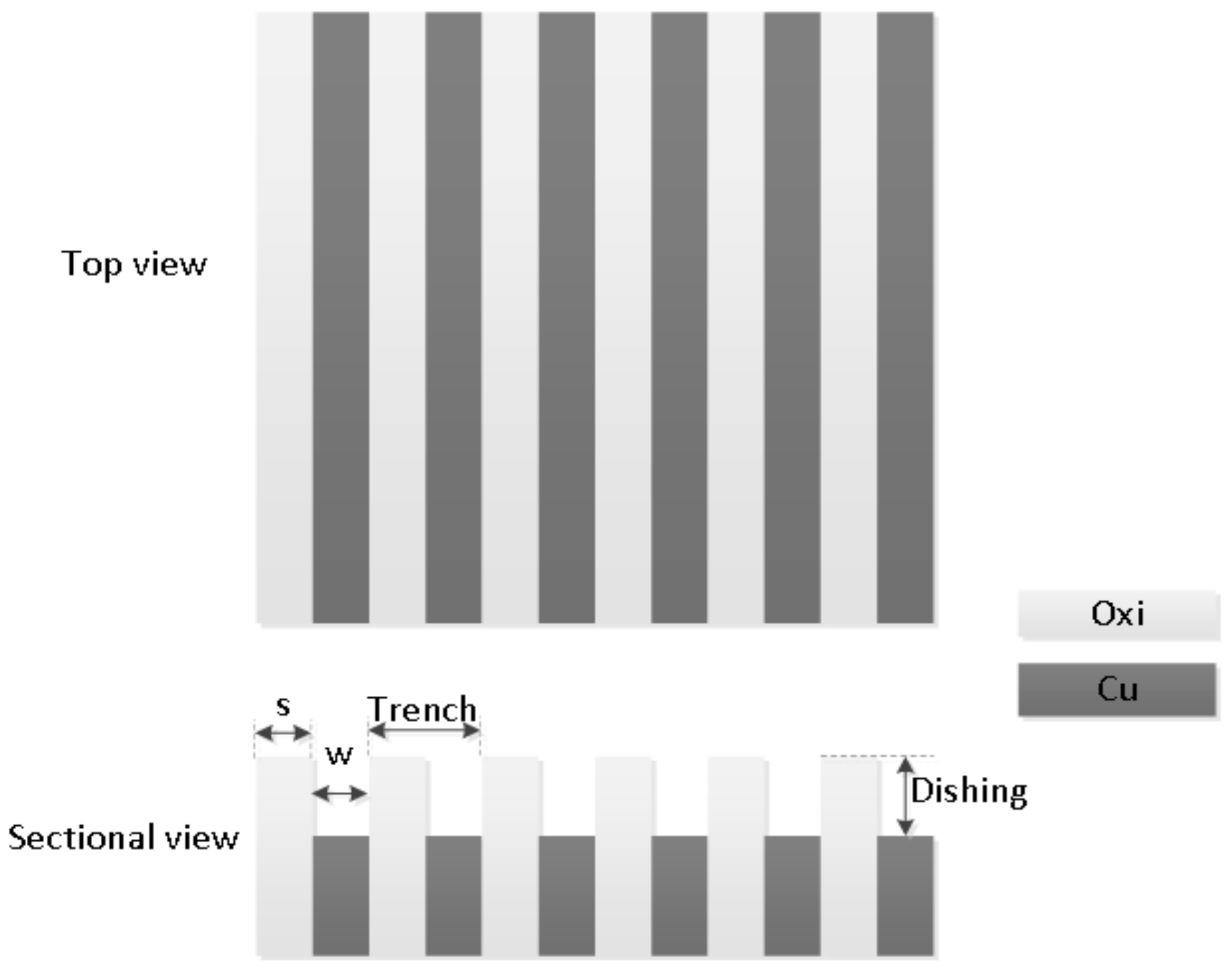
Figure 1. Trench structure of layout design.
Electronics 12 02422 g001
Figure 2. L1–L3 represent the schematic of layout design. The layout structure is a 500 μm square trench array with 18 across three rows.
Electronics 12 02422 g002
Figure 3. L1_5 array AFM topography data and local details. The local details show the glitch noise, and the skew of data shows the slope noise.
Electronics 12 02422 g003
Figure 4. Schematic of Mallat fast algorithm for WT. W 0 , 0 is the original discrete signal. l is the decomposition level in Equation (7). W j , 0 is equal to c L , n , and W j , 1 is equal to d l , n in Equation (7). H(f) and G(f) are the low- and high-pass filters, respectively, shown in the Mallat fast algorithm.
Electronics 12 02422 g004
Figure 5. Spectrum distribution of AFM data (L1–5) with noise.
Electronics 12 02422 g005
Figure 6. Flow chart of WT-FT noise reduction algorithm.
Electronics 12 02422 g006
Figure 7. Diagram of WT-FFT noise reduction method structure.
Electronics 12 02422 g007
Figure 8. L1–3 shape noise reduction data (local).
Electronics 12 02422 g008
Figure 9. Wavelet coefficients of each frequency band after noise reduction. Compared with l = 2 , the component l = 1 is worse in terms of periodicity. Therefore, we considered l = 1 a noise component and eliminated it.
Electronics 12 02422 g009
Figure 10. Wavelet coefficients of each frequency band after noise reduction of L1–5 topography data.
Electronics 12 02422 g010
Figure 11. L1–5 morphology AFM data after denoising. From local amplification, data after denoising became smooth and neat.
Electronics 12 02422 g011
Figure 12. SEM sampling section position and images.
Electronics 12 02422 g012
Figure 13. SEM images and dishing calculation, where dishing = hCu−hox.
Electronics 12 02422 g013
Figure 14. Dishing of arrays calculated from SEM images, AFM data, and AFM data after denoising.
Electronics 12 02422 g014
Figure 15. Absolute error calculated in comparison with AFM before and after denoising with SEM data. The dishing measured from AFM data after denoised are closer to the SEM results than those measured from the original AFM.
Electronics 12 02422 g015
Table 1. Parameter of trench array.
ArrayLine Width
(μm)
Line Space
(μm)
Pitch
(μm)
Density
L1_11.0001.0002.0000.500
L1_20.1000.1000.2000.500
L1_30.5600.1400.7000.800
L1_40.1500.0650.2150.698
L1_50.3000.2000.5000.600
L1_60.2000.2000.4000.500
L1_70.0450.0900.1350.333
L1_80.0750.0750.1500.500
L2_12.0003.0005.0000.400
L2_24.0001.0005.0000.800
L2_34.0002.0006.0000.667
L2_43.0009.00012.0000.250
L2_54.5004.5009.0000.500
L2_61.1200.2801.4000.800
L2_70.1000.4000.5000.200
L2_80.0450.0450.0900.500
L3_10.3500.3500.7000.500
L3_20.5000.5001.0000.500
L3_30.8000.8001.6000.500
L3_42.0002.0004.0000.500
L3_54.5001.0005.5000.818
L3_62.0001.3003.3000.606
L3_70.7000.3001.0000.700
L3_81.0004.0005.0000.200
Disclaimer/Publisher’s Note: The statements, opinions and data contained in all publications are solely those of the individual author(s) and contributor(s) and not of MDPI and/or the editor(s). MDPI and/or the editor(s) disclaim responsibility for any injury to people or property resulting from any ideas, methods, instructions or products referred to in the content.