Communication

A Q-Band CMOS Image-Rejection Receiver Integrated with LO and Frequency Dividers

School of Electrical Engineering, Korea University, Anam-dong, Seongbuk-gu, Seoul 02841, Republic of Korea
*
Author to whom correspondence should be addressed.
Electronics 2023, 12(14), 3069; https://doi.org/10.3390/electronics12143069
Submission received: 12 May 2023 / Revised: 22 June 2023 / Accepted: 10 July 2023 / Published: 13 July 2023
(This article belongs to the Special Issue Recent Advances in RF and Millimeter-Wave Design Techniques)

Abstract

:
This paper presents a Q-band image-rejection receiver using a 65 nm CMOS technology. For a high image-rejection ratio (IMRR), the Q-band receiver employs the Hartley architecture which consists of a Q-band low-noise amplifier, two down-conversion mixers, a 90° hybrid coupler, and two IF baluns. In addition, a Q-band fundamental voltage-controlled oscillator (VCO) and a frequency divider chain divided by 256 are integrated into the receiver for LO. A charge injection technique is employed in the mixers to reduce the DC power while maintaining a high conversion gain and linearity. The VCO adopts a cross-coupled topology to secure stable oscillation with high output power in the Q-band. The frequency divider chain is composed of an injection-locked frequency divider (ILFD) and a multi-stage current-mode logic (CML) divider to achieve a high division ratio of 256, which facilitates the LO signal locking to an external phase-locked loop. An inductive peaking is employed in the ILFD to widen the locking range. The Q-band image-rejection receiver exhibits a peak conversion gain of 16.4 dB at 43 GHz. The IMRR is no less than 35.6 dBc at the IF frequencies from 1.5 to 5 GHz.

1. Introduction

The development of mobile devices and the need for high-speed communication have resulted in considerable research on receivers operating in the mm-wave frequency bands [1,2,3,4,5,6,7,8,9,10,11,12,13,14,15,16,17]. In [2,3,4], the beamforming receivers were implemented by combining four channels [2,3] and eight channels [4], respectively. In [5,6], direct-conversion receivers were presented for low power consumption and small chip area. Although the direct conversion was free from the image problem, the architecture suffered from high DC offset, even-order distortion, and flicker noise [18]. In [13], a high image-rejection ratio (IMRR) over a wide bandwidth was obtained using a single-sideband receiver structure with a high IF. However, such a high IF frequency would require additional down-conversion to the baseband, and the first down-conversion mixer may suffer from compression or self-mixing due to the LO frequency interference. In [14,15], a high IMRR was achieved in the low-IF band by using a Hartley-structured receiver with a quadrature generator that minimized the I-Q mismatch. However, these studies did not include an LO circuit integrated in the receiver, so additional VCO and frequency dividers were required for phase-locked LO generation.
This paper presents a Q-band image-rejection receiver employing the Hartley architecture for a high IMRR [19]. Furthermore, the receiver integrates an on-chip voltage-controlled oscillator (VCO) and frequency divider chain for LO generation. The divider chain is composed of an injection-locked frequency divider (ILFD) and a seven-stage current-mode logic (CML) divider, which fulfill a high division ratio of 256. This facilitates the LO locking to an external phase-locked loop (PLL). This Q-band image-rejection receiver was implemented using a 65 nm bulk CMOS technology, which is relatively cost-effective and easily accessible. The remainder of the paper is organized as follows. In Section 2, the architecture of the Q-band image-rejection receiver is described. The design and measurement of each circuit block of the receiver is presented in Section 3. Section 4 presents the measurement of the Q-band image-rejection receiver. Finally, the conclusions are presented in Section 5.

2. Q-Band Image-Rejection Receiver Architecture

Figure 1 shows the block diagram of the Q-band image-rejection receiver. The image-rejection receiver is composed of a Q-band low-noise amplifier (LNA), two down-conversion mixers, a 90° hybrid coupler, two IF baluns, a Q-band VCO, and a frequency divider chain. The receiver adopts the Hartley image-rejection architecture for a high IMRR. The RF input is amplified and divided with a phase difference of 180 degrees through the single-to-differential Q-band LNA and applied to the two Q-band down mixers. The LO signal generated by the Q-band VCO is divided with a phase difference of 90° through the 90° hybrid coupler and drives two down-conversion mixers, respectively. The differential IF outputs generated by each mixer are added in-phase at the output of the IF balun, and combined through the off-chip IF 90° hybrid coupler. The desired IF signal down-converted through the two down-conversion mixers is added in-phase, and the image signal is canceled out by out-of-phase.
The Q-band VCO operates in the fundamental mode to suppress the spurious spectral components compared to the harmonic-mode VCOs. The following frequency divider chain provides a low-frequency LO signal divided by 256. Thus, the LO signal can be readily locked to an off-chip PLL circuitry.

3. Circuit Blocks of the Q-Band Image-Rejection Receiver

In this section, the design details and measurement results of each individual circuit block of the Q-band image-rejection receiver are described.

3.1. Q-Band LNA

A schematic of the Q-band LNA is depicted in Figure 2a. The first stage of the LNA employs a single-ended structure to eliminate the noise figure (NF) component which would be otherwise contributed by an input balun. The NF is further improved by the source degeneration of a transmission line (TL1). The input is matched to the optimum NF point through L-section matching, which is composed of parallel and series inductors (L1 and L2). All transmission lines are designed in a microstrip structure using the top metal with a 1.2 μm thickness to minimize the loss and chip area, as shown in Figure 3a. The layout of the inductor and transformer are shown in Figure 3b,c, respectively. The inductors were designed in an octagonal shape using the top metal and the inductance was extracted through EM simulation. The transformers were designed using a broadside coupling structure composed of the top two metals (LB and OI).
The second to last stages were designed using a differential common-source structure with the capacitive neutralization technique to improve gain and stability. The interstage matching between the first and second stages was implemented using transmission lines (TL2–TL4) and a transformer-based balun (TF1) connected to a balancing capacitor (C1). The other interstage and output matching networks are also composed of transmission lines and transformers to reduce the chip area. The output impedance is conjugately matched to the RF input of the following Q-band down-conversion mixer. A chip micrograph of the Q-band LNA is shown in Figure 2b. The chip area is 1.7 × 0.6 mm2, which includes the probing pads. The differential output is combined into a single-ended signal using a balun (TF4) for single-ended measurement purposes. The LNA chip consumes DC power of 30 mW at the drain bias voltage of 1.2 V. The parameter value of each component is presented in Table 1.
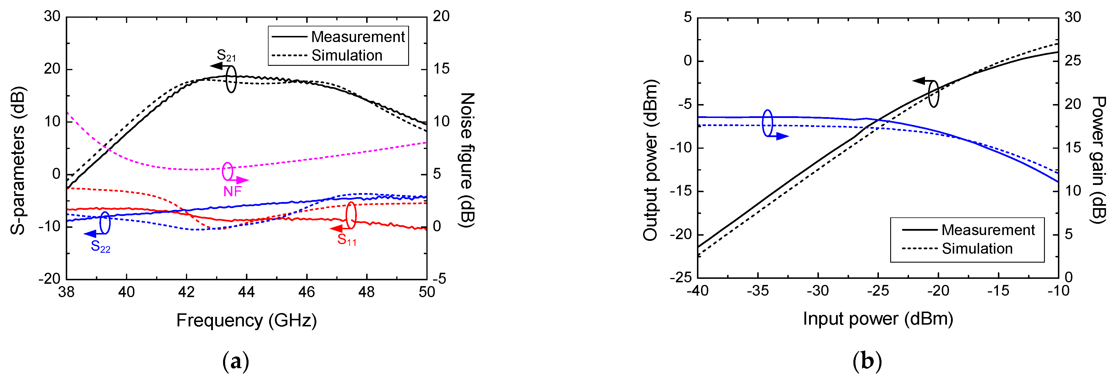
The measurement results for the Q-band LNA are shown in Figure 4. The measurement was performed by an on-chip probing method. Figure 4a shows the S-parameters and NF. A peak gain of 18.8 dB was measured at 43.3 GHz with a 3 dB bandwidth of 5.6 GHz (41.7–47.3 GHz). The input matching was measured below 7.2 dB over the entire 3 dB bandwidth while the simulated NF was below 6.9 dB. Figure 4b presents the power measurement of the LNA at 43.5 GHz. The measured input and output 1 dB compression power (IP1dB and OP1dB) were −22 dBm and −4.5 dBm, respectively.

3.2. Q-Band Down-Conversion Mixer

The Q-band down-conversion mixer was designed using a Gilbert-cell topology for a high conversion gain and isolation performance [20,21]. A schematic of the mixer is shown in Figure 5a. The charge injection through R1 and R2 is adopted at the transconductance stages to reduce DC power consumption while maintaining a high conversion gain. The RF and LO matching networks are composed of transformer-based baluns (TF5 and TF6) and series transmission lines (TL15–TL18) for broadband impedance matching and chip area reduction. Series inductors (Ls) are inserted between the transconductance and switching-quad stages to extend the RF bandwidth. A source-follower buffer was added at the output to improve the isolation and IF matching performance. The transistor sizes of the transconductance, switching-quad, and source-follower stages were 2 × 20 μm (M8 and M9), 2 × 12 μm (M10–M13), and 2 × 30 μm (M14 and M15), respectively. A chip micrograph of the Q-band down-conversion mixer is shown in Figure 5b, occupying a chip area of 1 × 0.8 mm2 including the probing pads. For a single-ended testing purpose, one of the differential output is terminated by a 50-ohm resistor. The Q-band down-conversion mixer consumes DC power of 4.57 mW at the mixer core and 3.89 mW at the source-follower buffer. The parameter value of each component is presented in Table 2.
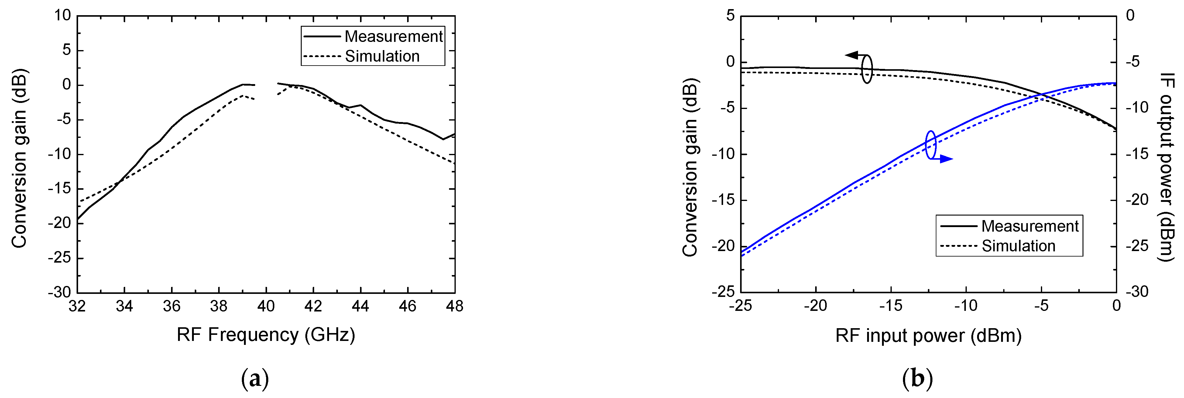
Figure 6 presents the measurement result of the Q-band down-conversion mixer. Figure 6a shows the measured conversion gain versus RF frequency with the LO power of 0 dBm applied at 40 GHz. The conversion gain exhibited a peak value of 0.25 dB at 40.5 GHz and the 3 dB bandwidth was 6.8 GHz (37.3–43.3 GHz). The conversion gain and IF output power at 1.0 GHz versus RF input power at 41.0 GHz are plotted in Figure 6b. The IP1dB of the mixer was measured to be −6.5 dBm. Since the OP1dB of the LNA was −4.5 dBm, as given in Section 3.1, the input drive power to the mixer would be −7.5 dBm taking into account a 3 dB difference due to the output balun of the LNA (TF4 in Figure 2a). Therefore, no gain compression was expected from the mixer.

3.3. Q-Band Voltage-Controlled Oscillator

Generally, there are three oscillator topologies used in the mm-wave frequency band: ring topology [22,23], Colpitts topology [24], and cross-coupled topology [25]. In this work, the cross-coupled topology was adopted as shown in Figure 7a because it provides a sufficient negative resistance, differential operation, and high output power [25]. The total gate width was set to 1.5 × 12 μm considering the trade-off between DC power consumption and output power. The LC tank was implemented using transmission lines (TL19 and TL20) and MOS varactors (Cvar). The dimensions were optimized to resonate with the input capacitance of the cross-coupled pair and the buffer transistors (M18 and M19) at 40 GHz. The Cvar tuned the capacitance from 51.6 to 146 fF with a Q-factor ranging from 4 to 7.6 at 40 GHz. The oscillation core was followed by two cascaded buffer amplifiers. The first buffer is a source follower that improves isolation and stability. Subsequently, a common-source amplifier (M20 and M21) was followed to boost the output power to the level required for pumping the Q-band down-conversion mixer. A chip micrograph of the Q-band VCO is shown in Figure 7b. For a single-ended testing purpose, the differential output was combined using the output balun (TF7). The Q-band VCO occupied a chip area of 0.7 × 0.8 mm2 including the probing pads. The DC power consumption levels of the oscillation core and buffer stage were 21.1 mW and 31.7 mW, respectively. The parameter value of each component is presented in Table 3.
In Figure 8, the measured oscillation frequency and output power of the Q-band VCO are compared with the simulation. As the varactor control voltage (VC) varied from 0 to 2.4 V, the oscillation frequency was tuned from 35.6 to 45.6 GHz (24.6%). The measured output power ranged from −2.7 to 0.6 dBm, including 2 dB of balun loss, which was added only for a measurement purpose.

3.4. Frequency Divider Chain

Three different topologies are widely used for a frequency divider at the mm-wave frequency: the injection-locked frequency divider (ILFD), Miller divider, and current-mode logic (CML) divider. Generally, the ILFD operates at the highest frequency with a low DC power consumption at the expense of a narrow bandwidth. On the other hand, the CML divider cannot support a high-frequency operation and consumes high DC power. However, it occupies the smallest chip area, particularly at relatively low frequencies [26,27]. Therefore, in this work, the frequency divider chain adopted a ILFD for the first frequency division in the Q-band, which was followed by seven CML dividers.
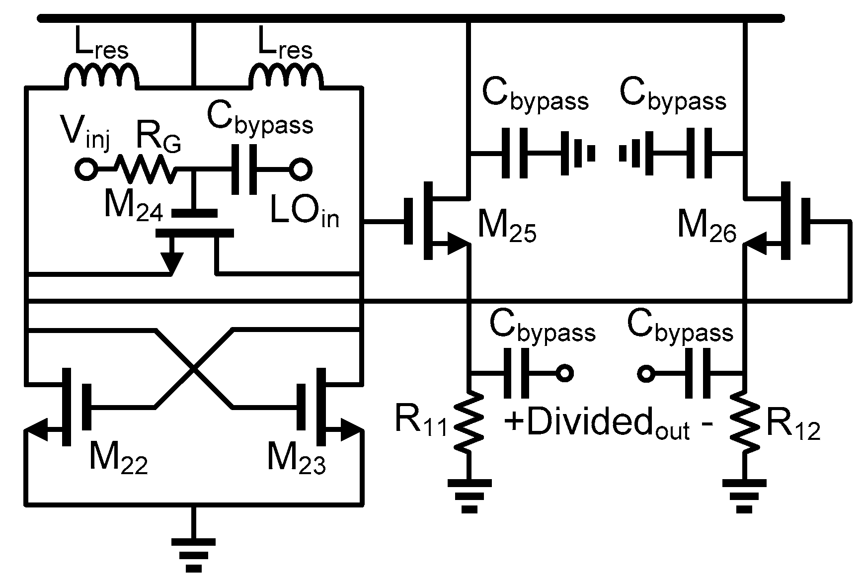
Figure 9 shows a schematic diagram of a basic Q-band ILFD, which consists of a cross-coupled oscillation core (M22 and M23), a resonator, an injection network (M24), and a source-follower buffer (M25 and M26). The resonator, composed of an inductor (Lres) and parasitic capacitances of M22–23, M24, and M25–26, resonates at f0, a half frequency of the injection signal (LOin). The LOin is injected directly into the differential oscillation core through M24. This direct injection enables the extension of the locking range (LR) at a higher operating frequency compared to conventional injection through a tail current source [28]. The LR of the direct ILFD can be expressed as [29]
L R 2 π f 0 I i n Q I o s c
where Iin and Iosc denote the injection current by LOin and oscillation current, respectively, flowing through Minj, and Rds denotes the drain-to-source resistance of Minj. Q is defined as follows:
Q R d s 2 π f 0 L r e s
According to Equation (1), the LR can be widened by increasing the injection current Iin.
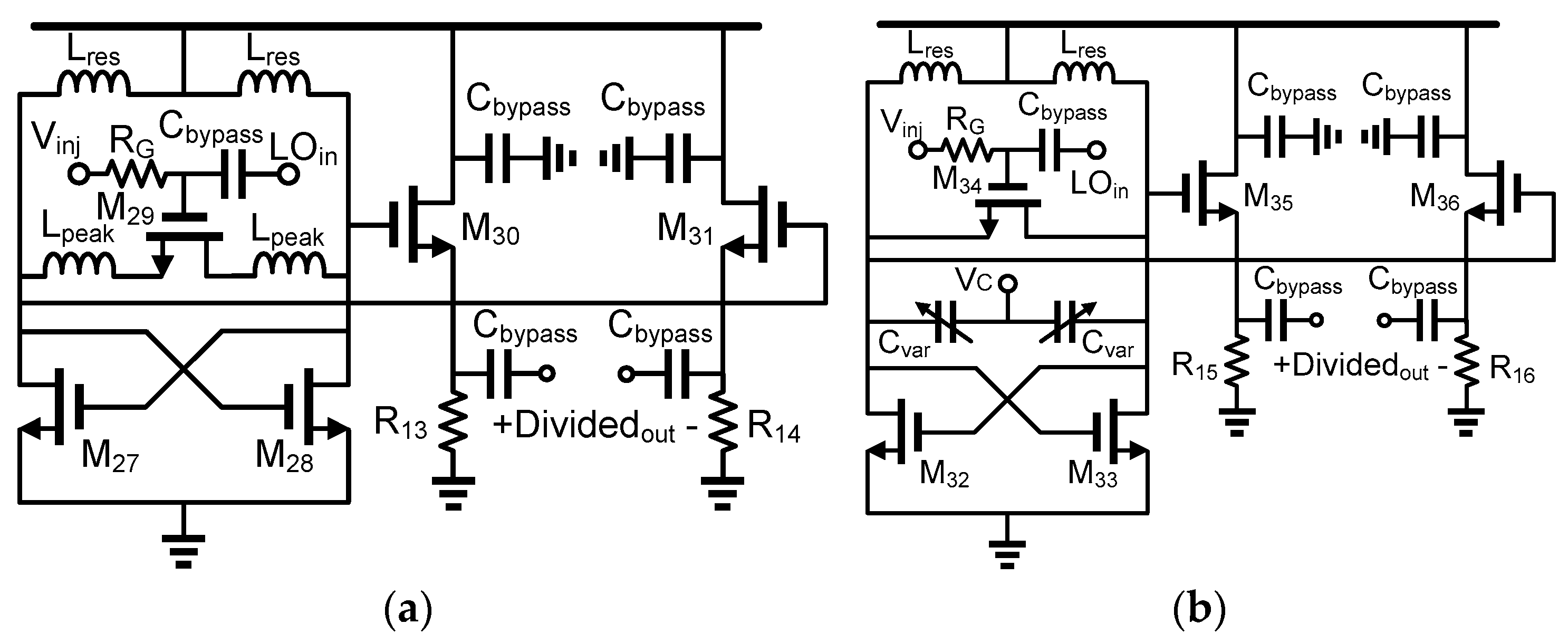
To improve LR of the basic ILFD shown in Figure 9, two variations of ILFD employing a peaking inductor and a varactor, respectively, are presented. In Figure 10a, a peaking inductor (Lpeak) is connected in series with M29j, so that the swing of Vds and thus Iin of M29 increase. This leads to a wider LR. In Figure 10b, a varactor (Cvar) is added to tune the free-running oscillation frequency. Therefore, the LR can be extended by adjusting the oscillation frequency in accordance with the injection frequency. The parameter value of each component is presented in Table 4.
Figure 11 shows the chip micrographs of the basic ILFD, ILFD with a peaking inductor, and ILFD with a varactor. The chip sizes were 0.62 × 0.58 mm2, 0.67 × 0.58 mm2, and 0.66 × 0.55 mm2, respectively, excluding the probing pads. All chips consumed 26.1 mW of DC power.
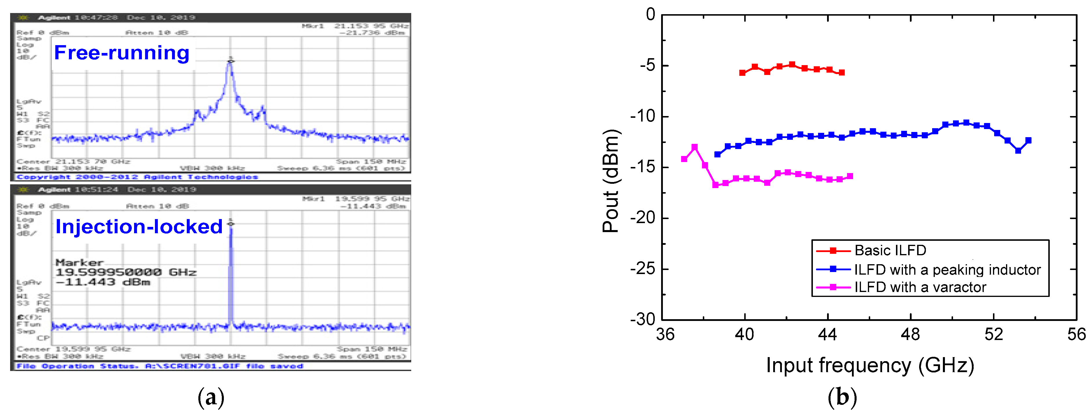
Figure 12 shows the measurement result of the ILFDs. Figure 12a shows the measured output spectrum in the free-running and injection-locked modes. It was observed that the output signal at 19.6 GHz was clearly locked to the injection signal of PLO = 0 dBm at 39.2 GHz. Figure 12b presents a comparison of the LR and output power of the three ILFDs at PLO = 0 dBm. The ILFD with a peaking inductor achieved the widest LR of 35.1% (19.4–26.9 GHz). The output power of the ILFD was no lower than −13.8 dBm over the LR.
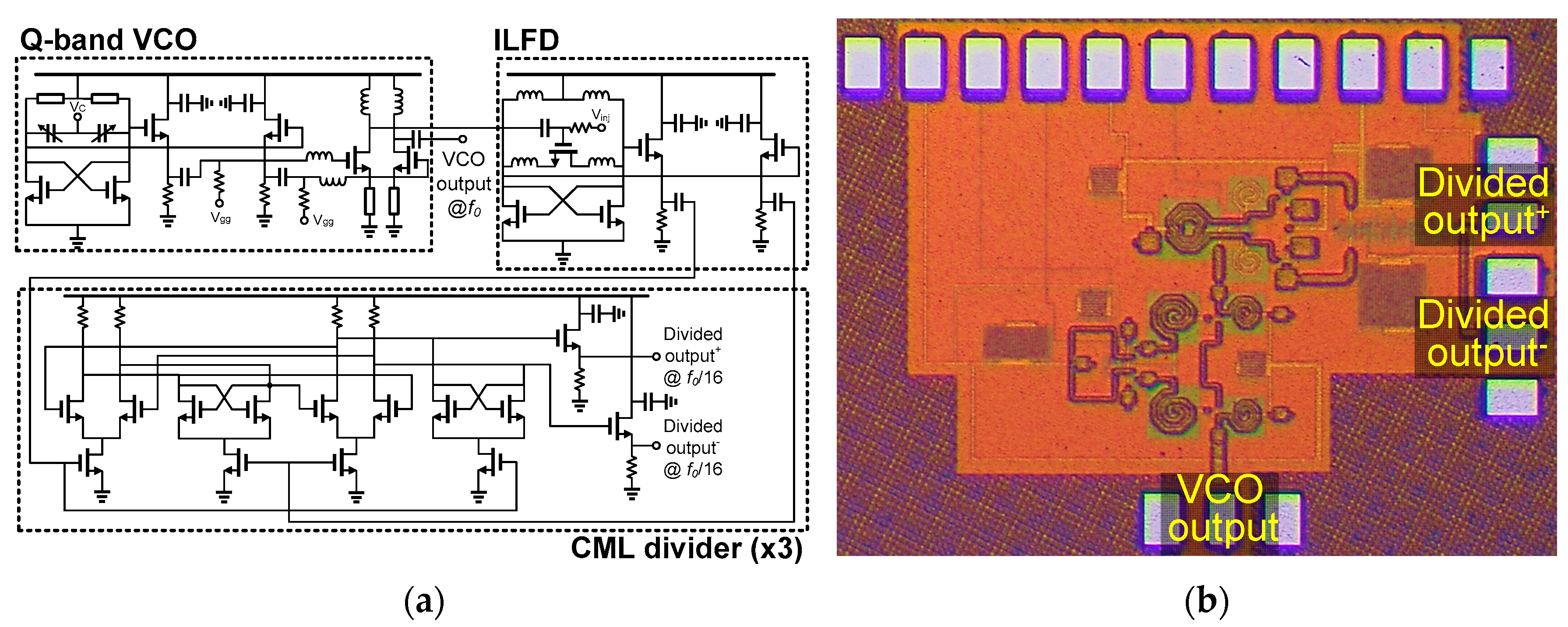
To achieve a sufficient frequency division ratio, the output of the ILFD was further divided by the subsequent CML dividers. Seven CML dividers were connected in cascade, so that the whole divider chain fulfilled a division ratio of 256 in the integrated receiver. To experimentally verify the operation of the divider chain, a reduced version of the LO test cut consisting of a Q-band VCO and a 1/16 divider chain shown in Figure 13 was tested. The divider chain was composed of the ILFD with a peaking inductor and three-stage CML divider employing a master-slave structure. One of the differential VCO output signals was monitored to check the oscillation frequency.
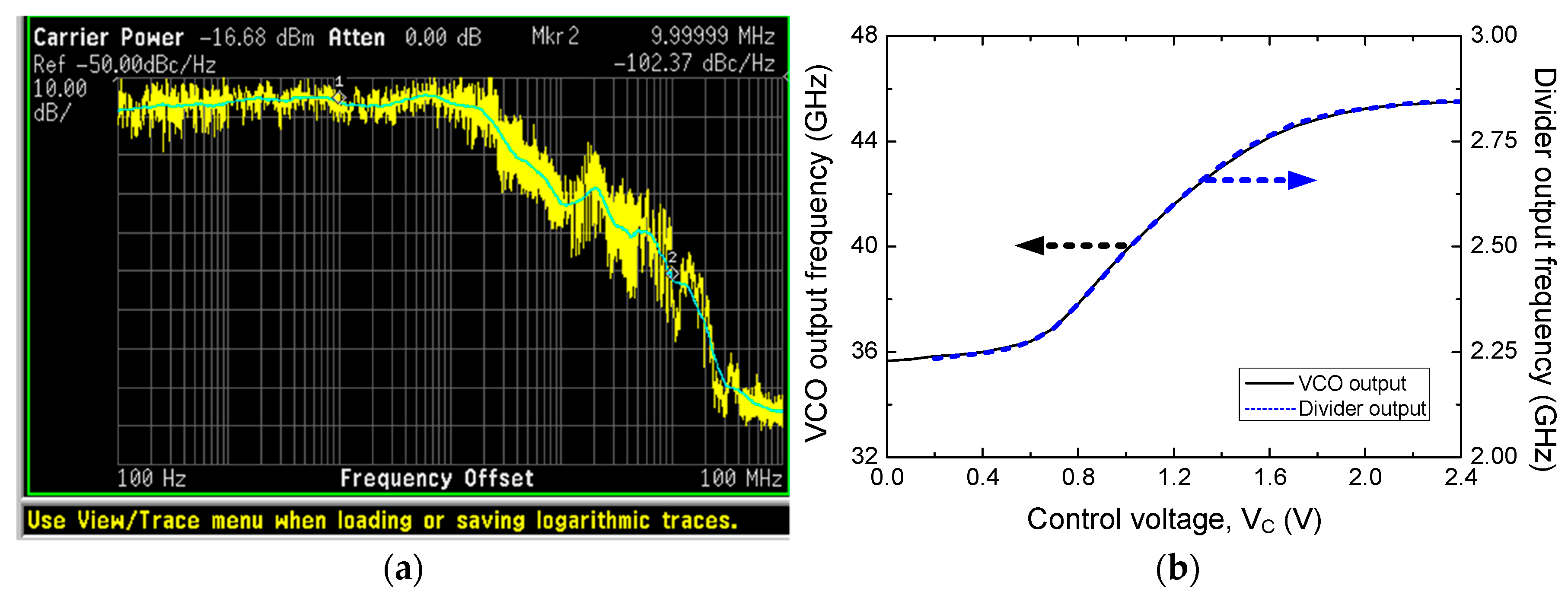
Figure 14 shows the measurement results of the Q-band VCO followed by a 1/16 divider chain. The phase noise of the divided signal was −102.37 dBc/Hz at 10 MHz offset as shown in Figure 14a. Figure 14b shows the output frequency of the VCO and the divider versus the VCO control voltage. It was observed that the frequency division by 16 was exactly performed.

4. Measurement of the Q-Band Image-Rejection Receiver

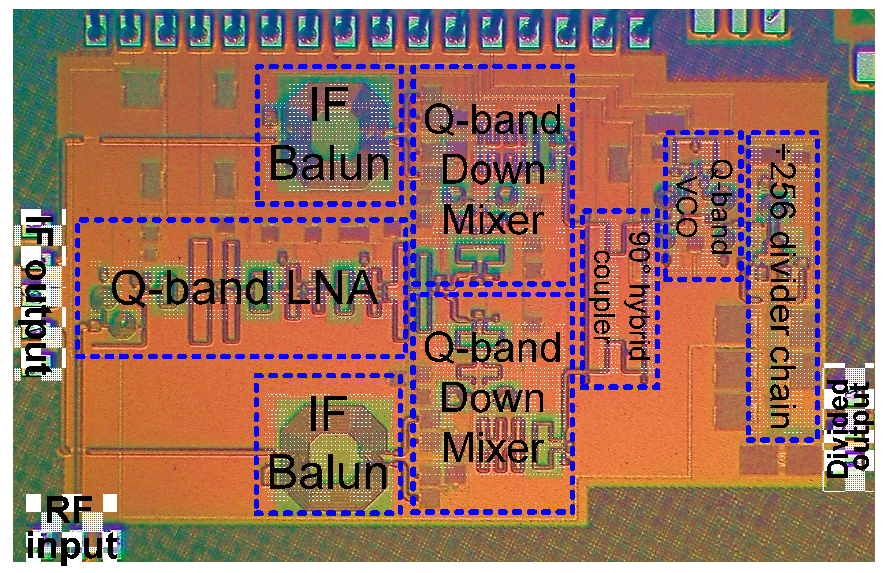
A Q-band image-rejection receiver integrated the circuit blocks described in Section 3 on a single chip, as shown in Figure 15. The chip area was 2.5 × 1.6 mm2 including the probing pads.
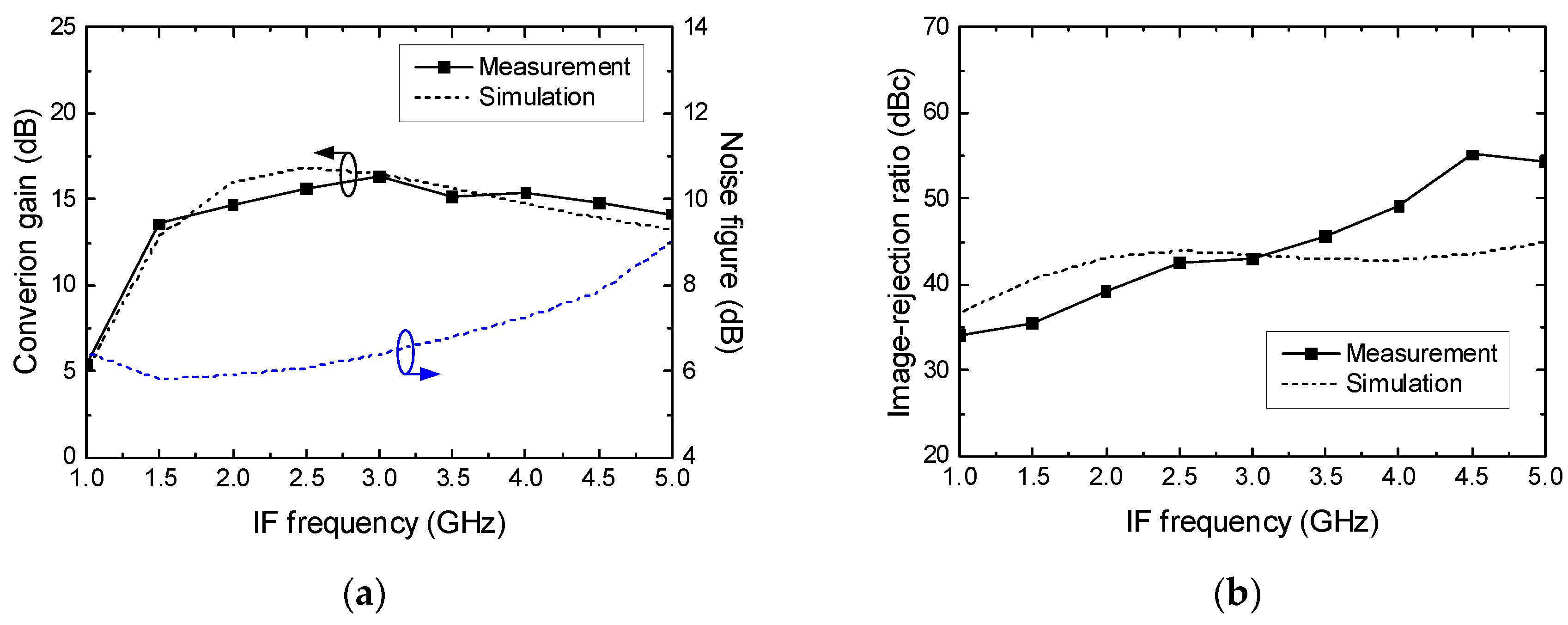
The measurement result of the image-rejection receiver is shown in Figure 16. The conversion gain was measured versus the IF frequency while the LO frequency was fixed at 40 GHz. As shown in Figure 16a, the receiver exhibited a peak conversion gain of 16.4 dB at 43 GHz and a 3 dB bandwidth of 3.5 GHz (1.5–5 GHz). The noise figure was simulated to be 5.8–7.8 dB over the 3 dB bandwidth. Figure 16b shows the measured IMRR, which ranged from 35.6 to 55.1 dBc over the same bandwidth. The input 1 dB compression power (IP1dB) was Ȓ28 dBm at the IF frequency of 2.5 GHz.
In Table 5, the performance of the Q-band image-rejection receiver is summarized and compared with those of previously reported silicon-based receivers in a similar frequency band. Compared with other image-rejection receivers, this work achieved a high IMRR at a reasonably low IF frequency below 5 GHz using the Hartley structure. It should be noted that a high IMRR was achieved in [13] by using a high IF frequency of 16 GHz. In addition, the LO circuit consisting of a VCO and a 1/256 divider chain was integrated in this work, which facilitated locking to a low-frequency LO reference.

5. Conclusions

In this paper, a Q-band image-rejection receiver was developed using a 65 nm bulk CMOS technology, which is relatively cost-effective and easily accessible. The Q-band receiver employing a Hartley architecture for a high IMRR integrates a Q-band LNA, two Q-band down-conversion mixers, a 90° hybrid coupler, two IF baluns, and an LO circuit. The integrated LO consists of a Q-band fundamental VCO followed by a 1/256 divider chain, which fulfills a high division ratio. This facilitates the LO locking to an external phase-locked loop (PLL). The Q-band image-rejection receiver exhibits a peak conversion gain of 16.8 dB and a high IMRR of 35.6 dB with IP1dB of −28 dBm. This receiver can be employed for future 5G mm-wave communication.

Author Contributions

Methodology, H.L. and S.J.; validation, H.L. and S.J.; investigation, H.L. and S.J.; resources, H.L. and S.J.; data curation, H.L. and S.J.; writing—original draft presentation, H.L. and S.J.; writing—review and editing, H.L. and S.J.; supervision, S.J.; project administration, S.J.; funding acquisition, S.J. All authors have read and agreed to the published version of the manuscript.

Funding

This work was supported by Institute of Information & communications Technology Planning & Evaluation (IITP) grant funded by the Korean government(MSIT) (2021-0-00260, Research on LEO Inter-Satellite Links).

Data Availability Statement

Not applicable.

Acknowledgments

The authors would like to thank the IC Design Education Center (IDEC), Korea for the chip fabrication and EDA tool support.

Conflicts of Interest

The authors declare no conflict of interest.

References

  1. Kim, S.; Kim, B.; Lee, Y.; Kim, S.; Shin, H. A 28 GHz direct conversion receiver in 65nm CMOS for 5G mmWave radio. In Proceedings of the International System-on-Chip Design Conference (ISOCC), Jeju, Korea, 6–9 October 2019; pp. 29–30. [Google Scholar]
  2. Wong, A.C.-W.; Devita, G.; Wu, S.-M.; Lauria, F.; Eid, M.; Illuromi, O.; Ogunkunle, S.; Modigliana, A. A 4Rx, 4Tx Ka-band transceiver in 40 nm bulk CMOS technology for satellite terminal applications. In Proceedings of the IEEE Radio Frequency Integrated Circuits Symposium (RFIC), Atlanta, GA, USA, 7–9 June 2021; pp. 211–214. [Google Scholar]
  3. Liu, X.; Yang, C.; Yang, Z.; Guo, Y.; Jin, J.; Shi, L.; Xu, Q.; Wu, L.; Zhou, J. Area-Efficient 28-GHz Four-Element Phased-Array Transceiver Front-End Achieving 25.2% Tx Efficiency at 15.68-dBm Output Power. IEEE Trans. Microw. Theory Tech. 2023, 71, 654–668. [Google Scholar] [CrossRef]
  4. Yuan, Y.; Li, N.; Zhou, J.; Gao, H.; Wang, S.; Lu, H.; Gu, Q.J.; Song, C.; Xu, Z. A Compact Ka-Band Eight-Element Four-Beam Receiver for Low-Earth-Orbit Satellite Communications in 65-nm CMOS. IEEE Microw. Wireless Tech. Lett. 2023, 33, 883–886. [Google Scholar] [CrossRef]
  5. Kim, H.-T.; Park, B.-S.; Song, S.-S.; Moon, T.-S.; Kim, S.-H.; Kim, J.-M.; Chang, J.-Y.; Ho, Y.-C. A 28-GHz CMOS Direct Conversion Transceiver with Packaged 2 × 4 Antenna Array for 5G Cellular System. IEEE J. Solid State Circ. 2018, 53, 1245–1259. [Google Scholar] [CrossRef]
  6. Lee, Y.; Kim, S.; Shin, H. A 24 GHz CMOS Direct-Conversion RF Receiver with I/Q Mismatch Calibration for Radar Sensor Applications. Sensors 2022, 22, 8246. [Google Scholar] [CrossRef] [PubMed]
  7. Shiramizu, N.; Nakamura, T.; Masuda, T.; Washio, K. A 24-GHz low-power fully integrated receiver with image-rejection using rich-transformer direct-stacked/coupled technique. In Proceedings of the IEEE Radio Frequency Integrated Circuits Symposium (RFIC), Anaheim, CA, USA, 23–25 May 2010; pp. 369–372. [Google Scholar]
  8. Fonte, A.; Plutino, F.; Moquillon, L.; Razafimandimby, S.; Pruvost, S. 5G 26 GHz and 28 GHz bands SiGe:C receiver with very high-linearity and 56 db dynamic range. In Proceedings of the 2018 13th European Microwave Integrated Circuits Conference (EuMIC), Madrid, Spain, 23 September 2018; pp. 57–60. [Google Scholar]
  9. Ma, Q.; Chung, H.; Rebeiz, G.M. A 4-channel 10–40 GHz wideband receiver with integrated frequency quadrupler for high resolution millimeter-wave imaging systems. In Proceedings of the 2018 IEEE MTT-S International Microwave Symposium (IMS), Philadelphia, PA, USA, 10–15 June 2018; pp. 883–886. [Google Scholar]
  10. Milner, L.E.; Harvey, J.T.; Parker, M.E.; Hall, L.T.; Rodriguez, M.C.; Heimlich, M.C.; Mahon, S.J. A 25 to 45 GHz SiGe receiver MMIC. In Proceedings of the 2016 11th European Microwave Integrated Circuits Conference (EuMIC), London, UK, 3–4 October 2016; pp. 548–551. [Google Scholar]
  11. Huang, M.-Y.; Chi, T.; Wang, F.; Li, S.; Huang, T.-Y.; Wang, H. A 24.5–43.5 GHz compact RX with calibration-free 32-56 dB full-frequency instantaneously wideband image rejection supporting multi-Gb/s 64-QAM/256-QAM for multi-band 5G massive MIMO. In Proceedings of the IEEE Radio Frequency Integrated Circuits Symposium (RFIC), Boston, MA, USA, 2–4 June 2019; pp. 275–278. [Google Scholar]
  12. El-Nozahi, M.; Amer, A.; Sanchez-Sinencio, E.; Entesari, K. A Millimeter-Wave (24/31-GHz) Dual-Band Switchable Harmonic Receiver in 0.18-μm SiGe Process. IEEE Trans. Microw. Theory Tech. 2010, 58, 2717–2730. [Google Scholar] [CrossRef]
  13. Li, G.; Ma, Q.; Rebeiz, G.M. A 20–44-GHz Image-Rejection Receiver With >75-dB Image-Rejection Ratio in 22-nm CMOS FD-SOI for 5G Applications. IEEE Trans. Microw. Theory Tech. 2020, 68, 2823–2832. [Google Scholar]
  14. Huang, M.-Y.; Chi, T.; Li, S.; Huang, T.-Y.; Wang, H. A 24.5–43.5-GHz ultra-compact CMOS receiver front end with calibration-free instantaneous full-band image rejection for multiband 5G massive MIMO. IEEE J. Solid State Circ. 2020, 55, 1177–1186. [Google Scholar] [CrossRef]
  15. Quadrelli, F.; Manente, D.; Seebacher, D.; Padovan, F.; Bassi, M.; Mazzanti, A.; Bevilacqua, A. A Broadband 22–31-GHz Bidirectional Image-Reject Up/Down Converter Module in 28-nm CMOS for 5G Communications. IEEE J. Solid State Circ. 2022, 57, 1968–1981. [Google Scholar] [CrossRef]
  16. Gao, L.; Rebeiz, G.M. A 20–42-GHz IQ Receiver in 22-nm CMOS FD-SOI With 2.7–4.2-dB NF and −25-dBm IP1dB for Wideband 5G Systems. IEEE Trans. Microw. Theory Tech. 2021, 69, 4951–4960. [Google Scholar] [CrossRef]
  17. Singh, R.; Mondal, S.; Paramesh, J. A Millimeter-Wave Receiver Using a Wideband Low-Noise Amplifier with One-Port Coupled Resonator Loads. IEEE Trans. Microw. Theory Tech. 2020, 68, 3794–3803. [Google Scholar] [CrossRef]
  18. Razavi, B. RF Microelectronics; Prentice Hall: Hoboken, NJ, USA, 2012. [Google Scholar]
  19. Hartley, R. Modulation System. U.S. Patent 1,666,206, 17 April 1928. [Google Scholar]
  20. Gilbert, B. A precise four-quadrant multiplier with subnanosecond response. IEEE J. Solid State Circ. 1968, 3, 365–373. [Google Scholar] [CrossRef]
  21. Sulivan, P.J.; Xavier, B.A.; Ku, W.H. Low voltage performance of a microwave CMOS Gilbert cell mixer. IEEE J. Solid State Circ. 1997, 32, 1151–1155. [Google Scholar] [CrossRef] [Green Version]
  22. Lee, S.-J.; Kim, B.; Lee, K. A novel high-speed ring oscillator for multiphase clock generation using negative skewed delay scheme. IEEE J. Solid State Circ. 1997, 32, 289–291. [Google Scholar]
  23. Castañeda-Aviña, P.R.; Tlelo-Cuautle, E.; De la Fraga, L.G. Phase noise optimization of integrated ring voltage-controlled oscillators by metaheuristics. AIMS Math. 2022, 7, 14826–14839. [Google Scholar] [CrossRef]
  24. Maggio, G.M.; Feo, O.D.; Kennedy, M.P. VCOs can be designed using ring-type, colpitts, and cross-coupled structures. IEEE Trans. Circ. Syst. I Fundam. Theory Appl. 1999, 46, 1118–1130. [Google Scholar] [CrossRef] [Green Version]
  25. Hajimiri, A.; Lee, T.H. Design issues in CMOS differential LC oscillators. IEEE J. Solid State Circ. 1999, 34, 717–724. [Google Scholar] [CrossRef] [Green Version]
  26. Razavi, B. Design of Integrated Circuits for Optical Communications; McGraw-Hill: New York, NY, USA, 2003. [Google Scholar]
  27. Alioto, M.; Palumbo, G. Model and Design of Bipolar and MOS Current-Mode Logic: CML, ECL and SCL Digital Circuits; Springer Science & Business Media: Berlin/Heidelberg, Germany, 2006. [Google Scholar]
  28. Tiebout, M. A CMOS Direct Injection-Locked Oscillator Topology as High-Frequency Low-Power Frequency Divider. IEEE J. Solid State Circ. 2004, 39, 1170–1174. [Google Scholar] [CrossRef]
  29. Cheng, J.-H.; Tsai, J.-H.; Huang, T.-W. Design of a 90.9% Locking Range Injection-Locked Frequency Divider with Device Ratio Optimization in 90-nm CMOS. IEEE Trans. Microw. Theory Tech. 2016, 65, 187–197. [Google Scholar] [CrossRef]
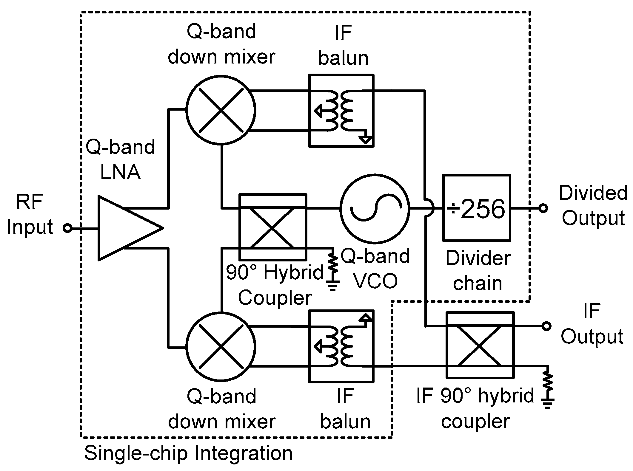
Figure 1. Block diagram of the Q-band image-rejection receiver.
Electronics 12 03069 g001
Figure 2. (a) Schematic diagram and (b) chip micrograph of the Q-band LNA.
Electronics 12 03069 g002
Figure 3. Layout of the (a) transmission line, (b) inductor, and (c) transformer.
Electronics 12 03069 g003
Figure 4. Measurement results of the Q-band LNA: (a) S-parameters and NF; (b) output power and power gain versus input power at 33.5 GHz.
Electronics 12 03069 g004
Figure 5. (a) Schematic diagram and (b) chip micrograph of the Q-band down-conversion mixer.
Electronics 12 03069 g005
Figure 6. Measurement of the Q-band down-conversion mixer: (a) conversion gain versus RF frequency with fLO = 40 GHz and PLO = 0 dBm, and (b) conversion gain and IF output power versus RF input power with fIF = 1 GHz, fRF = 41 GHz and PLO = 0 dBm.
Electronics 12 03069 g006
Figure 7. (a) Schematic diagram and (b) chip micrograph of the Q-band VCO.
Electronics 12 03069 g007
Figure 8. Measured oscillation frequency and output power of the Q-band VCO versus the control voltage.
Electronics 12 03069 g008
Figure 9. Schematic diagram of a basic Q-band ILFD.
Electronics 12 03069 g009
Figure 10. Schematic diagram of (a) ILFD with a peaking inductor and (b) ILFD with a varactor.
Electronics 12 03069 g010
Figure 11. Chip micrographs of the (a) basic ILFD, (b) ILFD with a peaking inductor, and (c) ILFD with a varactor.
Electronics 12 03069 g011
Figure 12. Measurement result of the ILFDs: (a) output spectrum in the free-running and injection-locked modes; (b) LR and output power at PLO = 0 dBm.
Electronics 12 03069 g012
Figure 13. (a) Schematic diagram and (b) chip micrograph of the Q-band VCO followed by a 1/16 divider chain.
Electronics 12 03069 g013
Figure 14. Measurement results of the Q-band VCO followed by a 1/16 divider: (a) phase noise at 10-MHz offset and (b) output frequency of the VCO and divider versus the VCO control voltage.
Electronics 12 03069 g014
Figure 15. Chip micrograph of the Q-band image-rejection receiver.
Electronics 12 03069 g015
Figure 16. Measurement of the Q-band image-rejection receiver: (a) conversion gain, noise figure, and (b) image-rejection ratio.
Electronics 12 03069 g016
Table 1. Parameter values of the Q-band LNA.
ParameterValueParameterValue
M1–M71 × 10 μmCdc, Cbypass880 fF
L1380 pHC1160 fF
L2460 pHCN8.8 fF
Table 2. Parameter values of the Q-band down-conversion mixer.
ParameterValueParameterValueParameterValue
M8, M92 × 20 μmR3, R4730 ΩC3203 fF
M10–M132 × 12 μmR5, R768 ΩCbypass880 fF
M14, M152 × 30 μmR6, R892 ΩCIF5 pF
RG5 kΩLS240 pH
R1, R2340 ΩC2139 fF
Table 3. Parameter values of the Q-band VCO.
ParameterValueParameterValue
M16, M171.5 × 12 μmL5, L6250 pH
M18, M191.5 × 20 μmL7, L8195 pH
M20, M213 × 20 μmCbypass880 fF
RG5 kΩCvar51.6–146 fF
R9, R10100 Ω
Table 4. Parameter values of the ILFDs.
ParameterValueParameterValue
M22, M23, M27, M28, M32, M33 3 × 13 μmLres290 pH
M24, M29, M342 × 24 μmLpeak120 pH
M25, M26, M30, M31, M35, M363 × 20 μmCbypass1.4 pF
RG5 kΩCvar41–167 fF
R11–R1680 Ω
Table 5. Performance summary and comparison.
Ref.ProcessRF Freq. (GHz)ArchitectureCG 1
(dB)
NF 2
(dB)
IP1dB
(dBm)
IMRR
(dBc)
Pdc
(mW)
[6]65 nm CMOS22.5–26.1LNA + Mixer + AMPIF 3 + AMPLO 4 + PPFLO 531.54.8−35.2-127.44
[9]0.12 μm SiGe10–40LNA + Mixer + VGAIF 6 + ×4 + AMPLO 4396.8−33-130
[10]0.13 μm SiGe25–45LNA + Mixer + ×3 + AMPLO 4215-30-
[11]45 nm SOI CMOS24–44LNA + Mixer + AMPIF 3 + AMPLO 435.23.2−25.53260
[13]22 nm SOI CMOS20–44LNA + Mixer + AMPIF 3 + AMPLO 428.53.3−257570
[16]22 nm SOI CMOS19.5–42LN-VGA + mixer + LPF
+ AMPIF 3 + AMPLO 4 + IQGEN 7
25.32.7−23-102
[17]65 nm CMOS26.5–32.5LNA + Mixer + BuffIF 8 + AMPLO 4 + PPFLO529.55.3−28-33
This work65 nm CMOS41.5–45LNA + Mixer + VCO + 1/256 divider16.45.82835.691.9
+ 294 (divider chain)
1 Maximum conversion gain over the bandwidth. 2 Lowest NF over the bandwidth. 3 IF amplifier. 4 LO amplifier. 5 LO poly phase filter. 6 IF variable gain amplifier. 7 I-Q generator. 8 IF buffer.
Disclaimer/Publisher’s Note: The statements, opinions and data contained in all publications are solely those of the individual author(s) and contributor(s) and not of MDPI and/or the editor(s). MDPI and/or the editor(s) disclaim responsibility for any injury to people or property resulting from any ideas, methods, instructions or products referred to in the content.