Article

A Self-Triggered Digitally Assisted Hybrid LDO with 110 ns Settling Time in 65 nm CMOS

Department of Electric and Electronic Engineering, Chung-Ang University, Seoul 06974, Republic of Korea
*
Author to whom correspondence should be addressed.
Electronics 2023, 12(15), 3215; https://doi.org/10.3390/electronics12153215
Submission received: 26 June 2023 / Revised: 21 July 2023 / Accepted: 24 July 2023 / Published: 25 July 2023
(This article belongs to the Section Circuit and Signal Processing)

Abstract

:
This article presents a self-triggered digitally assisted hybrid low-dropout regulator (LDO). The proposed architecture uses an analog LDO for steady-state operation and a digital LDO to track large output current changes. The dual loop has a loop controller for coherent operation, and the digital loop is only triggered when there is a large load step. Therefore, the proposed LDO inherits some of the advantages of both parts. It achieves a high power supply rejection ratio (PSRR) from the analog part. The digital loop has a faster settling time and consumes less static power than the analog loop. In this design, the maximum load is 200 mA. For heavy load conditions, PSRR is −40 dB at 1 MHz. The quiescent current is 200 μA. The undershoot/overshoot with the corresponding settling time measured under a load current step of 200 mA/10 ns are 82 mV/89 ns and 112 mV/110 ns, respectively. The proposed LDO achieves a competitive 4.48 ps figure of merit. In the TSMC 65 nm process, the active area is approximately 0.027 mm2.

1. Introduction

With the progression of technology, an increasing number of functionalities can be incorporated into a singular chip, necessitating energy-efficient system-on-chip (SoC) solutions for the most sophisticated electronic devices. In modern electronic products, the power management integrated circuit (PMIC) [1] is particularly apt for applications requiring low power consumption and high levels of integration. The contemporary PMIC approach calls for reducing the power supply voltage to diminish power consumption while simultaneously incorporating various analog, digital, and RF modules onto a single silicon substrate, i.e., SoC, alongside multiple voltage regulators to cater to diverse requirements [2]. Over the past few decades, there has been an enormous demand for SoC modules with varying regulated voltages and load specifications. Moreover, positioning the required power management module as close to the load as feasible would prove beneficial in achieving optimum performance, making on-chip implementation the ideal solution to this issue.
Figure 1a presents the basic PMIC scheme of SoCs, which amalgamates a switching DC–DC converter and a low-dropout regulator (LDO) to produce multiple clean power supplies across the entire chip. Nevertheless, this traditional PMIC becomes profoundly susceptible to the parasitic effects of complex power lines. For instance, parasitic inductance associated to a long power line can cause excessive ripple voltage, whereas parasitic resistance can lead to a resistance drop in the voltage perceived by the modules. Applying a filter capacitor near each module’s power supply pin can attenuate the influence of parasitic inductance. However, such an addition significantly complicates the chip design and augments the cost. Moreover, the fundamental scheme remains impacted by the resistive voltage drop.
Figure 1b presents the recent PMIC scheme for SoC, where an LDO is integrated within the module. Due to this integration, the parasitic effect between the LDO and modules is almost non-existent. The integrated LDO typically demands an extensive drive capability and rapid transient response. For instance, a digital module packed with a significant number of swiftly switching devices will induce substantial and abrupt changes in load current when the devices are dynamically toggled on and off. Given that a complex SoC necessitates multiple LDOs to power various modules, the dimensions of the LDO should be minimized. In summary, to seamlessly integrate with all modules, the LDO needs to have a high output current capacity, a swift transient response, and occupy a small chip area, and it should also provide the high PSRR performance demanded by RF/analog modules.
Analog low-dropout regulators (ALDOs) [3,4,5,6,7,8,9], as illustrated in Figure 2a, have been extensively studied and developed for several decades and are commonly utilized as on-chip voltage regulators. An ALDO comprises an error amplifier (EA) and a large pass transistor, providing a well-regulated, noise-free output voltage with an impressive PSRR capability. This makes ALDOs ideal for powering noise-sensitive analog/RF circuits alongside their low static current performance. However, the downsides of ALDOs have become apparent with the advancements in CMOS process scaling, proving that they need to lend themselves better to the benefits of this scaling. They are incompatible with standard digital design flows. Further complicating matters, the reduction in power supply voltage and inherent gain of the transistor adds complexity to the analog circuit design, necessitating significant design work.
To address these issues with traditional ALDOs, digital LDOs (DLDOs), shown in Figure 2b [10,11,12,13,14,15,16,17,18], have been proposed. These innovative designs include a comparator, a shift register, and a bank of pass transistors. DLDOs demonstrate scalability, and their design allows the incorporated pass transistors to operate near or below the threshold voltage, unlike their ALDO counterparts. This scalability allows for synthesizing DLDOs into other digital function blocks within SoCs designs, facilitating easier integration. Various digital controller algorithms or asynchronous structures have been developed, targeting rapid transient response times and low static power consumption. Despite these advancements, DLDOs suffer from inherent quantization errors, leading to low accuracy, and they possess a narrow range of load current. This poses challenges in balancing speed and power.
Table 1 encapsulates a comparative analysis between analog low-dropout regulators and digital LDOs. DLDOs, aided by the pass transistor operating in shutdown and linear (resistance) modes, can achieve ultra-low dropout voltage. Technological advancement fosters the digital loop’s portability and reduces its power consumption, resulting in a superior area efficiency compared to ALDOs. Additionally, DLDOs exhibit a rapid settling time. Nevertheless, DLDOs are not devoid of shortcomings. Their fundamental limitations stem from a poor PSRR and a substantial output ripple. When pass transistors function in a linear mode, they operate as parallel resistors between the input and output of the DLDO, causing any input noise to directly couple to the output. This issue is further exacerbated in digital architectures due to their susceptibility to output ripple. Conversely, ALDOs avoid this issue as the error amplifier (EA) continuously drives the pass transistor with infinite resolution, mitigating the output ripple. Recent studies [19,20,21,22,23,24,25,26,27,28] have unveiled various hybrid topologies that fuse the benefits of both analog and digital control mechanisms. However, a pioneering attempt to connect an analog LDO and a digital LDO directly in parallel [19] underscored that a failure to adequately address the load-current-sharing issue could lead to a complete loss of the hybrid topology’s advantages. This reveals the necessity for an advanced control scheme that harmoniously balances both loops, designating one loop as dominant and the other as subordinate.
An analog-assisted digital LDO (AA-DLDO) introduced in [22] brought transient improvements, a diminished power consumption, and a reduced load capacitor (CL). Nevertheless, it employs dead zone control to eradicate limit cycle oscillations, compromising voltage accuracy. Further reports [24,25] of an AA-DLDO illustrated a scenario where the digital controller served as the primary controller, indicating that the additional power could be redundant in a steady-state situation. Moreover, the output voltage proved to be susceptible to switching noise, and the transient response time was inherently constrained by the clock cycle.
In the case of the dual-loop hybrid LDO [27], it employed a similar hybrid control approach, albeit with a complex loop controller that consumed a significant amount of power. Even with the application of an asynchronous digital controller, the transient performance of an event-driven DLDO with a residual tracking loop [23] was found to be poor. The modular hybrid LDO [26], on the other hand, essentially used the resources of two LDOs to accomplish a single task. Although this improved the PSRR, it resulted in unnecessary consumption and required an external clock to drive the digital cells.
In order to fully leverage the potential of the hybrid LDO, this paper proposes a self-triggered digitally assisted hybrid LDO (DA-HLDO). The LDO achieves a fast transient load response with a high PSRR and fast settling time without the external clock. Section 2 describes the proposed DA-HLDO architecture and working principle. Section 3 introduces the circuit implementation of various functional blocks. Section 4 presents the measurement results and discussion to verify the performance of DA-HLDO, and the conclusion is presented in Section 5.

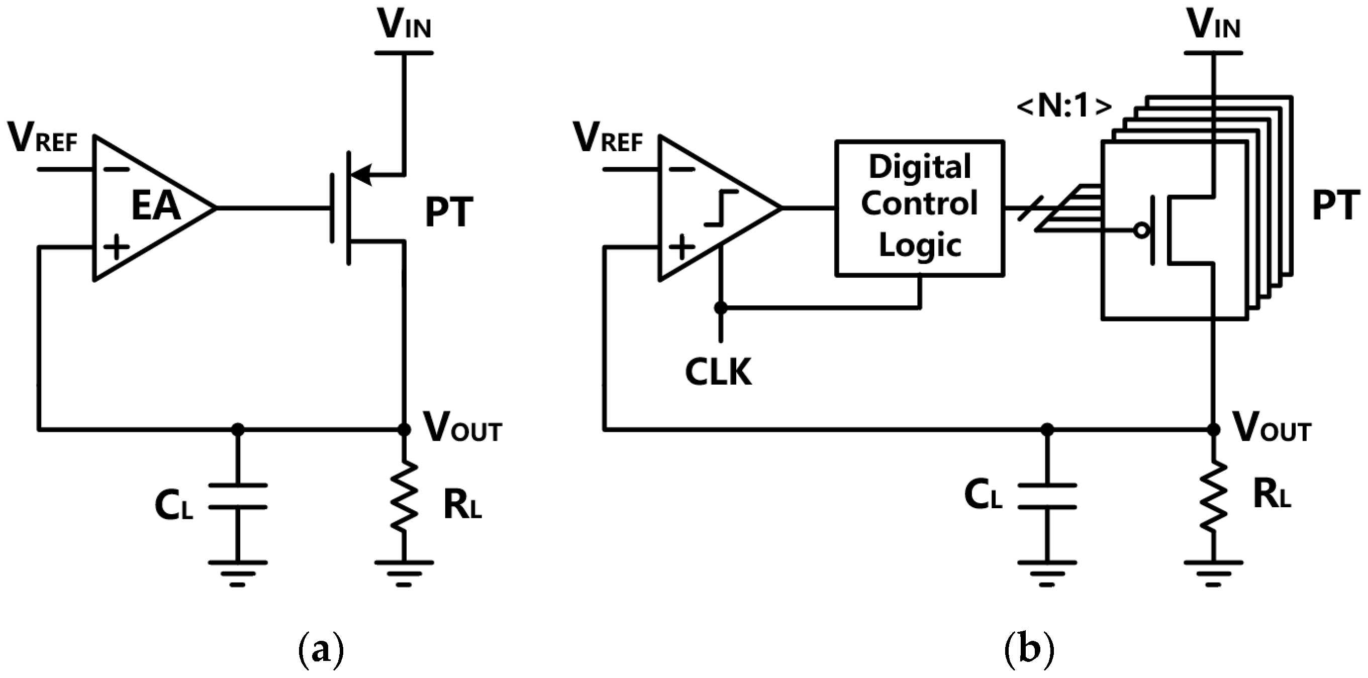
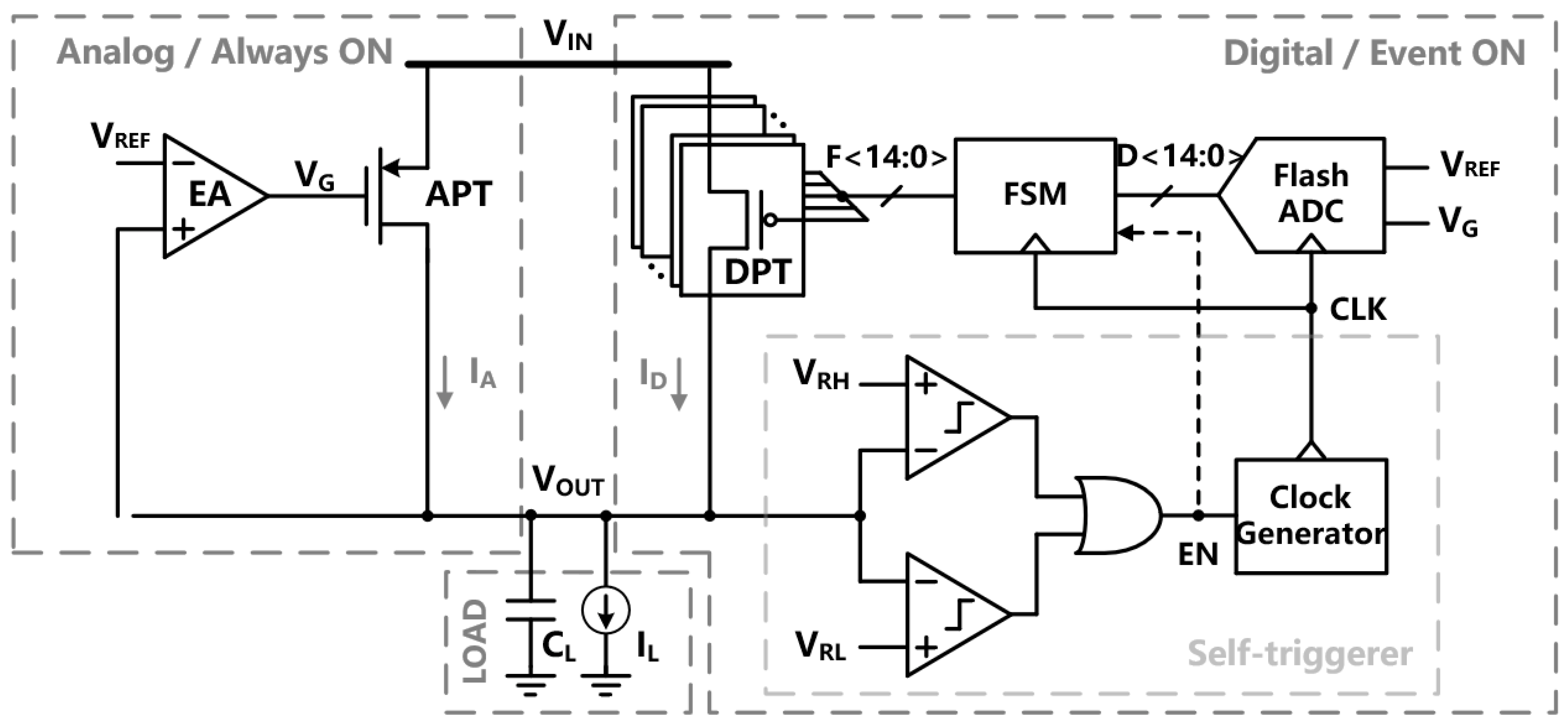
2. Proposed Architecture

In the proposed DA-HLDO model, the distinctive capabilities of both ALDO and DLDO are fully exploited. Specifically, ALDO is deployed for precise, fine-tuning control, while DLDO is reserved for broader, coarse tuning. This allocation of roles is sensible because the pass transistor in the ALDO, which is persistently driven by an error amplifier (EA), exclusively modulates minor variations in output voltage. Simultaneously, with the pass transistor operating in off and linear modes, the DLDO can realize an ultra-low dropout voltage. Continual advancements in process scaling lead to a portable digital loop that consumes less power. This digital loop handles the majority of load current while preserving area efficiency. Its inherent advantage in switching capability results in a rapid transient response. Therefore, in steady-state conditions, the preference is for analog operation, whereas during significant transient steps beyond the analog operation’s scope, digital operation proves to be more beneficial.
In contrast, the AA-DLDO structures, as seen in references [24,25], employ a DLDO as the primary controller and an ALDO as a secondary or ‘slave’ controller. This configuration, where DLDO remains constantly active, consequently leads to an increased static power consumption and higher levels of switching noise. Additionally, it necessitates the deployment of a top-level controller to manage the ALDO’s precise participation as a slave and to balance the resource distribution between the two loops. The analog control scheme is recognized for its superior static performance due to its inherent continuity and static nature. On the other hand, the digital control scheme shows a better performance in dynamic scenarios because it is fundamentally dynamic and is based on switching. This means the DA-LDO [20,21] is more practical for implementation than the AA-LDO. The DA-LDO concurrently harnesses the advantages of both ALDO and DLDO while mitigating their limitations.
The design of the proposed DA-HLDO strategically capitalizes on the precision of analog control and the swift transient response of digital control, resulting in an optimized performance. During steady-state operations, the digital control scheme is deactivated, allowing the analog control scheme to provide rigorous regulation, low idle current, an absence of switching noise, and a limitation on periodic oscillations at the output. However, during a transient event, if a substantial load change exceeds the range of the analog control, the digital control scheme is activated in response to the event. This method not only conserves the power consumption of the digital circuit, but it also ensures that the response time is no longer confined by the clock cycle.

2.1. Architecture of the DA-HLDO

The proposed LDO architecture is shown in Figure 3. It mainly comprises two parts: an ALDO used to track small load changes continuously and a DLDO activated when a large output voltage change occurs. The ALDO consists of a folded cascode error amplifier and an analog pass transistor (APT). The DLDO comprises a trigger composed of two event-driven comparators and a clock generator, a controller comprising a flash ADC (analog-to-digital converter), a finite state machine (FSM), and a digital pass transistor (DPT) bank.
The EA acts as the main controller in this hybrid scheme and continuously controls the APT to sample the output voltage directly and through APT to produce a continuous analog current (IA). The digital controller is a slave controller that provides discrete digital current (ID) through a 15-bit DPT array. The APT contributes 1 mA–50 mA of load current, and the part exceeding 50 mA (50 mA–200 mA) is contributed by fifteen 10 mA DPTs.
In this system, the ADC is structured into two main components—an event-driven ADC and a flash ADC, each rendering unique functionalities. The event-driven ADC is designed to incessantly monitor the VOUT, ensuring swift detection and reaction to transient events. Upon the identification of these transients, the digital part is promptly activated. In parallel, the flash ADC is responsible for comparing the VG to VREF, thus guaranteeing the stability of the DA-HLDO within a certain state. It is crucial to emphasize that VG is dynamically tailored according to the load current and the readings from the EA. The twofold function of the ADC, facilitating rapid responses by monitoring VOUT and precision by comparing VG, underscores the key advantage of our proposed architecture.
Two event-driven comparators are used to sense the output voltage VOUT. The output of the two event-driven comparators is passed through an OR gate. Whenever VOUT falls outside the range defined by the low threshold voltage (VRL) and the high threshold voltage (VRH), an enable signal (EN) is produced, which then triggers the clock generator. This, in turn, generates the clock signal for the flash ADC and FSM. In this way, two comparators and an OR gate constitute an under/overshooting detector, and the clock signal triggered by the EN signal becomes the digital controller’s switch.
After the initial rising edge of the clock signal, the digital controller is fully activated. The 15-bit code generated by the flash ADC through only one comparison is transmitted to the DPT through the FSM, and the required number of pass transistors will be on/off. The counter in the FSM will generate a specific delay time after one comparison to reduce the number of unnecessary comparisons and provide response time for VOUT. After several delay times, if VOUT does not return within VRH and VRL, compare again. This type of algorithm allows DLDOs to reach quickly and correctly. Theoretically, a 100 ns current step from minimum to maximum (maximum to minimum) can return VOUT to a stable state within ten clock cycles, the DLDO is shut down, and the ALDO continues to perform fine-tuning.
The proposed digitally assisted hybrid solution provides an area-efficient current transmission by delivering most of the load current. At the same time, the self-triggered scheme delivers a well-regulated noise-free output voltage by freezing the digital load current and adjusting the analog load current and uses a self-generated clock and flash ADC to achieve a settling time of less than 110 ns, maintaining the PSRR performance of the ALDO.

2.2. Static and Dynamic Performance

The FSM is shown in Figure 4. The proposed digital algorithm can handle every load condition with a high efficiency and a low overhead.
Our finite state machine (FSM) operates based on three states, namely S0, S1, and S2, which represent ‘digital off’, ‘digital on with comparing mode’, and ‘digital on with passing and freezing mode’, respectively. The transitions between these states are governed by two input signals, EN and CT. EN is the output signal from the event-driven ADC, indicating a detection of VOUT, whereas CT is a signal derived from the clock cycles counted by the counter in the FSM. For input EN, the digital controller detects the event-driven ADC output code. When ADC output is EN = 0, the last ADC output code freezes and the digital part’s sleep mode is maintained, which is defined as S0. When EN = 1, the digital part is activated, and the flash ADC starts to compare, defined as S1. For input CT, the counter in FSM starts counting on the second falling edge of the clock signal (CT = 0), passes the flash ADC’s comparison result to the DPT, and freezes until a new falling edge is generated, defined as S2. If VOUT returns within the reference boundary (EN = 0), the state transforms to S0, and the digital part shuts down. If VOUT is still outside the reference boundary (EN = 1), FSM keeps the previous comparison result frozen until the rising edge occurs (CT = 1) after several clock delays and returns to S1. If VOUT is still outside the reference boundary (EN = 1), the FSM will keep the previous comparison result frozen until a rising edge occurs after a few clock delays (CT = 1). The state returns to S1, and the flash ADC restarts the comparison. When the rising edge ends and the falling edge occurs after the clock delay (CT = 0), S2 is returned to again to pass the new comparison result to DPT and start a new round of counting. FSM repeats in this way until VOUT stabilizes within the boundary (EN = 0), and the analog loop works alone to become a steady state (S0). To further analyze the FSM in, a timing diagram for a current step is presented in Figure 5. The load current (IL) changes from a light load (IL = 1 mA) to a heavy load (IL = 200 mA).
In the beginning, the FSM stays in S0. According to the number of DPTs turned on, as IL is very small, only the APT in the ALDO is activated and adjusted. Then, the fast-rising IL causes VOUT to drop rapidly. When VOUT drops rapidly under VRL, EN = 1, and the FSM enters S1. In this case, the DLDO is triggered, and an EN signal is generated. This signal causes the clock generator to generate the clock signal.
In S1, after a large load change, DLDO is turned on due to clock generation. Then, during a clock cycle of FSM inherent response period, CT = 0, FSM reaches S2 and maintains the previous code. A rising edge occurs after one clock cycle, CT = 1, the flash ADC is activated for one comparison, and the output of the flash ADC is changed compared to the previous code. A falling edge occurs when the comparison is completed, CT = 0, and FSM enters S2. The counter starts counting, passing the new 15-bit thermometer code to the DPT, and freezing. After the three clock cycles’ counting time ends, CT = 1, and it detects that VOUT has not yet entered the VRL, so it returns to S1. The flash ADC performs the comparison again. After the comparison is completed, following the above steps, the FSM returns to S2. During the counting time, VOUT returns to the boundary, EN = 0, and the clock signal is no longer generated. FSM enters S0 and shuts down DLDO.
In the next case, VOUT has stayed the same for a period of time in a state where only the ALDO is working, and the FSM remains in the S0 state. This time, the fast-falling IL causes VOUT to rise rapidly. It is still because of the slow response of the analog loop that VOUT exceeds the VRH. The event-driven ADC detects that VOUT has left the range and performs the same algorithm as the above sequence. This time, IL has not dropped to the minimum value after one comparison because the DPT is completely turned on under heavy load conditions. However, too many DPTs are turned off, causing VOUT to fall below VRL. When returning to the VRH range and falling out of the VRL range again, EN = 0, and 15 DPTs turn on while DLDO is turned off. With falling out of VRL, the above S0, S1, S2, S1, and S2 steps should be followed. After one re-comparison, the flash ADC finds the correct 15-bit thermometer code, and VOUT returns to the reference boundary. The DLDO is turned off, and the ALDO performs fine-tuning in a steady state.
The introduction of the CT signal, or delay, is primarily because the flash ADC can, with only a single comparison, rapidly determine the number of DPTs that need to be activated. Instituting a specific delay time prevents unnecessary repeat comparisons and voltage oscillations due to minor current changes. Not only does reducing the number of comparisons decrease current consumption and reduce voltage oscillations, but it also optimally harnesses the benefits of the flash ADC.
Due to the FSM-based self-triggered digital controller, the analog loop regulates VOUT in a steady state, while the digital loop is only enabled under large load current variation. Therefore, DA-HLDO has high PSRR, fast response time, and no ripple on LDO output.

2.3. Power Supply Rejection Ratio

PSRR refers to the amount of voltage ripple at the output of the LDO from the input voltage. However, as mentioned in the above analysis, the PSRR performance comes from the ALDO and is proportional to the gain of the ALDO:
P S R R =   20 l o g V I N , R P L V O U T , R P L     A E A
where VIN,RPL and VOUT,RPL are the input ripple and output ripple, and AEA is the gain of the EA. In the analog topology, as load current IL increases, the PSRR will decrease, but the difference is less than 1/10. Due to the participation of DLDO in the hybrid topology, as IL increases, the DPT conduction current will increase. Under light loads, the analog part dominates. The DA-ALDO has a reasonably fair supply noise rejection capability due to the high bandwidth of the analog loop and the dominant pole being placed at the output. Under heavy loads, the digital part dominates, and the PSRR performance falls back to that of a conventional digital LDO. The loss in the resulting lowest PSRR performance at maximum load compared to the highest PSRR provided by ALDO at the lightest load is:
P S R R L O S S =   20 l o g I D I A V I N V O U T 1  
where IA and ID are the load currents of the analog power transistor and digital power transistor, where IL = IA + ID. Through the above formula, when VIN and VOUT are unchanged, increasing IA can reduce PSRRLOSS, but excessively increasing IA will reduce area efficiency. By weighing response time, area efficiency, and PSRR performance, the hybrid architecture proposed in this paper sets IA to 50 mA and PSRR loss to 23 dB. Through a 60 dB high-gain EA, DA-HLDO has an extremely high PSRR under light load conditions. Even though some PSRR is lost under heavy load conditions, it still has competitiveness in noise-sensitive modules such as RF/analog.
The simulated PSRR is plotted in Figure 6. Under light loads, the analog part dominates. Due to the high gain of the analog part, the DA-HLDO achieves more than a 56 dB supply rejection at low frequency and a 57 dB rejection up to 1 MHz. Under heavy loads, although the digital part is responsible for 3/4 of the load current, the DA-HLDO achieves a 45 dB supply rejection at low frequency and a 40 dB rejection up to 1 MHz. Compared with conventional DLDOs, the proposed digitally assisted LDO can improve the PSRR performance by introducing analog circuits into the system. Although the hybrid LDO [27] solves a part of the serious loss of PSRR performance under heavy load problem, it uses a large area of power transistors. The control method is complicated, and the external clock is used, which requires additional components, and the current consumption is relatively large because the digital part is always working.

3. Implementation of Core Circuit

In this section, the detailed circuit implementations of various core functional blocks of the proposed DA-HLDO are introduced. Design considerations are first validated based on which appropriate resources are allocated.

3.1. Analog Error Amplifier

A folded cascode error amplifier is employed, as shown in Figure 7. M1–M11 form a folded cascade stage. Stability problems can arise due to the large parasitic changes of the segmented transistors. To mitigate this issue, a source follower buffer is added between the folded cascode amplifier and the pass transistor. The buffer is realized by M12 and M13. The source follower has a low input parasitic capacitance and a low equivalent output impedance. In the folded cascode stage, M2 and M3 are identical. From M4 to M11, the transistors of the left branch are also identical to the transistors on the right branch. The small signal gain is defined as [27].
V o V i = g m 2 · g m 9 + 1 r o 9 g m 9 + 1 r o 9 + 1 r o 11 × [ g m 9 · r o 9 · r o 11 / / r o 2 + r o 9 + r o 11 / / r o 2 ] / / [ g m 7 · r o 7 · r o 5 + r o 7 + r o 5 ]     g m 2   · R o 2
where gmx and rox are the transconductance and the output resistance of MX; x denotes the index; and Ro2 is the equivalent output resistor of the folded cascode stage.
The gain of the voltage buffer is very close to unity with a single pole ωpg. Thus, the transfer function of the EA can be obtained by the following:
V o V i ( s )   =   g m 2 · R o 2 1 + s / ω p g 1 + s / ω p 2
where ωpg = 1/(Rbf Cp,gate) and ωp2=1/(Ro2 Cp2). Rbf denotes the equivalent output resistor at the buffer stage, and Cp2 is the total parasitic capacitance at node Vo2, while Cp,gate is the gate capacitance of the pass transistors. In this design, Rbf ≈ 1/gm12 represents a small resistor about 8 kohm.

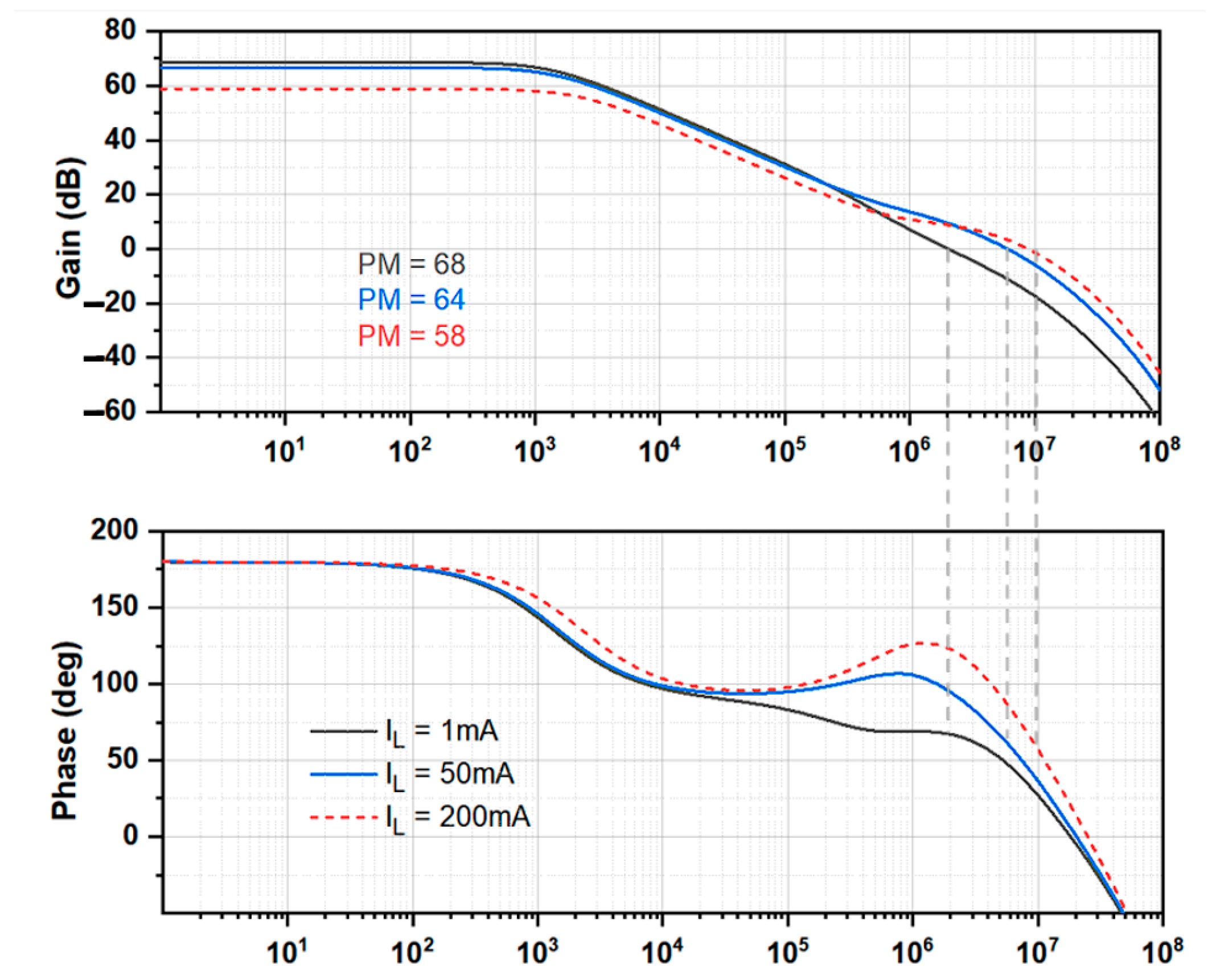
3.2. Stability Analysis

The analog loop consists of three poles and one zero. ωpo and ωpg are regarded as the dominant output pole and buffer output pole, respectively. The buffer output pole is pushed beyond the unity-gain bandwidth of the LDO loop since the buffer output impedance is small.
Under different load currents, the locations of ωpo and ωpg change significantly. For a light load, ωpo is a low-frequency pole, and ωpg is located at high frequencies. In this case, ωpo and ωpg are widely separated. However, ωpo and ωpg will approach closer to each other for a heavy load. Hence, the heavy load is the worst case for loop stability.
A pole-zero compensation scheme is used to introduce a zero in the loop that compensates for the EA’s second pole, as shown in Figure 7 [29]. The pole generated from this R-C network is at high enough frequencies to impact the loop stability.
The resistor and capacitor are RC = 20 kΩ and CC = 12 pF, where RC is the fixed resistance used along with a pole–zero tracking scheme. Figure 8 shows the simulation results for the magnitude and phase of the loop gain under different loading conditions. fpo varies in the kHz range, and fpg is located in the MHz range. In this design, fp2 and other high-frequency poles are over 400 MHz. The phase margin for the worst scenario is approximately 58°. Therefore, the analog loop stability can be guaranteed throughout the entire load current range.

3.3. Event-Driven Comparator

Our design includes discrete sets of comparators for both VOUT and VG, enabling an effective monitoring of these parameters. Speed is a shared critical requirement for all comparators. However, the VOUT comparators necessitate precise matching, while the VG comparators in flash ADC require a minimized input capacitance. As illustrated in Figure 9, the NMOS input comparator employs a PMOS active load, which is cross-coupled. This inherent positive feedback facilitates an increase in speed. This same topology is applicable to PMOS input comparators but with NMOS cross-coupled active loads instead.
Two event-driven comparators are employed to detect if VOUT falls within the VRH and VRL range, as depicted in Figure 3. This is facilitated by the unequal sizing of the input transistors, which introduces an offset voltage, Δ, of approximately 25 mV (with a P/N ratio of 2:3). This offset value is strategically selected to ensure a balance between a quick transient detection (necessitating a small offset) and the adaptability to process variations, mismatch, and transient noise (requiring a larger offset to avoid false triggering). The optimal offset value was identified via a comprehensive simulation. To accurately define the offset voltage in light of process variations, the input transistors must be suitably large and well-matched in the layout to mitigate any adverse effects.

3.4. Clock Generator

A current-starved ring oscillator with an enable pin EN is utilized as the controlled clock generator. The enable signal is applied to a standard NAND cell inside the ring oscillator, and the other cells are all current-starved inverter cells, as shown in Figure 10. When the EN input is high, the NAND unit is ultimately an inverter, and when the EN input is low, the NAND unit blocks the signal and stops clock generation. The CLK signal is generated from the output of the NAND unit, as shown in Figure 10. The NAND gate ensures that CLK is always 0 when the digital controller is disabled (EN = 0). In this way, once EN changes from zero to one, CLK will always change from zero to one as the first rising edge of the clock. Therefore, all digital parts can be started after a rising edge. Compared with the previous AA-HLDO work, a shorter response time has been achieved.
The oscillation frequency of the ring oscillator is determined by the combined delay of the inverters, including both propagation delay and output load. The total delay (td) of a single current-starved inverter cell is much larger than that of the NAND cell, and the total delay around the loop is approximately 4 td. The generated clock has a frequency of approximately 100 MHz.
For ring oscillator-based clock generators, process, voltage, and temperature (PVT) variations are significant. However, the frequency of the clock is affected by temperature (20 MHz clock difference occurred in the worst case) due to the digital loop set up, and finished working within ten clock cycles in most cases, resulting in an absolute timing difference of only 20 ns, only 2 ns in each clock cycle, which is acceptable.

3.5. Flash ADC

In this design, the digital controller uses a 4-bit flash ADC to quantify the gate voltage of APT. The implementation of the 4-bit flash ADC is revealed in Figure 11. The ADC consists of fifteen comparators driven by the 100 MHz clock signal generated by the clock generator. A resistor ladder generates the required reference voltage levels for all comparators. The ADC output is thermometer-coded and directly controls the fifteen DPTs. The conventional architecture implements each comparator cell: a pre-amplifier, a strong-arm latch, and an SR latch, as described in [30]. The pre-amplifier has an approximate gain of 3 v/v.
Suppose an ideal voltage step is applied to a flash ADC. In that case, theoretically, the digital loop only needs one clock cycle to track it (even from an active segment to fifteen segments), which corresponds to a 10 ns flash ADC based on the clock cycle. Therefore, even if the ADC code is reset, every time the digital controller is triggered due to a load variation, the loop is so fast that it can quickly recover and track within 10 ns per clock cycle. Therefore, a self-generated clock and flash ADC can minimize settling time.

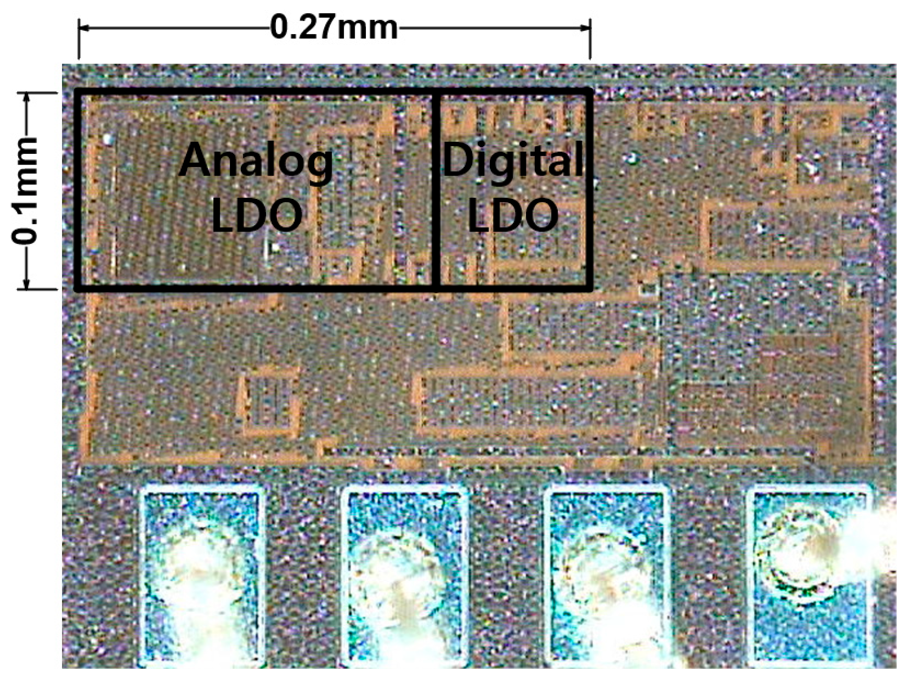
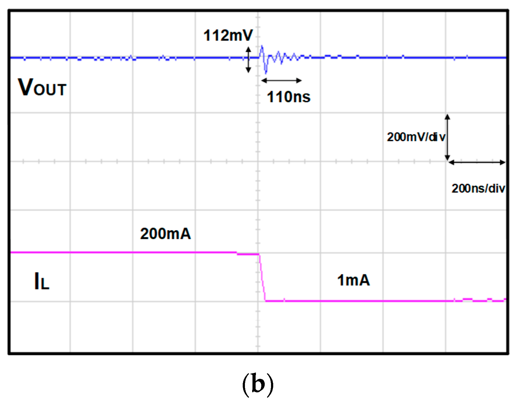
4. Measurement Results

A prototype of the proposed DA-HLDO is verified in a 1.2 V 65 nm CMOS process. The chip micrograph is shown in Figure 12. The active area of the DA-HLDO is 0.027 mm2. The output voltage is 0.9–1.0 V from the input supply of 1.1–1.2 V, and the DA-HLDO can deliver a 200 mA current at maximum while consuming 200 μA quiescent current. The size of the analog power transistor is 200/0.06, and the size of one digital power transistor in the 15-bit array is 25/0.06, all in μm.
The proposed circuit has a minimum of 3 mV/V line regulation when a reference voltage is 900 mV at 200 mA load current and a maximum of 6 mV/V when the reference voltage is 1.1 V, as shown in Figure 13a. The load regulation is also checked at three reference voltages when load variation is from 1 mA to 200 mA. When the reference voltage is 900 mV, the minimum load regulation is 2 mV/mA, and the maximum load regulation is 11 mV/mA at 1.1 V reference voltage, as shown in Figure 13b. In 1.2 V input voltage and 200 mV dropout voltage, Figure 14 shows that the undershoot/overshoot, with the corresponding settling time measured under a load current step of 200 mA/10 ns (CL = 8 nF), are 82 mV/89 ns and 112 mV/110 ns, respectively.
Table 2 presents a performance summary of this work and a comparison with recently published solutions, including digital, analog, and hybrid-mode architectures. The figure of merit (FOM) is 4.48 ps and makes this design competitive among all types of architectures. All LDOs presented in Table 2, with the exception of those reported in references [23,31], can support an output load current exceeding 100 mA. The PSRR results of the proposed DA-HLDO solution proposed in this manuscript are comparable to the best results found in the existing literature, specifically under full load conditions. However, our proposed LDO distinguishes itself with a smaller area and a shorter settling time, resulting in an improved FoM.
In the static mode, where only ALDO works, only the 40 μA quiescent current required by EA is consumed. In the dynamic mode of ALDO and DLDO work, the quiescent current consumed is 200 μA. The quiescent current is smaller than most of the LDOs because the digital controller is disabled in steady state to eliminate switching noises. By powering down the digital part, we can reduce the quiescent current at steady state even when using the flash ADC.

5. Conclusions

This article proposes a self-triggered digitally assisted hybrid LDO that truly inherits the advantages of tight regulation and wide load current range from analog control, and the merits of fast transient speed and area-efficient power transistor utilization from digital control. The potential of the proposed DA-HLDO lies in that the ALDO is made the master, whereas the DLDO is made the slave. The ALDO is precise and continuous and consequently prevails in regulation and noise suppression. Meanwhile, a DLDO prevails in terms of switching so that fast transient speed is attainable with area-efficient, fully turned on/off power transistors. The DLDO consumes no static current by self-triggering the digital loop on large current steps. Results from the DA-HLDO demonstrate a 110 ns settling time and a FoM as low as 4.48 ps.

Author Contributions

Conceptualization, Z.J. and D.B.; methodology, Z.J. and D.B.; validation, Z.J. and D.B.; formal analysis, Z.J. and G.K.; investigation, Z.J. and G.K.; resources, Z.J. and D.B.; data curation, Z.J.; writing—original draft preparation, Z.J.; writing—review and editing, Z.J. All authors have read and agreed to the published version of the manuscript.

Funding

This work was supported by the Institute for Information & Communications Technology Planning & Evaluation (IITP) grant funded by the Korea government (MSIT) (No. 2019-0-00138, Development of Intelligent Radar Platform Technology for Smart Environments), and Chung-Ang University Young Scientist Scholarship in 2020.

Data Availability Statement

Not applicable.

Conflicts of Interest

The authors declare no conflict of interest.

References

  1. MC13892 Data Sheet, (April 2014). NXP Semiconductors. Available online: http://www.nxp.com (accessed on 19 July 2020).
  2. Duong, Q. Multiple-Loop Design Technique for High-Performance Low-Dropout Regulator. IEEE J. Solid-State Circuits 2017, 52, 2533–2549. [Google Scholar]
  3. Hazucha, P.P.; Karnik, T.; Bloechel, B.A.; Parsons, C.; Finan, D.; Borkar, S. Area-efficient linear regulator with ultra-fast load regulation. IEEE J. Solid-State Circuits 2005, 40, 933–940. [Google Scholar]
  4. Milliken, R.J.; Silva-Martinez, J.; Sanchez-Sinencio, E. Full on-chip CMOS low-dropout voltage regulator. IEEE Trans. Circuits Syst. I Reg. Pap. 2007, 54, 1879–1890. [Google Scholar]
  5. Al-Shyoukh, M.; Lee, H.; Perez, R. A transient-enhanced low-quiescent current low-dropout regulator with buffer impedance attenuation. IEEE J. Solid-State Circuits 2007, 42, 1732–1742. [Google Scholar]
  6. Lau, S.K.; Mok, P.K.T.; Leung, K.N. A low-dropout regulator for SoC with Q-reduction. IEEE J. Solid-State Circuits 2007, 42, 658–664. [Google Scholar]
  7. Guo, J.; Leung, K.N. A 6-µ chip-area-efficient output-capacitorless LDO in 90-nm CMOS technology. IEEE J. Solid-State Circuits 2010, 45, 1896–1905. [Google Scholar]
  8. Or, P.Y.; Leung, K.N. An output-capacitorless low-dropout regulator with direct voltage-spike detection. IEEE J. Solid-State Circuits 2010, 45, 458–466. [Google Scholar]
  9. Kim, G.S.; Park, J.K.; Ko, G.H.; Baek, D. Capacitor-Less Low-Dropout (LDO) Regulator with 99.99% Current Efficiency Using Active Feedforward and Reverse Nested Miller Compensations. IEEE Access 2019, 7, 98630–98638. [Google Scholar]
  10. Okuma, Y. 0.5-V input DLDO with 98.7% current efficiency and 2.7-quiescent current in 65 nm CMOS. In Proceedings of the IEEE Custom Integrated Circuits Conference 2010, San Jose, CA, USA, 19–22 September 2010. [Google Scholar]
  11. Lee, Y.H. A low quiescent current asynchronous digital-LDO with PLL-modulated fast-DVS power management in 40 nm SoC for MIPS performance improvement. IEEE J. Solid-State Circuits 2013, 48, 1018–1030. [Google Scholar]
  12. Gangopadhyay, S.; Somasekhar, D.; Tschanz, J.W.; Raychowdhury, A. A 32 nm embedded fully-digital phase-locked low dropout regulator for fine grained power management in digital circuits. IEEE J. Solid-State Circuits 2014, 49, 2684–2693. [Google Scholar]
  13. Nasir, S.B.; Gangopadhyay, S.; Raychowdhury, A. 5.6 A 0.13 μm fully digital low-dropout regulator with adaptive control and reduced dynamic stability for ultra-wide dynamic range. In Proceedings of the 2015 IEEE International Solid-State Circuits Conference—(ISSCC) Digest of Technical Papers, San Francisco, CA, USA, 22–26 February 2015; pp. 98–99. [Google Scholar]
  14. Salem, L.G.; Warchall, J.; Mercier, P.P. 20.3 A 100 nA-to-2 mA successive-approximation digital LDO with PD compensation and sub-LSB duty control achieving a 15.1 ns response time at 0.5 V. In Proceedings of the 2017 IEEE International Solid-State Circuits Conference (ISSCC), San Francisco, CA, USA, 5–9 February 2017; pp. 340–341. [Google Scholar]
  15. Huang, M.; Lu, Y.; Sin, S.W.; Seng-Pan, U.; Martins, R.P. A fully integrated DLDO with coarse-fine-tuning and burst-mode operation. IEEE Trans. Circuits Syst. II Exp. Briefs 2016, 63, 683–687. [Google Scholar]
  16. Yang, F.; Mok, P.K.T. A nanosecond-transient fine-grained DLDO with multi-step switching scheme and asynchronous adaptive pipeline control. IEEE J. Solid-State Circuits 2017, 52, 2463–2474. [Google Scholar]
  17. Lee, Y.J. A 200-mA digital low drop-out regulator with coarse-fine dual loop in mobile application processor. IEEE J. Solid-State Circuits 2017, 52, 64–76. [Google Scholar]
  18. Kim, D.; Seok, M. A fully integrated digital low-dropout regulator based on event-driven explicit time-coding architecture. IEEE J. Solid-State Circuits 2017, 52, 3071–3080. [Google Scholar]
  19. Chen, W.C.; Ping, S.Y.; Huang, T.C.; Lee, Y.H.; Chen, K.H.; Wey, C.L. A switchable digital-analog low-dropout regulator for analog dynamic voltage scaling technique. IEEE J. Solid-State Circuits 2014, 49, 740–750. [Google Scholar]
  20. Nasir, S.B.; Raychowdhury, A. Embedded hybrid LDO topologies for digital load circuits. In Proceedings of the 2016 IEEE Asia Pacific Conference on Circuits and Systems (APCCAS), Jeju, Republic of Korea, 25–28 October 2016; pp. 43–46. [Google Scholar]
  21. Cheah, M.; Mandal, D.; Bakkaloglu, B.; Kiaei, S. A 100-mA 99.11% current efficiency 2-mVpp ripple digitally controlled LDO with active ripple suppression. IEEE Trans. Very Large Scale Integr. Syst. 2017, 25, 696–704. [Google Scholar]
  22. Huang, M.; Lu, Y.; Seng-Pan, U.; Martins, R.P. An analog-assisted tri-loop digital low-dropout regulator. IEEE J. Solid-State Circuits 2018, 53, 20–34. [Google Scholar]
  23. Park, J.E.; Jeong, D.K. A fully integrated 700 mA event-driven digital low-dropout regulator with residue-tracking loop for fine-grained power management unit. In Proceedings of the 2018 IEEE Symposium on VLSI Circuits, Honolulu, HI, USA, 18–22 June 2018; pp. 231–232. [Google Scholar]
  24. Lu, Y.; Yang, F.; Chen, F.; Mok, P.K.T. A 500 mA analog-assisted digital-LDO-based on-chip distributed power delivery grid with cooperative regulation and IR-drop reduction in 65 nm CMOS. In Proceedings of the 2018 IEEE International Solid-State Circuits Conference—(ISSCC), San Francisco, CA, USA, 11–15 February 2018; pp. 310–312. [Google Scholar]
  25. Lu, Y.; Yang, F.; Chen, F.; Mok, P.K.T. A distributed power delivery grid based on analog-assisted DLDOs with cooperative regulation and IR-drop reduction. IEEE Trans. Circuits Syst. I Reg. Pap. 2020, 67, 2859–2871. [Google Scholar]
  26. Liu, X.; Krishnamurthy, H.K.; Na, T.; Weng, S.; Ahmed, K.Z.; Ravichandran, K.; Tschanz, J.; De, V. 14.7 A modular hybrid LDO with fast load-transient response and programmable PSRR in 14 nm CMOS featuring dynamic clamp tuning and time-constant compensation. In Proceedings of the 2019 IEEE International Solid-State Circuits Conference-(ISSCC), San Francisco, CA, USA, 17–21 February 2019; pp. 234–236. [Google Scholar]
  27. Zhou, D.; Jiang, J.; Liu, Q.; Soenen, E.G.; Kinyua, M.; Martinez, J.S. A 245-mA digitally assisted dual-loop low-dropout regulator. IEEE J. Solid-State Circuits 2020, 55, 2140–2150. [Google Scholar]
  28. Jung, J.H.; Hong, S.K.; Kwon, O.K. A fast transient response hybrid LDO with highly accurate DC voltage using countable bidirectional binary search and soft swap switching. IEEE Trans. Circuits Syst. II Exp. Briefs 2020, 67, 3272–3276. [Google Scholar]
  29. Kwok, K.C.; Mok, P.K.T. Pole-zero tracking frequency compensation for low dropout regulator. In Proceedings of the 2002 IEEE International Symposium on Circuits and Systems (ISCAS), Phoenix-Scottsdale, AZ, USA, 26–29 May 2002; p. 4. [Google Scholar]
  30. Briseno-Vidrios, C. A 44-fJ/Conversion step 200-MS/s pipeline ADC employing current-mode MDACs. IEEE J. Solid-State Circuits 2018, 53, 3280–3292. [Google Scholar]
  31. Huang, M. 20.4 An output-capacitor-free analog-assisted digital low-dropout regulator with tri-loop control. In Proceedings of the 2017 IEEE International Solid-State Circuits Conference (ISSCC), San Francisco, CA, USA, 5–9 February 2017; pp. 342–343. [Google Scholar]
  32. Magod, R.; Bakkaloglu, B.; Manandhar, S. A 1.24 μA Quiescent Current NMOS Low Dropout Regulator with Integrated Low Power Oscillator-Driven Charge-Pump and Switched-Capacitor Pole Tracking Compensation. IEEE J. Solid-State Circuits 2018, 53, 2356–2367. [Google Scholar]
  33. Nasir, S.B.; Sen, S.; Raychowdhury, A. Switched-Mode-Control based hybrid LDO for fine-grain power management of digital load circuits. IEEE J. Solid-State Circuits 2018, 53, 569–581. [Google Scholar]
Figure 1. (a) Basic scheme and (b) recent scheme of the SoCs.
Electronics 12 03215 g001
Figure 2. Topology of a conventional (a) ALDO and (b) DLDO.
Electronics 12 03215 g002
Figure 3. Architecture of the proposed DA-HLDO.
Electronics 12 03215 g003
Figure 4. FSM of the digital controller.
Electronics 12 03215 g004
Figure 5. Timing diagram of the proposed DA-H LDO for a load step from 1 mA to 200 mA.
Electronics 12 03215 g005
Figure 6. Simulation results of the PSRR, VIN = 1.2 V, VOUT = 1 V, CL = 8 nF.
Electronics 12 03215 g006
Figure 7. Circuit implementation of the EA.
Electronics 12 03215 g007
Figure 8. Simulated LDO loop response for different load currents.
Electronics 12 03215 g008
Figure 9. Circuit implementation of comparator for the event-driven ADC.
Electronics 12 03215 g009
Figure 10. Circuit implementation of the ring oscillator-based clock generator.
Electronics 12 03215 g010
Figure 11. Circuit implementation of the 4-bit flash ADC.
Electronics 12 03215 g011
Figure 12. Die photograph of the proposed digitally assisted hybrid LDO.
Electronics 12 03215 g012
Figure 13. Measured (a) line regulation and (b) load regulation.
Electronics 12 03215 g013
Figure 14. Measured load transient waveforms responding to (a) 1 mA to 200 mA /10 ns (b) 200 mA to 1 mA/10 ns load current step.
Electronics 12 03215 g014aElectronics 12 03215 g014b
Table 1. Comparison table of analog LDO and digital LDO.
Analog LDODigital LDO
Quantization ErrorNOYes
Dropout VoltageHighLow
Area EfficiencyLowHigh
Settling TimeSlowFast
PSRRGoodPoor
Output RippleNoYes
Table 2. Comparison of the proposed LDO with published state-of-the-art LDOs.
Publication[13][16][24][32][33][27]This Work
ISSCC’15JSSC’18JSSC’17JSSC’18JSSC’18JSSC’20
Process [nm]130651302501304065
ArchitectureDigitalDigitalAnalogAnalogHybridHybridHybrid
Active Area [mm2]0.3550.1580.18250.1080.08180.0560.027
VIN (V)0.5–1.20.6–1.01.05–2.01.5–3.31.1–1.21.25–1.41.1–1.2
VOUT (V)0.45–1.140.55–0.9521.0–3.00.8–1.11.1–1.250.9–1.0
IL, MAX [mA]4.650030015012245200
CL [nF]11.5100010000.5208
IQ [μA]24–22130014-120100163.2300200
ΔVout [mV]
@ΔIL [mA]
<40
@0.7
50
@100
56
@300
160
@150
240
@10
71
@240
112
@200
Ts [us]1.10.0250.252000.0520.520.11
PSR [dB] @ 1 MHz
for Max Load
N/AN/A−12−36N/A−4340
FoM [ps] *>452.312.447.41667.44.48
*   F o M   = C L × Δ V × I Q Δ I m a x 2 .
Disclaimer/Publisher’s Note: The statements, opinions and data contained in all publications are solely those of the individual author(s) and contributor(s) and not of MDPI and/or the editor(s). MDPI and/or the editor(s) disclaim responsibility for any injury to people or property resulting from any ideas, methods, instructions or products referred to in the content.

