Abstract
Modular multiplication is a crucial operation in public-key cryptography systems such as RSA and ECC. In this study, we analyze and improve the iteration steps of the classic Montgomery modular multiplication (MMM) algorithm and propose an interleaved pipeline (IP) structure, which meets the high-performance and low-cost requirements for Internet of Things devices. Compared to the classic pipeline structure, the IP does not require a multiplexing processing element (PE), which helps shorten the data path of intermediate results. We further introduce a disruption in the critical path to complete an iterative step of the MMM algorithm in two clock cycles. Our proposed hardware architecture is implemented on Xilinx Virtex-7 Series FPGA, using DSP48E1, to realize the multiplier. The implemented results show that the modular multiplication of 1024 bits by 2048 bits requires 1.03 s and 2.13 s, respectively. Moreover, our area–time–product analysis reveals a favorable outcome compared to the state-of-the-art designs across a 1024-bit and 2048-bit modulus.
1. Introduction
1.1. Research Background
With the rapid advancement of communication technology, the Internet of Things (IoT) represents a technological revolution that makes future computing and communications different []. IoT devices, ranging from wearable devices and smartphones to wireless sensors, offer a multitude of applications across various fields, including big data, business analytics, and information sharing []. However, the diverse nature of IoT devices and the vast amount of handled sensitive data pose challenges in terms of consumer privacy and secure data transfer []. To address these concerns, the adoption of cryptography solutions is imperative to ensure user authentication and data security. A public-key cryptography system (PCS) plays a fundamental role in information security []. There are various PCS-based communications protocols and sensitive applications (e.g., the transport layer security (TLS) protocol []), which are widely used in Internet communications. Based on TLS and HTTPS protocols, a cloud server is able to authenticate IoT devices. Additionally, in the IoT field, blockchain is a popular public-key cryptography-based technology that prevents IoT devices from attacks and synchronizes them []. However, due to limited resources, IoT devices seek cheap and efficient implementations of PCS. Software implementations can achieve basic PCS functions but suffer from limited memory, battery power, and computing power [,]. Hardware implementations can solve computational burdens and limited memory problems since they perform better and do not occupy the computational resources of a central processor. Some existing works [,,] are dedicated to the efficient hardware implementations of PCS with low areas.
Modern PCSs are represented by Rivest–-Shamir–-Adleman (RSA), proposed in 1978 [], and elliptic curve cryptography (ECC), proposed by Miller [] and Koblitz [] in 1986. ECC-based cryptography systems offer certain advantages over RSA, such as shorter key sizes and faster decryption computation speeds. However, it is essential to note that RSA-based cryptography systems still maintain their significance and find extensive usage in various scenarios. For instance, RSA is widely employed in authentication mechanisms, like the DHE-RSA and ECDHE-RSA algorithms within TLS version 1.3. Despite the emergence of ECC, RSA remains extensively supported in many security applications because it has simpler computational steps compared to ECC.
The computations of point multiplication in ECC and modular exponentiation in RSA both require modular multiplications that significantly occupy most of the encryption and decryption times. Considering the resource limitations of IoT devices, there is a growing need for cost-effective solutions. Consequently, the design of an efficient modular multiplier to accelerate the execution speed has become a crucial requirement. Montgomery modular multiplication (MMM) [] is a widely adopted solution that offers the capability to convert modular operations into binary-shift operations, which makes it an attractive choice for accelerating PCS computations in IoT devices at low costs.
1.2. Previous Work
Efforts have been made to optimize the performance and area utilization of MMM hardware implementations. These works can generally be classified into two main categories.
The first one involves digit-serial implementations based on the high-radix form of MMM. Ref. [] proposed a classic low area-cost architecture with radix-8 MMM. However, this architecture suffers from long carry-chains, resulting in long total latency. To solve this, ref. [] also employed booth encoding and the compression method, but there is still the long critical path delay (CPD) issue. To further improve the performance, some state-of-the-art works made efforts on different optimizations. Ref. [] proposed a fixed-precision MMM to reduce expensive multiplication on computing partial results. Booth encoding and comprehensive scheduling are also involved in improving performance and achieving scalable design. However, much logic designed for encoding and computing intermediate results costs a lot of resources, which is not applicable to IoT devices. Ref. [] made great efforts to improve the parallelism of computing intermediate results based on full adders (FAs) and only used carry–save adders (CSAs) on the final subtraction. Ref. [] employed fast adders, including CSAs, partial full adders, and carry look-ahead adders, to improve performance based on proper scheduling. However, both [,] were limited in balancing performance and resource efficiency. Ref. [] proposed an iterative MMM based on a comprehensive analysis of data dependency, encoding, and compression methods, which contributes to improving performance a lot, but the area cost is also considerably high. Ref. [] used carry–select adders to shorten the total latency. However, it is important to note that high-performance adders typically come with trade-offs, such as increased area costs or a constrained radix, which may limit their flexibility. Ref. [] focused on an optimized redundant binary MMM representation that had the advantage of a small CPD based on the proposed pipeline. The trade-off made by [] involved the extra operation cycles in converting the redundant binary representation to binary representation. Ref. [] proposed architecture using lookup tables (LUTs) to pre-compute the partial results and showed that, in their design, using FA is more area-efficient than using CSA. Their work may need more optimizations on the bottom layer of multiplication to achieve higher performance. Ref. [] introduced a radix-2 design with concise hardware architecture and low area costs, but the total latency was also high.
The second category of works focused on scheduling the operations of MMM using different multiplication algorithms, such as Karatsuba multiplication [] and Toom–Cook multiplication []. Despite their superior performance, area trade-offs need to be considered in [,] because of the added logic implemented in their multiplication algorithms. Additionally, other works improved the performance by focusing on unconventional multiplication systems, like fast Fourier transform (FFT) [], the residue number system (RNS) [,], and the non-least positive (NLP) form []. However, it is worth noting that these multiplication systems require a significant amount of hardware resources, especially when dealing with large input sizes. Regarding [,], their systems have efficient multiplication without carrying propagation, improving the processing speed of MMM itself. Even so, the area cost of conversion between weighted binary numbers and residue numbers is still high and results in low area efficiency overall. This category of work with complex multiplication algorithms or systems is not suitable for IoT devices where the resources are highly restricted.
Even though various works have focused on optimizing the multiplication operations of MMM, there have been fewer inventive modifications made to the iteration steps of the MMM algorithm itself. Among the mentioned works, almost all of them employed the classic pipeline form of MMM introduced in [] in 1999. Although [] proposed a different iterative MMM algorithm based on encoding and compression methods, the basic bit-wise scanning steps have not changed. Several other works attempted to modify the classic MMM pipeline to reduce the total clock cycles or increase the maximum clock frequency. Ref. [] modified the input data paths of each processing element, aiming to enhance the pipeline structure. Ref. [] relaxed the data dependency by reducing the operands, leading to a new pipeline form. Ref. [] introduced a separate iterative MMM that needs pre-computation, making the calculation process more efficient. However, refs. [,,] did not modify the core iteration steps and needed extra resources with the carry–save adders. Ref. [] introduced inventive changes to both the data dependency and the iteration steps of the MMM algorithm. Although this modification aimed to improve the overall performance, it resulted in a considerable increase in the critical path length due to the extended data paths.
Previous research studies have indeed emphasized adder performance optimizations and the use of higher-performing multiplication algorithms. Adder optimizations have involved compression and encoding methods as well as different addition systems, while multiplication algorithm optimizations have primarily focused on scheduling classic iteration steps of MMM. However, in our work, we aim to approach optimization differently. We do not consider optimization methods, such as encoding, data compression, or data preprocessing, as they do not yield significant benefits compared to algorithm optimization. Instead, our motivation lies in optimizing the performance and reducing area costs by modifying the classic iteration steps of the MMM algorithm. We also explore a new pipeline form and comprehensive scheduling that is specifically tailored to hardware implementations.
1.3. Paper Contributions
In this paper, we present a high-performance, low-cost Montgomery modular multiplier based on the proposed interleaved pipeline of MMM. The main contributions of this paper are as follows:
(1) We modify the iteration steps of the classic MMM algorithm and propose the interleaved pipeline multiple-word radix- Montgomery multiplication (-) algorithm. This modification allows us to reduce the data path length of intermediate results by eliminating the necessity of reusing processing elements (PEs). The execution steps of the interleaved pipeline (IP) form are also presented in our work.
(2) To improve the operating frequency, we schedule an iterative step in the - algorithm to execute in two clock cycles. By doing so, the calculation of the coefficient in - algorithm can be completed for one extra cycle of time instead of being completed within one cycle. This can reduce the (CPD) and the overall computation time of MMM.
(3) We provide a comprehensive hardware structure for our proposed algorithm, including the design of each PE and the overall architecture. The implementation utilizes DSP48E1 blocks on the Xilinx Virtex-7 FPGA series. Additionally, we performed a detailed analysis of the performance and area costs, demonstrating that our approach achieves superior performance in terms of area at a lower level.
The remainder of this paper is organized as follows. Section 2 presents the preliminary for radix-2 Montgomery multiplication, high-radix Montgomery multiplication, and the pipeline form of high-radix MMM. Section 3 introduces the proposed - algorithm and its corresponding pipeline form. It also presents the hardware architecture for each PE and the overall system. In Section 4, we analyze the performance and area cost and provide a comparison of state-of-the-art implementations. Finally, we conclude this paper in Section 5.
2. Preliminaries
This section provides an overview of the classic radix-2 Montgomery multiplication () algorithm and classic multiple-word radix- Montgomery multiplication () algorithm, covering their backgrounds and basic notations. This section also analyzes the data dependency and limitations of the classic pipeline of the algorithm when implemented on hardware.
2.1. Radix-2 Montgomery Modular Multiplication Algorithm
The MMM algorithm has two forms based on the different radices of the multiplicand: the form and the form. The form only requires performing an add operation as the multiplicand just needs to determine if the multipliers need to be added to the result. This form is widely used in resource-limited systems due to its simplicity. The form performs actual multiplication because both the multiplicand and multiplier are scanned over multiple bits. Under the requirement of multipliers, the form can reach higher performance than the form but results in more resource utilization. Using DSP blocks on FPGAs is a convenient way to meet the need for multipliers. Algorithm 1 presents the detailed pseudo-code for classic .
| Algorithm 1 Classic radix-2 Montgomery multiplication []. |
|
In Algorithm 1, S is the n-bit result of . Q is a variable to determine if M needs to be added to step 4. Steps 3 and 4 are always performed within a loop and can be implemented on hardware in a pipeline style. Nevertheless, S needs to be compared to M and subtracted if it is greater than M in step 7. Thus, the pipeline must stall if we want to use result S to perform continuously.
2.2. Multiple-Word Radix- Montgomery Modular Multiplication Algorithm
In [], an optimized radix- MMM algorithm is provided without the final quotient determination by simply adding a zero-value word on the most significant bit (MSB) of the multiplicand X. Therefore, the pipeline does not need a stall and can perform MMM continuously just after the results are calculated. Here, we provide a classic algorithm without the final subtraction, as shown in Algorithm 2, based on the algorithm proposed in [].
| Algorithm 2 Classic multiple-word radix- Montgomery multiplication [] |
|
In Algorithm 2, is the negative modular multiplicative inverse of the modulus M and treated as a pre-calculated parameter because it is only determined by M, which is a constant during the calculation of . The initial precision of M is n bits. However, during the computation, both Y and M have words, where an extra zero-value word is added, since the result S needs an extra word to obtain precision extended to the correct value []. According to [], X is also extended with an extra zero-value word to avoid final subtraction. C needs to be considered when it comes to . It represents the carry bits that are propagated from the computation of one word to the next word. represents the jth word of C in ith loop. The concatenation of vectors C and S is represented as . S is calculated after scanning X once and shifting r bits to the right.
2.3. Pipeline of the Classic Algorithm
A classic pipeline form suitable for the multiple-word radix-2 Montgomery multiplication () algorithm was mentioned in []. Based on the pipeline of , the pipeline form under can be obtained with a slight modification, as shown in Figure 1.
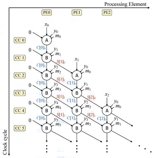
Figure 1.
Classic pipeline of .
For this classic high-radix pipeline (CHRP), a column represents one PE, which is one pipeline stage (PS). A row represents one clock cycle (CC). Each PE has two calculation states, A and B. A state represents the first clock period when the PE starts to calculate. In this cycle, a PE does not require carrying bits C, and at the end of the cycle, the result of PE[i] cannot be obtained immediately. In the B state, PE[i] requires the carry bit to compute at the end of CCs. Here, we note that the result of PE[i] is passed on to the next PE[] and the carry bits are passed to the current PE[i]. According to the natural characteristics of the classic algorithm, the radix size r cannot exceed the word size w. Therefore, the number of PSs in CHRP cannot exceed . Otherwise, more PEs may reduce performances on more CCs. This is concluded from [], where the performance is analyzed thoroughly with different numbers of PSs and word sizes.
Since the number of PSs is limited, the upper limit of the processing speed of CHRP design depends on the word size w and the performance of multipliers. Moreover, under CHRP, reusing PEs is necessary to achieve high parallelism and improve computation efficiency. However, the requirement for reusing PEs introduces the challenge of passing the intermediate result S from the last PE to the first PE. This can lead to a high net delay when implemented on hardware, potentially impacting the overall performance. One possible approach to mitigate the net delay is to use buffers on the result S within the pipeline. By inserting buffers, the net delay can be reduced, but this comes at the cost of additional CCs and increased complexity in managing the flow of data. Finding the right balance between parallelism (in CCs) and frequency (in net delay) is indeed a trade-off that needs to be considered. It requires careful optimization techniques to achieve the desired performance while taking into account the available resources and other limitations.
3. Proposed Interleaved Pipeline Design
In this section, we introduce the proposed - algorithm, which aims to improve the performance and efficiency of the classic algorithm by modifying the iteration steps. Based on the - algorithm, we present a novel pipeline form, IP. This pipeline form takes advantage of the modified iteration steps and data dependency to achieve better performance, since the long data path of reusing PEs is avoided. Notably, we introduce an interruption in the critical path, which involves adding a pipeline stage within a PE to compute the intermediate result S. This approach allows for a higher operating frequency and faster computation. Furthermore, we present the hardware architecture of PEs and the overall design of the MMM multiplier based on the - algorithm.
3.1. Proposed IP-MWRMM Algorithm
To modify the iteration steps of the classic algorithm, we reverse the data path of and at PE[i] and propose a novel - algorithm, as shown in Algorithm 3.
The initial precision of M is n bits. Multiplicand X is extended with extra zero-value words to omit the final reduction of S. Different from classic , the number of zero-value words added to the MSB of Y and M depends on the parity of to ensure g is even. Thus, we can always calculate S twice with two adjacent words when scanning X, which contributes to simplifying the architecture of the pipeline. The lower bits of a w-bit word are represented as and the higher r bits of a w-bit word are represented as . S is shifted on steps 20 to 26 and concatenated to the correct position with the help of checking the value of t. To understand Algorithm 3, we provide an execution example, as shown in Figure 2, where , , and .
| Algorithm 3 Proposed interleaved pipeline . |
|
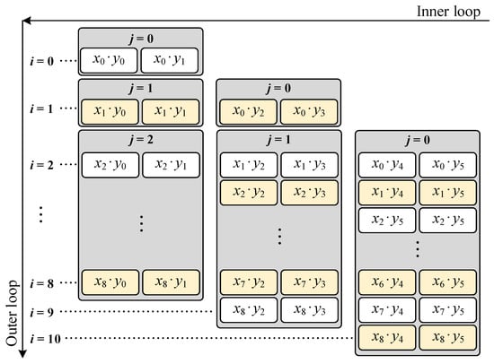
Figure 2.
Execution steps of - (, , and ).
In Figure 2, we provide a high-level overview of the pipeline structure based on the - algorithm, where steps 17 and 18 are key computation steps represented by the multiplication of and . The data dependency and results of every step are discussed in the following subsection. X and Y are divided and expanded to words and words, respectively. The upper bound of the inner loop is 0 (when i is 0), 1 (when i is 1 or 9), or 2 (when i is from 2 to 8), and is determined by steps 8 to 14 in Algorithm 3. Within an inner loop, S is computed twice with two neighboring words of Y. The core difference of the - algorithm is that the scanning steps of X are reversed. X is only scanned between different inner loops while the classic algorithm performs it in the outer loop.
3.2. Parallel Computation of the IP-MWRMM Algorithm
In this subsection, the proposed IP form is presented, along with an analysis of the data dependency and computation efficiency. Figure 3 provides an illustration of the IP structure.
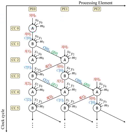
Figure 3.
Proposed pipeline of -.
In Figure 3, each column represents a PE, which can be seen as a PS. The computation of the inner loop, where in Algorithm 3, is represented in CC0 and CC1, and only PE[0] is active. When , the computation of the inner loop is represented in CC2 and CC3, where both PE[0] and PE[1] are active. Figure 3 also shows the detailed data dependency and the transmission direction of the carry bits (C) and results (S) through the PEs. There are two states of PE: A and B. When PE[i] is in the A state, it receives the carry bits C passed from the previous PE[], as well as the result S from itself. For the B state, PE[i] needs the result S transferred from the next PE[] and the carry bits C from itself. Thus, the data dependency changes in every CC, resulting in the interleaved pipeline architecture. The coefficient Q that is multiplied by M is computed on the fly, which means that PE[0] is also responsible for calculating Q when in the A state.
Because of the data dependency of S, the architecture of IP is non-scalable and the total number of PEs requires the following:
Since a PE scans two neighboring words of Y and needs two CCs to scan an X word, the total computation time (measured in CCs) is as follows:
Reviewing the CHRP and we can find its maximum total number of PEs is as follows:
Under this condition, the total computation time (measured in CCs) is as follows:
Comparing the total number of PEs with the computation times of CHRP and IP, we find that the computation efficiency is the same in terms of the CCs and resources. However, the reachable maximum frequencies of two pipeline forms are different because of the data dependency of S. In our proposed IP form, the reuse of PEs is not a must, and the results S are only passed between two neighbor PEs, while PEs must be reused in CHRP, resulting in a long path of S being passed from the last PE to the first one. Another improvement of IP is that when continuously performing MMMs, the final result can be passed directly to the neighbor PEs to perform the next computation. In CHRP, PE[0] must wait to be idle if is not equal to .
To improve the operating frequency, we break one CC into two to allow for separate computations of and . This modification results in one state of the PE that occupies two CCs instead of the original interleaved design shown in Figure 3. Hence, benefits taken by this modification involve reducing the lengths of the carry chains when computing the result S and, therefore, improving the overall computational speed of the MMM.
3.3. Proposed Hardware Architecture
3.3.1. Processing Elements
PE[0] is different from other PEs as it needs to perform the computation of Q on the fly, as shown in Figure 4, where the multipliers are implemented with DSPs on the Xilinx Virtex-7 FPGA series.
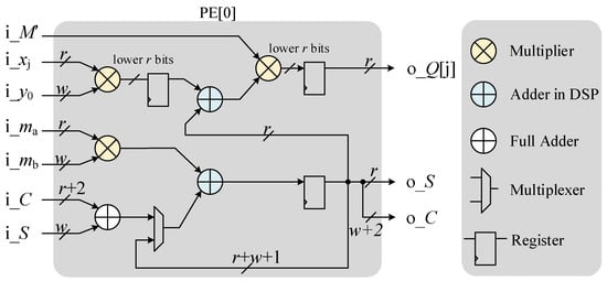
Figure 4.
Hardware architecture of PE[0].
An inner loop in Algorithm 3 is performed in four CCs instead of the original two CCs within a PE because of the modification we made to compute and separately. Situations of inputs i and i are shown in the following equations:
The computation result is , which represents the updated values of . In the modified pipeline design, PE[0] starts computing 5 CCs earlier than PE[1]. By adding an extra CC, we can compute earlier because needs two CCs to output while the result only needs one CC. For an example, is calculated at CC0 and is calculated at CC1. At CC2, is already computed and is calculated, which is . At CC3, is calculated. is computed at CC4, and then PE[1] will be activated at CC5.
The other PEs have the same hardware architecture, but are simpler with only a DSP, a full adder, a 2–1 multiplexer, and a register, as shown in Figure 5. These PEs all require four CCs to compute a step within the inner loop in Algorithm 3.
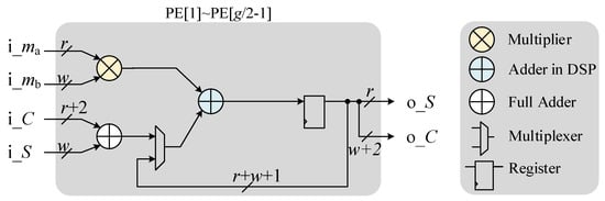
Figure 5.
Hardware architecture of PE[1] to PE[].
3.3.2. Overall Architecture
Figure 6 depicts the overall architecture, where X, Y, and M are sequentially inputted into shifting registers. The computation of Q is performed by PE[0] and subsequently fed into another shifting register. We can recognize that the data only pass between neighbor PEs and the last PE is not responsible for passing the result S to the first PE. Consequently, the net delay is reduced, and the need for additional buffers to store S is eliminated. Furthermore, the last PE needs an additional register to store S for one CC because C and S are generated simultaneously but used in different CCs. The proposed architecture requires more multiplexers compared to CHRP due to the PEs performing different computations in different CCs. With the help of the concise architecture of PEs, all we need to control is the select port of the multiplexers and the shift of registers, which are only determined by PE states.
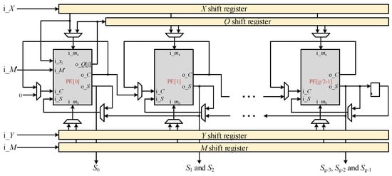
Figure 6.
Overall architecture.
4. Implementation Results and Comparison
In this section, we conduct a comprehensive analysis of the timing, critical path, and area costs of our proposed design. We present the implementation results for the 1024-bit and 2048-bit modulus scenarios. Furthermore, we compare our design with existing works to demonstrate its exceptional performance and superiority.
4.1. Performance and Area Analysis
4.1.1. Timing Analysis
In Figure 3, we separate one CC into two to implement a deep pipeline; thus, the total computation time (measured in CCs) is as follows:
Despite the increase in total CCs, the original CPD of the proposed IP is reduced due to the reduction of the long addition chain in from three additions to two. Moreover, the input bit width of the DSP48E1 module is 18 × 25 with a sign bit. Since our design exclusively uses unsigned numbers, the effective bit width of the inputs is 17 × 24.
The critical path of our hardware architecture depends on the radix r and word size w. When the bit width of r is lower than 17 and w is lower than 24, the critical path is between the output of and the output of . Optimizing this critical path is challenging since it involves addition followed by multiplication. However, if r is still below 17 but w is beyond 24, more than one DSP block should be employed to ensure the multiplication of computed within a single CC. In this case, the critical path arises in the path of multiplication followed by the addition for i_ and i_, with the carry bit being propagated from one DSP to another. Nevertheless, the net delay in the computation of remains unaffected as it only requires the lower r bits of ; the number of DSP blocks required is one.
Furthermore, there is a great need to perform MMM operations continuously in PCSs such as RSA and ECC. In this scenario, the average computation time for a single MMM operation is reduced due to the uninterrupted execution of the pipeline. Given the times () that MMM need to perform, the average computation time (in CCs) of one MMM is shown as (7).
where is near when , revealing that the more the MMM performs, the fewer the total CCs. We adopt as the evaluation of the clock cycles required to perform one MMM operation in our implementation, because our IP form has the property of calculating MMM continuously without any stall between every MMM operation. So, represents the actual performance when our design is used in applications like point multiplication in ECC and modular exponentiation in RSA.
4.1.2. Area Analysis
The area of the proposed architecture can be evaluated by considering the number of PEs, as shown in Equation (1). However, it is important to note that the resource requirements within a single PE vary depending on the size of the radix r and the word size w. Specifically, within a PE, the number () representing the implemented DSPs can be calculated as follows:
Equation (8) shows the trade-offs that can be made in the area of DSPs and the performance. The higher the radix is, the more computations are made within a CC, and the total CC is reduced. However, the number of DSPs is increased at the same time. When the radix and the word size , as well as the multiplication of i_ by i_, can be implemented using a single DSP. In this case, the total number of DSPs required is , which is equal to the number of . It is also possible to cascade DSPs when as long as r is less than or equal to 24. However, an important point to consider is that the computational efficiency is reduced when r exceeds 24, because , and it would require cascading multiple DSPs and adding the results of the DSPs to obtain the correct value. Therefore, we can conclude from Equation (8) that when implementing designs with DSPs, the condition radix and the word size have the smallest DSP area. We implement and in our design to cut down the area.
The resource usage of a full adder is evaluated based on the number of LUTs it occupies. A one-bit full adder has three inputs and two outputs, corresponding to two LUT3 resources in an FPGA, equivalently, one LUT6 resource. The total number of LUT resources occupied by the full adders, denoted as , can be calculated in the following two cases:
4.2. Results Comparison and Discussion
In the proposed hardware implementation of MMM, we used a radix r of 16 and a word size w of 24. The design was implemented using Vivado 2022 on the Xilinx Virtex-7 FPGA Series, with part number XC7V585TFFG1157-3. To provide a comprehensive evaluation, we present the implementation results of four different modulus sizes: 256 bits, 512 bits, 1024 bits, and 2048 bits. These results are compared with other existing works in Table 1.

Table 1.
Comparison of existing works implemented on FPGA.
In Table 1, the Cycles index represents the number of total execution clock cycles, and Period denotes the clock period in nanoseconds (ns). The implementation performance is measured by multiplying Cycles and Period, which is represented by the latency in microseconds (s). The evaluation of the total area takes into account three resource types: SLICEs, DSPs, and BRAMs. To provide a unified standard for expressing the total area, we used the SLICE equivalent cost (SEC) concept [], which is represented by the Total index in Table 1, marked by two asterisks. The SEC value represents the equivalent costs of utilizing different types of resources and allows for a reasonable comparison of the total area requirements between different works. The calculation of SEC is shown as Equation (10).
where represents the number of BRAMs, represents the number of DSPs, and denotes the number of SLICEs. However, in some works, only the LUT and FF numbers are provided. To convert the LUT and FF numbers to an approximate number of SLICEs, we need to consider the architecture of the Xilinx Virtex-6 Series or Virtex-7 FPGA Series. A SLICE in the FPGAs consists of four LUTs, but it is important to note that SLICEs may not be fully occupied in practical designs. Therefore, we use a coefficient of 3.5 as a divisor to estimate the number of SLICEs from the number of LUTs. The formula for calculating the number of SLICEs is as follows:
where #LUT is the number of LUTs. The number under the index SLICE is marked with an asterisk if it is measured by #LUTs, otherwise, it is the actual SLICE number provided in the work.
In order to evaluate the trade-offs between the performance and area in a fair manner and compare the different works, we utilize the area–time–product (ATP) metric:
The ATP is calculated by multiplying the total processing latency by the total area (in SEC). By comparing the ATP values of different works, we can assess the overall efficiency and effectiveness of each design in terms of both performance and area utilization. In addition, the comprehensive comparisons are shown in Figure 7.
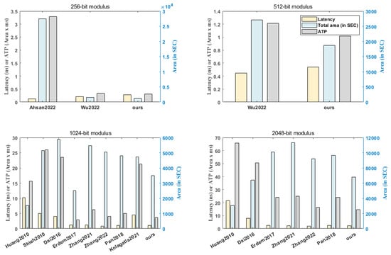
Figure 7.
Comparisons of existing works on FPGA [,,,,,,,,,].
Ref. [] employed the residue number system in their design, achieving lower total latency than ours, outperforming by 56%. However, their work utilized many DSP and SLICE areas because of the extra logic area taken by their system, resulting in low area efficiency. Our implementation improved by 85% in area and 90% in ATP. The area will explode as the bit-width of the modulus increases, so their design is not suitable for a system like RSA, which has a large modulus size. Ref. [] outperforms ours by 21% in latency, but we have an advantage of 26% in area and 6% in ATP for a 256-bit modulus. The advantage of our ATP grows as the modulus size increases. We have an advantage of 16% in ATP for a 512-bit modulus. By this comparison, we can see that our computation efficiency exists even for large modulus sizes.
Although the platform used in [] may be considered outdated, it is still valuable for comparison purposes due to its adoption of a new pipeline form. The architecture in [] shares a similar approach to ours in regard to passing intermediate results, but it suffers from a long data dependency path, resulting in a significant increase in the number of CCs required for computations. Despite the differences in platform frequencies, our work has demonstrated a significant advantage in terms of the number of CCs, achieving a 76% improvement compared to []. Ref. [] aimed to relax data dependencies through reduced operands and proposed a new pipeline form. However, their implementation still exhibited a high total area (in SEC) and total latency, indicating that their approach to the new pipeline design was ineffective. Compared to [], our design significantly improves the ATP by 86%.
The design presented in [] is based on FFT and requires a significant amount of BRAM resources. While FPGAs often have sufficient BRAM resources to accommodate this overhead, the ATP of [] is relatively inferior when considering SEC. Although our design may have an advantage in terms of the platform, it is important to note our absolute leading positions in both total latency and SEC. Latency is improved by 74% in the 1024-bit modulus and by 73% in the 2048-bit modulus. In terms of SEC, our design achieves a 40% improvement in the 1024-bit modulus configuration, while maintaining a slightly higher SEC (by 5% in the 2048-bit modulus design) compared to [].
The designs in [,] are all based on digit-serial MMM and utilize optimized adders or encoding methods to complete the designs. Among them, ref. [] stands out as a competitive design, with a smaller ATP and total SEC compared to ours. However, we maintain an advantage in terms of total latency. It is worth noting that the superior performance in [] under the 1024-bit modulus cannot be well inherited into the design of the 2048-bit modulus. In the case of the 2048-bit modulus, we achieve a 10% advantage in total latency, a 32% advantage in total SEC, and a 40% advantage in ATP over []. Compared to [], we have advantages in total latency, SEC, and ATP. Specifically, for the 1024-bit modulus, we achieve an 8% advantage in total latency, a 35% advantage in SEC, and a 41% advantage in ATP. For the 2048-bit modulus, we have similar total latency, but a 41% advantage in ATP. In [], the design excels in total latency for both the 1024-bit modulus and 2048-bit modulus. However, our design takes the lead in ATP for both modulus sizes. Furthermore, as the modulus size increases, our design maintains its advantage in terms of SEC and ATP. For [], our design has a similar total latency but a 25% advantage in area for the 1024-bit modulus. For the 2048-bit modulus, our implementation outperforms 14% in latency, 29% in area, and 39% in ATP. Compared to [], we have an absolute advantage in both latency and area, represented by an 83% advantage in ATP.
Indeed, comparing and selecting the best design for MMM can be challenging due to the diverse structures and optimizations employed by the listed designs. Each design incorporates different techniques, such as compression, encoding, modified pipelines, as well as different multiplication algorithms. Given the available data, our design stands out with the best ATP and low latency in the 2048-bit modulus scenario. Additionally, it demonstrates our competitive performance in the 1024-bit modulus scenario. Generally, our design shows notable strengths in terms of ATP and latency, making it a compelling choice for Montgomery modular multiplication.
5. Conclusions
This paper proposes a high-performance and low-cost implementation of Montgomery modular multiplication. The proposed interleaved pipeline form of effectively addresses the issue of long data dependency paths, thereby reducing delay. To further enhance the clock frequency, we divided the iteration process in the MMM algorithm into two CCs, effectively shortening the critical path and overall delay. As a result, the proposed MMM algorithm can achieve an average completion time of CCs. The multiplier in our hardware architecture is implemented using DSP48E1 blocks in the Xilinx Virtex-7 FPGA Series. The processing elements in our design feature a simple control structure, which enhances the ease of operation. The implementation results highlight the superior ATP and overall performance of our proposed algorithm and pipeline form. This makes it an attractive solution for IoT devices requiring high performance at a low cost. Moving forward, our future work will aim to further improve performance and area efficiency by leveraging digit-serial MMM and exploring additional optimizations with our proposed IP. Since there are various IoT applications, the IoT chip architectures vary, both in size and power consumption. Therefore, we may optimize the DSP logic into compatible fast-adder logic to be more portable and flexible for different applications.
Author Contributions
Conceptualization, methodology, and writing—original draft preparation, H.L.; software and writing—review and editing, H.L. and S.R.; data curation and validation, H.L., S.R. and J.Z.; visualization and project administration, H.L., X.W. and W.W.; supervision and investigation, S.R. All authors have read and agreed to the published version of the manuscript.
Funding
This work was supported in part by the Chongqing Natural Science Foundation under grant cstc2021jcyj-msxmX1096.
Institutional Review Board Statement
Not applicable.
Informed Consent Statement
Not applicable.
Data Availability Statement
All data can be provided upon reasonable request to the corresponding author.
Conflicts of Interest
The authors declare no conflict of interest.
Abbreviations
The following abbreviations are used in this manuscript:
| IoT | Internet of Things |
| PCS | public-key cryptography system |
| TLS | transport layer security |
| RSA | Rivest–-Shamir–-Adleman |
| ECC | elliptic curve cryptography |
| MMM | Montgomery modular multiplication |
| LUT | lookup table |
| FFT | fast Fourier transform |
| RNS | residue number system |
| NLP | non-least positive |
| - | interleaved pipeline multiple-word radix- Montgomery multiplication |
| PE | processing element |
| CPD | critical path delay |
| radix-2 Montgomery multiplication | |
| multiple-word radix- Montgomery multiplication | |
| MSB | most significant bit |
| multiple-word radix-2 Montgomery multiplication | |
| CHRP | classic high-radix pipeline |
| PS | pipeline stage |
| CC | clock cycle |
| FSM | finite state machine |
| FA | full adder |
| CSA | carry–save adder |
| IP | interleaved pipeline |
| SEC | SLICE equivalent cost |
| ATP | area–time–product |
References
- Madakam, S.; Lake, V.; Lake, V.; Lake, V. Internet of Things (IoT): A literature review. J. Comput. Commun. 2015, 3, 56616. [Google Scholar] [CrossRef]
- Lee, I.; Lee, K. The Internet of Things (IoT): Applications, investments, and challenges for enterprises. Bus. Horizons 2015, 58, 431–440. [Google Scholar] [CrossRef]
- Hassan, W.H. Current research on Internet of Things (IoT) security: A survey. Comput. Netw. 2019, 148, 283–294. [Google Scholar]
- Koblitz, N.; Menezes, A.J. A survey of public-key cryptosystems. SIAM Rev. 2004, 46, 599–634. [Google Scholar] [CrossRef]
- Rescorla, E. SSL and TLS: Designing and Building Secure Systems; Addison-Wesley Reading: Boston, MA, USA, 2001; Volume 1. [Google Scholar]
- Huh, S.; Cho, S.; Kim, S. Managing IoT devices using blockchain platform. In Proceedings of the 2017 19th International Conference on Advanced Communication Technology (ICACT), Pyeongchang, Republic of Korea, 19–22 February 2017; pp. 464–467. [Google Scholar] [CrossRef]
- Imteaj, A.; Thakker, U.; Wang, S.; Li, J.; Amini, M.H. A Survey on Federated Learning for Resource-Constrained IoT Devices. IEEE Internet Things J. 2022, 9, 1–24. [Google Scholar] [CrossRef]
- Thakor, V.A.; Razzaque, M.A.; Khandaker, M.R.A. Lightweight Cryptography Algorithms for Resource-Constrained IoT Devices: A Review, Comparison and Research Opportunities. IEEE Access 2021, 9, 28177–28193. [Google Scholar] [CrossRef]
- Wu, R.; Xu, M.; Yang, Y.; Tian, G.; Yu, P.; Zhao, Y.; Lian, B.; Ma, L. Efficient High-Radix GF (p) Montgomery Modular Multiplication Via Deep Use Of Multipliers. IEEE Trans. Circuits Syst. II Express Briefs 2022, 69, 5099–5103. [Google Scholar] [CrossRef]
- Pan, J.S.; Song, P.; Yang, C.S. Efficient digit-serial modular multiplication algorithm on FPGA. IET Circuits Devices Syst. 2018, 12, 662–668. [Google Scholar] [CrossRef]
- Ding, J.; Li, S. A low-latency and low-cost Montgomery modular multiplier based on NLP multiplication. IEEE Trans. Circuits Syst. II Express Briefs 2019, 67, 1319–1323. [Google Scholar] [CrossRef]
- Rivest, R.L.; Shamir, A.; Adleman, L. A method for obtaining digital signatures and public-key cryptosystems. Commun. ACM 1978, 21, 120–126. [Google Scholar] [CrossRef]
- Miller, V.S. Use of Elliptic Curves in Cryptography; Springer: Berlin/Heidelberg, Germany, 1986. [Google Scholar]
- Koblitz, N. Elliptic curve cryptosystems. Math. Comput. 1987, 48, 203–209. [Google Scholar] [CrossRef]
- Montgomery, P.L. Modular multiplication without trial division. Math. Comput. 1985, 44, 519–521. [Google Scholar] [CrossRef]
- Tenca, A.F.; Todorov, G.; Koç, C.K. High-radix design of a scalable modular multiplier. In Proceedings of the Cryptographic Hardware and Embedded Systems—CHES 2001: Third International Workshop, Paris, France, 14–16 May 2001; Proceedings 3. pp. 185–201. [Google Scholar]
- Zhang, B.; Cheng, Z.; Pedram, M. High-radix design of a scalable montgomery modular multiplier with low latency. IEEE Trans. Comput. 2021, 71, 436–449. [Google Scholar] [CrossRef]
- Erdem, S.S.; Yanık, T.; Çelebi, A. A general digit-serial architecture for Montgomery modular multiplication. IEEE Trans. Very Large Scale Integr. (VLSI) Syst. 2017, 25, 1658–1668. [Google Scholar] [CrossRef]
- Zhang, B.; Cheng, Z.; Pedram, M. An Iterative Montgomery Modular Multiplication Algorithm With Low Area-Time Product. IEEE Trans. Comput. 2022, 72, 236–249. [Google Scholar] [CrossRef]
- Fatemi, S.; Zare, M.; Khavari, A.F.; Maymandi-Nejad, M. Efficient implementation of digit-serial Montgomery modular multiplier architecture. IET Circuits Devices Syst. 2019, 13, 942–949. [Google Scholar] [CrossRef]
- Zhang, Z.; Zhang, P. A Scalable Montgomery Modular Multiplication Architecture with Low Area-Time Product Based on Redundant Binary Representation. Electronics 2022, 11, 3712. [Google Scholar] [CrossRef]
- Kolagatla, V.R.; Desalphine, V.; Selvakumar, D. Area-time scalable high radix Montgomery modular multiplier for large modulus. In Proceedings of the 2021 25th International Symposium on VLSI Design and Test (VDAT), Surat, India, 16–18 September 2021; pp. 1–4. [Google Scholar]
- Abd-Elkader, A.A.; Rashdan, M.; Hasaneen, E.S.A.; Hamed, H.F. Efficient implementation of Montgomery modular multiplier on FPGA. Comput. Electr. Eng. 2022, 97, 107585. [Google Scholar] [CrossRef]
- Gu, Z.; Li, S. A division-free Toom–Cook multiplication-based Montgomery modular multiplication. IEEE Trans. Circuits Syst. II Express Briefs 2018, 66, 1401–1405. [Google Scholar] [CrossRef]
- Dai, W.; Chen, D.D.; Cheung, R.C.; Koc, C.K. Area-time efficient architecture of FFT-based montgomery multiplication. IEEE Trans. Comput. 2016, 66, 375–388. [Google Scholar] [CrossRef]
- Mo, Y.; Li, S. Design of an 8192-bit RNS montgomery multiplier. In Proceedings of the 2017 International Conference on Electron Devices and Solid-State Circuits (EDSSC), Hsinchu, Taiwan, 18–20 October 2017; pp. 1–2. [Google Scholar]
- Ahsan, J.; Esmaeildoust, M.; Kaabi, A.; Zarei, V. Efficient FPGA implementation of RNS Montgomery multiplication using balanced RNS bases. Integration 2022, 84, 72–83. [Google Scholar] [CrossRef]
- Tenca, A.F.; Koç, C.K. A scalable architecture for Montgomery multiplication. In Proceedings of the CHES, Worcester, MA, USA, 12–13 August 1999; Volume 99, pp. 94–108. [Google Scholar]
- Ibrahim, A.; Gebali, F.; Elsimary, H. New and improved word-based unified and scalable architecture for radix 2 Montgomery modular multiplication algorithm. In Proceedings of the 2013 IEEE Pacific Rim Conference on Communications, Computers and Signal Processing (PACRIM), Victoria, BC, Canada, 27–29 August 2013; pp. 153–158. [Google Scholar]
- Shieh, M.D.; Lin, W.C. Word-based Montgomery modular multiplication algorithm for low-latency scalable architectures. IEEE Trans. Comput. 2010, 59, 1145–1151. [Google Scholar] [CrossRef]
- Huang, M.; Gaj, K.; El-Ghazawi, T. New hardware architectures for Montgomery modular multiplication algorithm. IEEE Trans. Comput. 2010, 60, 923–936. [Google Scholar] [CrossRef]
- Orup, H. Simplifying quotient determination in high-radix modular multiplication. In Proceedings of the 12th Symposium on Computer Arithmetic, Bath, UK, 19–21 July 1995; pp. 193–199. [Google Scholar]
- Farzam, M.H.; Bayat-Sarmadi, S.; Mosanaei-Boorani, H.; Alivand, A. Hardware architecture for supersingular isogeny Diffie-Hellman and key encapsulation using a fast montgomery multiplier. IEEE Trans. Circuits Syst. I Regul. Pap. 2021, 68, 2042–2050. [Google Scholar] [CrossRef]
Disclaimer/Publisher’s Note: The statements, opinions and data contained in all publications are solely those of the individual author(s) and contributor(s) and not of MDPI and/or the editor(s). MDPI and/or the editor(s) disclaim responsibility for any injury to people or property resulting from any ideas, methods, instructions or products referred to in the content. |
© 2023 by the authors. Licensee MDPI, Basel, Switzerland. This article is an open access article distributed under the terms and conditions of the Creative Commons Attribution (CC BY) license (https://creativecommons.org/licenses/by/4.0/).