Article

An Input Up to 100-V High Voltage LDO Based a Novel Pre-Regulation and a Simple Clamp Current Circuit

1
School of Electronic Engineering, Xidian University, Xi’an 710071, China
2
Shenzhen Changyuntong Semiconductor Co., Ltd., Shenzhen 518133, China
*
Author to whom correspondence should be addressed.
Electronics 2023, 12(15), 3257; https://doi.org/10.3390/electronics12153257
Submission received: 20 June 2023 / Revised: 19 July 2023 / Accepted: 26 July 2023 / Published: 28 July 2023

Abstract

:
With the aim of improving the small input voltage range and complex structure of the current-limiting circuit in the traditional LDO, a wide-range high-voltage input LDO was designed, which uses a pre-regulation principle and a diode current-limiting protection scheme. Based on the DB HiTek 0.18 μm BCD process model for circuit simulation, the simulation results showed that this proposed LDO can stably output 7.6 V under the input voltage range from 13 V to 100 V. In addition, the load regulation rate was 0.0256 mV/mA, and the line regulation rate was 0.035 mV/V. When the load current exceeded 30 mA, the output voltage was prohibited and overcurrent protection was performed. The measurement results showed that the maximum input voltage of the designed chip could reach 140 V. When the load current exceeded 19 mA, the LDO had no output voltage, which indicates that the current limiting circuit can work stably. The circuit designed in this paper has a simple structure but good stability. To date, the LDO has been applied to other DC-DC power supply chips.

1. Introduction

The LDO (low dropout) regulator is the core of a power management chip, which converts the input voltage into a stable output voltage. For their simple structure and the low line and load regulation, LDOs have been widely used in power supply voltage electronic products with high precision requirements.
With the increasing applications of power management chips, the input power supply voltage is also getting higher, some even reaching 100 V, which is a challenge for the internal LDO module design. For most linear regulators with a typical input voltage range, they will collapse when the input voltage is higher than 5 V, which seriously limits their application in some power management chips with wide input voltage range. The LDO circuit applied to the DC-DC converter with wide input voltage range must be able to withstand the external input high voltage and supply power for the on-chip analog, logic, and drive modules. Therefore, it is necessary to research an LDO with a wide range high voltage input.
A pre-regulator circuit as one method to deal with the above problem has been used in some previous works. The pre-regulator circuit in [1], as shown in Figure 1, has an input voltage of 3.9–20 V. The structure is relatively complicated including two differential input pairs of NMOS and PMOS, a push-pull output stage, a start-up circuit and a resistor network. Although the power consumption of specific values is not mentioned, generally speaking, the more the branch circuits, the greater the power consumption.
The structure of the pre-regulator circuit in [2] is similar to that in [1] and is also composed of two-stage circuits. The first stage uses p-type DMOS to realize the pre-regulator, and the second stage uses an NPN power transistor to obtain a large load current. The pre-regulation module of the circuit in [3] includes a bandgap reference voltage source, a simple error amplifier, a gain stage and an output control unit (source follower). Since the bandgap reference voltage source is adopted, the pre-regulator circuit does not have a large drift with the change in temperature. The pre-regulator circuit mentioned above can convert the higher power supply voltage to the lower voltage to supply power for the LDO and other functional modules. Therefore, it is very important to design a pre-regulator circuit with reliable performance.
Furthermore, the difference between input and output voltage becomes larger, and the power transistor is prone to avalanche breakdown when the LDO operates under a large load current, resulting in the chip being unable to work normally. In order to protect the chip from high temperatures, and the damage caused by overload, it is necessary to design a current-limiting circuit to guarantee it works stably within a certain load current range.
A current-limiting circuit is an essential part of the LDO design. The authors of [4] discuss the working principles, advantages and disadvantages of several commonly used current-limiting technologies when designing an LDO. In general, there are three commonly used current-limiting technologies for the design circuit of an LDO, which have been discussed in [5], as shown in Figure 2. The current-limiting function is realized by connecting the current detection resistor RSNS and the current detection transistor MSNS in series. The stability and accuracy of the current-limiting circuit are good, but layout matching of the current detecting resistor is highly required.
The current limiter in [6] includes three stages; the first stage is a current detection transistor, the second stage is a comparator with an offset voltage, and the third stage is a current-limiting transistor controlled by the comparator. When the detected voltage is above the offset voltage, the output voltage is controlled; The principle of overcurrent protection in [7] is that the output current is detected by a PMOS connected in series with the power transistor. The output voltage is generated by the current through the resistor and compared with the error amplifier. The comparison voltage controls the gate of the power transistor to realize the function of overcurrent detection. The research of [8,9] also describes the output load of LDO, but does not give the detailed design principle. The research of [10,11] mainly studies the stability of the device to ensure that the device will not be damaged when the output is overloaded, and no actual current limit for the circuit is given.
When designing an LDO circuit with high input voltage, the pre-regulator is usually used. The high-power supply input voltage generates a lower voltage through the pre-regulator circuit and which is the power supply for other modules. This not only makes the range of the input power supply larger, but also avoids damage to most devices in the circuit. The design idea of the pre-regulator circuit in this paper is to take the reverse breakdown voltage of the diode as a relatively accurate voltage, and use the high-voltage resistance voltage division principle to generate a suitable output voltage.
To address the disadvantages of the traditional LDO with a small input voltage range and complex current-limiting circuit structure, this paper designs an LDO circuit that works normally in a wide range of high voltage inputs (13–100 V, which may even exceed 100 V), and proposes a current-limiting circuit consisting of a diode. The LDO is simulated by using the DB HiTek 0.18 μm BCD process. Compared with the traditional current-limiting circuit, the current-limiting circuit designed in this paper has a simple structure, greatly reducing the area of the LDO and the cost of the chip. It has been used in some PWM controller modules with DC-DC power supply.
The following sections will provide the details of the designed pre-regulator circuit and current-limiting protection circuit. Section 2 describes the principle of the designed error amplifier and its current-limiting circuit. Section 3 discusses the simulation and measurement results and analysis. Finally, the Conclusion is given in Section 4.

2. Designed High Voltage LDO Structure

The overall structure of the LDO designed in this paper is shown in Figure 3, which is similar to the structure of the traditional LDO, and is composed of a pre-regulator circuit, an error amplifier, a current-limiting circuit and a resistance network. The design of each part is described in detail below.

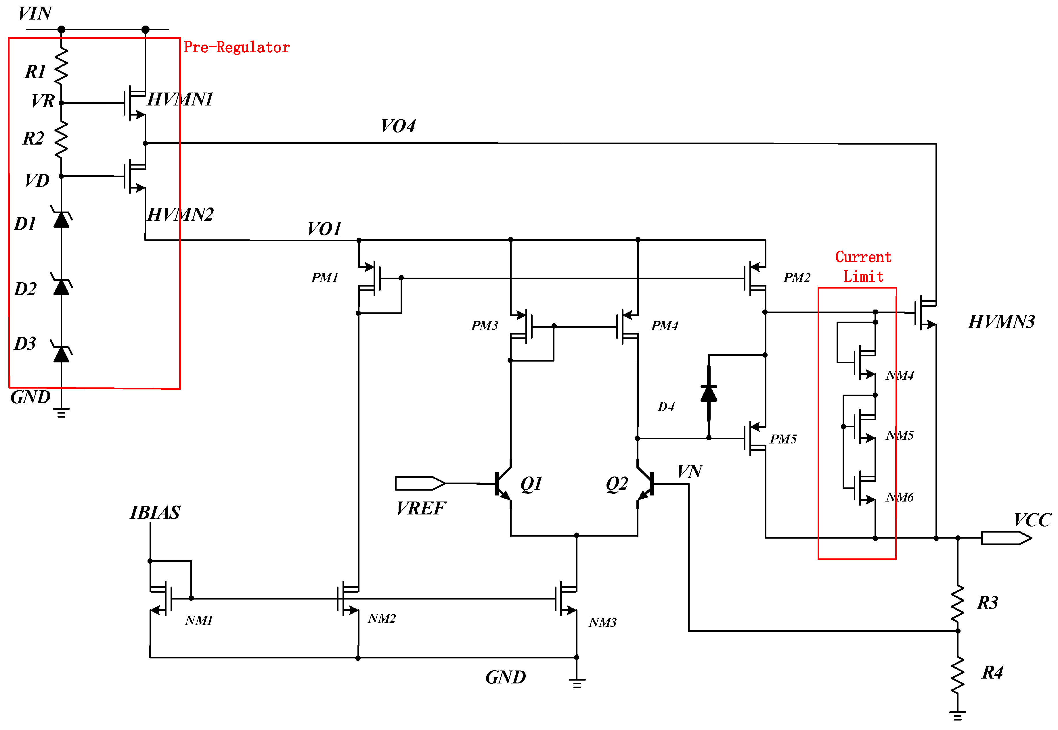
2.1. Pre-Regulator and Error Amplifier

The specific circuit of the high-voltage LDO designed in this paper is shown in Figure 4. Since the input power supply voltage may be as high as 100 V, most devices of LDO circuits are high-voltage MOS. HVMN1 and HVMN3 are 120 V LDMOS (the latter, a diffused metal oxide semiconductor), HVMN2 is 60 V LDMOS, and NM1-NM6 and PM1-PM5 are 20 V DMOS (drain-extended MOS).
R1, R2, D1–D3, HVMN1 and HVMN2 constitute a pre-regulator circuit. The R1 and R2 are narrow P+ Poly non-salicide resistors in HVNWELL, which can withstand 110 V high voltage. D1–D3 are Zener diodes. In the DB HiTek adopted in the paper, the reverse breakdown voltage of the Zener diode is 5.8 V. The principle of the pre-regulator circuit is as follows:
When the input voltage VIN gradually rises and reaches the reverse breakdown voltage of the three Zener diodes, the voltage at the VD point is:
3 × 5.8 = 17.4   V
According to the voltage of VIN and VD, the voltage of the VR point can be determined by a resistor divider. Once the VIN voltage is high enough, HVMN1 operates in the saturation region, and the voltage of VO4 is a gate source voltage VGS lower than the VR voltage. When the ratio of resistance voltage division is appropriate, HVMN2 also operates in the saturation region, and the voltage of VO1 is a VGS lower than the VD voltage. Since both PM1 and PM2 are 20 V devices and HVMN3 is a high-voltage NMOS device, their power supply voltages are different. VO1 should be less than VO4 to avoid PM1 and PM2 being damaged.
NM4, NM5 and NM6 constitute the current-limiting circuit of the LDO. NM4, NM5 and NM6 are MOS diodes connected as shown in Figure 5; that is, the gate and drain of the MOS are short connected, the source and substrate of which form a diode. The series connection of NM5 and NM6 can increase the length of the MOS; the total length is the sum of the length of NM5 and NM6. D4 clamps the gate source voltage of PM5 at its reverse breakdown voltage to prevent the breakdown of PM5.
The error amplifier can amplify the voltage difference between the reference voltage and the feedback voltage, and its performance directly affects the static and dynamic performance of the system. The gain of the EA (error amplifier) must be very high, but cannot affect the stability of the loop. At the same time, the input offset voltage in EA will affect the output accuracy of LDO system. Therefore, the EA should have low offset voltage and high gain.
The EA adopts a two-stage amplification structure. The first stage uses a BJT (bipolar junction transistor) as the input differential pair, which has a better match than an MOS (metal oxide semiconductor), reducing the input offset voltage, and improving the output accuracy of the LDO. However, the BJT is a typical current control device; the base current that cannot be ignored will generate errors. The positive input voltage of the EA, VREF is 2.5 V of the zero temperature voltage generated by the bandgap reference.
The structure of the second stage amplifier determines the range of the output voltage of the EA, and thus determines the variation range of the gate voltage of the MOS. Therefore, the minimum size of the power transistor can be obtained through the structure of the second stage amplifier. Generally, the second stage amplifier can only be selected as a common source amplifier and a source follower. The lowest power supply voltage of the second stage determines whether the source follower can be used.
According to the analysis of the voltage range at the gate of the power transistor, it can be seen that the second stage amplifier is not suitable to use an NMOS transistor as the source follower of the input MOS. When the power supply voltage is less than twice the threshold voltage of the PMOS transistor, the second stage amplifier cannot adopt the structure of the source follower. The power supply voltage in this paper is far more than twice the threshold voltage of a PMOS transistor, so the source follower of a PMOS transistor is selected in this paper.
As can be seen from Figure 4, the low-frequency voltage gain of the first stage of the EA circuit is:
A V 0 v o v id = G M ( R O | | R LOAD ) = g m 1 ( r O 2 | | r ds 4 | | R LOAD )
In Equation (2), v o is the output voltage of the first stage amplifier, R O is the parallel connection of the output resistance of Q2 and PM4, G M is the ratio of v id and the output current of the first stage, when the output voltage v o is equal to 0. Since load capacitances C LOAD often include one or more gates, the load capacitances C LOAD and the gate source capacitances C GS will be the first to shunt the resistors straddled at their ends r ds or higher at lower frequencies. R LOAD is the gate input impedance of PM5, and the resistance value is very large, so it can be ignored in the parallel relationship of Equation (2). Since the resistance value of R LOAD and r ds in the integrated circuit is typical or higher, the C LOAD resistance is shunted together with the R O R LOAD with the parasitic capacitances of Q2 and PM4 at the output node of the first stage, and a main pole limiting the bandwidth is established; that is, the output pole p o :
1 s ( C LOAD + C bc 2 + C GD 4 + C DB 4 ) | p O 1 2 π ( R O | | R LOAD ) C EQO R O | | R LOAD = r O 2 | | r ds 4 | | R LOAD
where C EQO is the equivalent capacitance at the output node of the first stage. Another group of capacitors are shunted at the gate of the current mirror to generate mirror poles p M . This is obtained by shunting the PM3 resistor 1 g m 3 connected to the diode and other parallel resistors by the parasitic capacitances of PM3, PM4 and Q1:
1 s ( C GS 3 + C GS 4 + C GD 4 + C bc 1 + C DB 3 ) 1 s ( 2 C GS 3 ) | p M g m 3 2 π ( 2 C GS 3 ) 1 g m 3 | | r ds 3 | | r ds 1 1 g m 3
In Equation (4), 1 s ( C G S 3 + C G S 4 + C G D 4 + C b c 1 + C D B 3 ) is the reactance of all capacitance which generates p M , the C GS is much larger than the gate drain capacitance C GD and the drain body capacitance C DB , C GS 3 is equal to C GS 4 . According to the analysis of the pole, the equivalence of capacitance at PM3 is close to or lower than the resistance impedance here, and the gain will decrease. It is reasoned that PM3 matches PM4, and 1 g m 3 is much smaller than both r ds 3 and r ds 1 . Therefore, even though 2 C GS 3 is quite large, the mirror pole p M is usually located at the high frequency because 1 g m 3 is small.

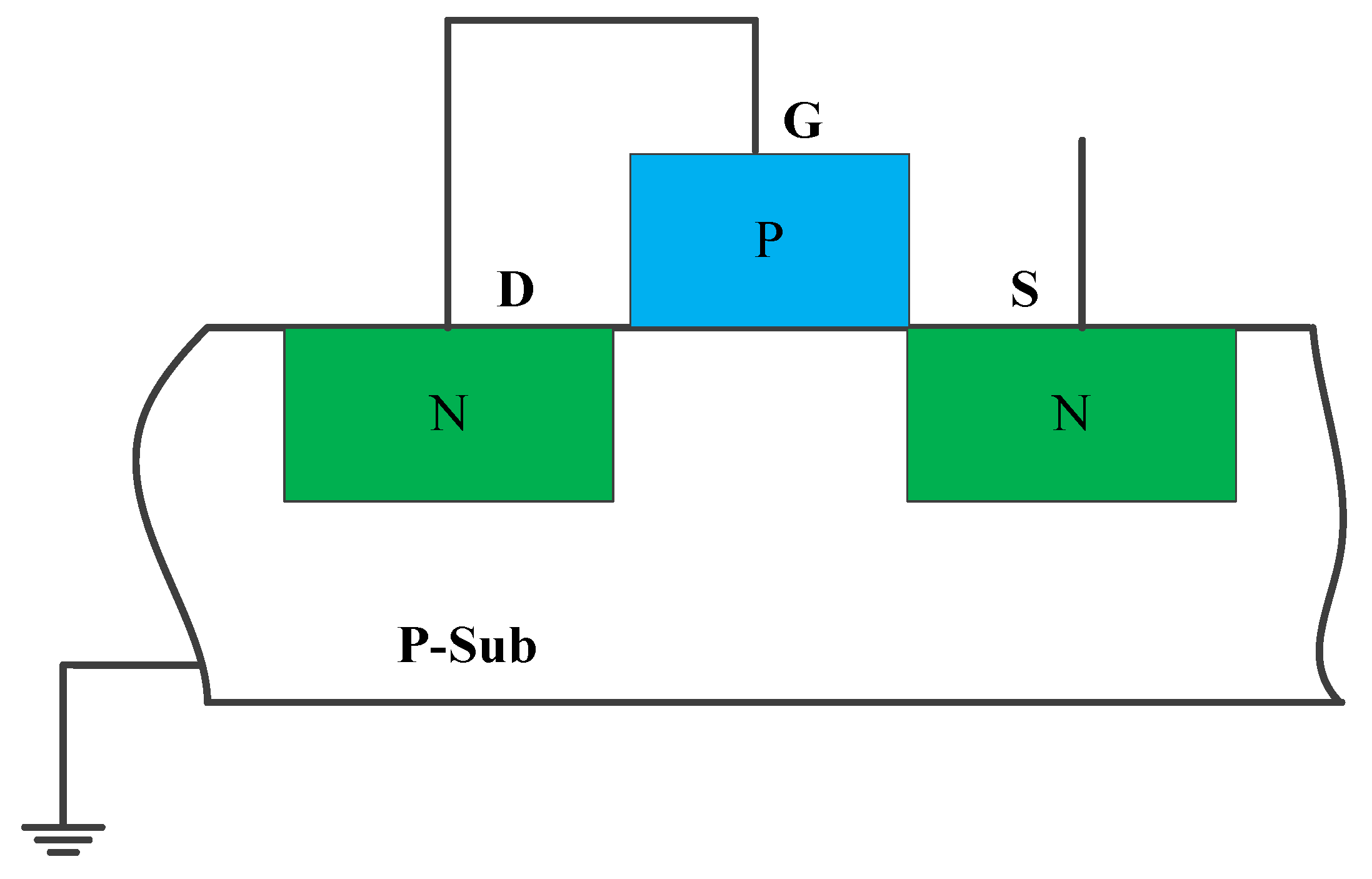
2.2. Power Transistors

There are usually two kinds of MOS transistors with operating voltages in the CMOS process. For them, the low-voltage transistors are used to construct the core circuit to achieve lower power consumption and higher operation speed, and the high-voltage transistors are used to constitute the input/output circuit of the chip, obtaining better signal transmission characteristics and reducing the energy loss on the connection between chips. Compared with a PMOS power transistor, an NMOS power transistor consumes less power transistor area when driving the same load current, which reduces the parasitic capacitance of the gate.
In general, the NMOS has the following advantages as a power transistor. Firstly, the electron mobility is higher than the hole mobility, so the size of the power transistor can be significantly reduced under the same maximum output current specification. Secondly, as the LDO of an NMOS, the transistor source is directly connected to the output node, which is actually a source follower with “local feedback”, which can provide better dynamic performance in the large signal domain. Therefore, an NMOS is used as the power transistor of LDO in this paper.

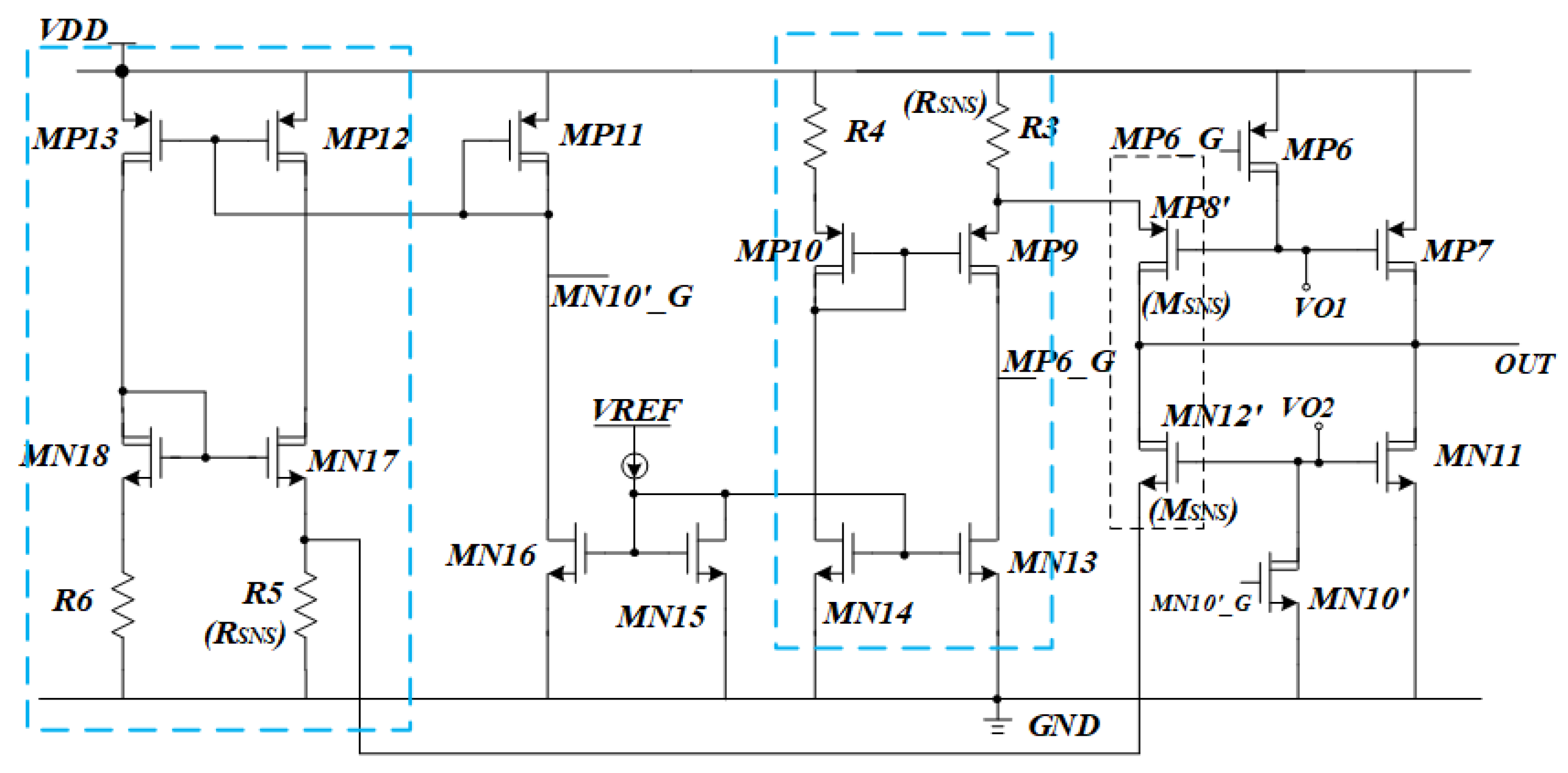
2.3. Current Limiting Technique

As shown in Figure 4, the current-limiting circuit proposed in this paper is based on the square ratio formula of the MOS in the saturation region realized by diodes, and converts the changes in the load current to the change in the gate source voltage of the MOS transistor. When the gate source voltage increases to a certain value (the reverse bias voltage of the Zener diode) due to the increase in the load current, the diode clamps the gate source voltage of the MOS transistor at the reverse bias voltage, so as to protect the power transistor. The specific working principle is: when the load current increases, the current flowing through HVMN3 will increase too. If the HVMN3 is in the saturation region at this time, it can be seen from the square rate formula of the saturation current of MOS that the change in VGS-VTH is proportional to the leakage current IDS when the aspect ratio of the MOS is constant. Thus, VGS-VTH increases with the increase in the drain current, when the VGS voltage exceeds the reverse breakdown voltage of the Zener diode D4 (the diode breakdown voltage of the process used in the paper is 5.8 V). The gate source voltage of HVMN3 will be clamped at 5.8 V (as long as the reverse current does not exceed the maximum allowable range when the reverse voltage is applied, the Zener diode will not be damaged due to thermal breakdown).
When the load current increases to the current-limit point, it is equivalent to a small resistance connected in parallel with the VCC, and the VCC is pulled down to the ground, so that the source of the HVMN3 is grounded. At this time, the VGS voltage increases to the reverse the voltage of the Zener diode, and the gate source voltage VGS of the HVMN3 is clamped to 5.8 V, so as to protect the gate oxide of the HVMN3 transistor from breakdown and keep the drain current of the HVMN3 at the current limit point. When the load current decreases, the whole system will work again and the VCC will be regulated to the voltage point that was set.

3. Simulation and Measurement Results

3.1. Simulation Result and Analysis

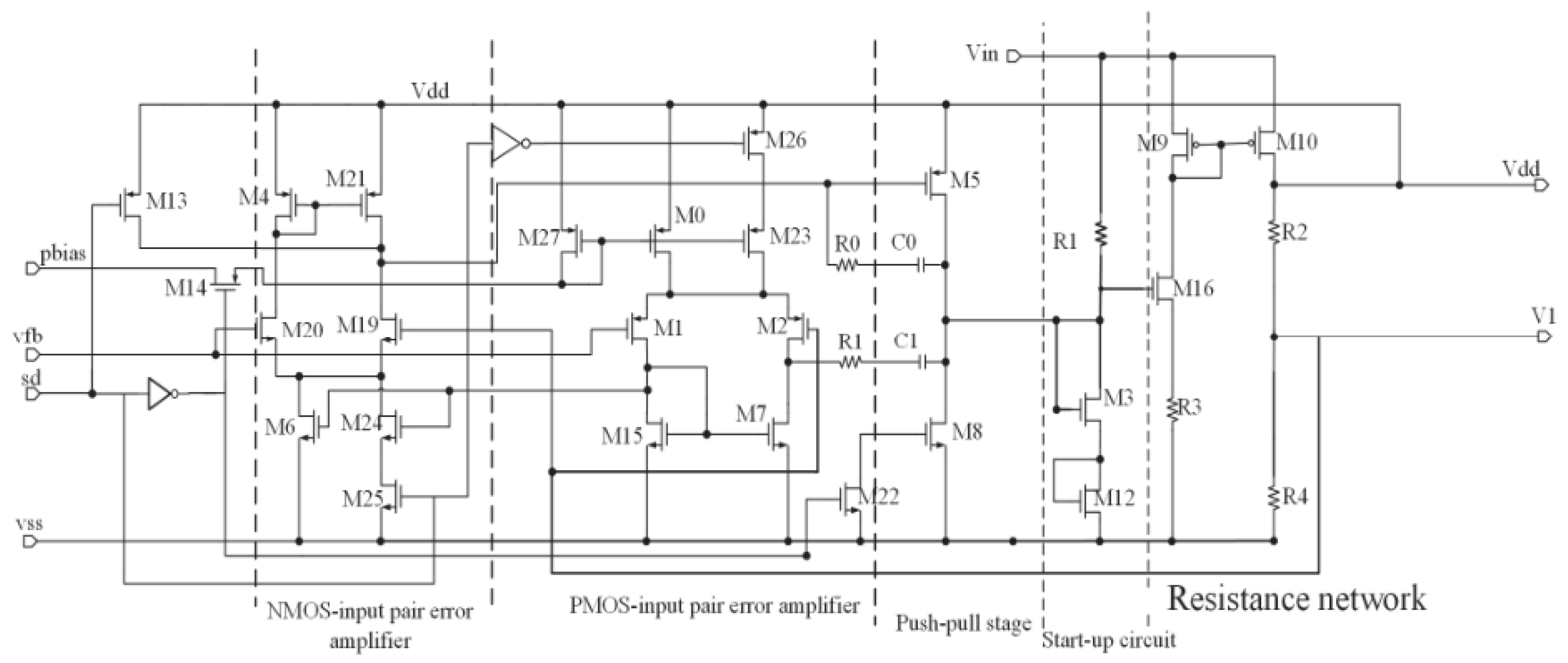
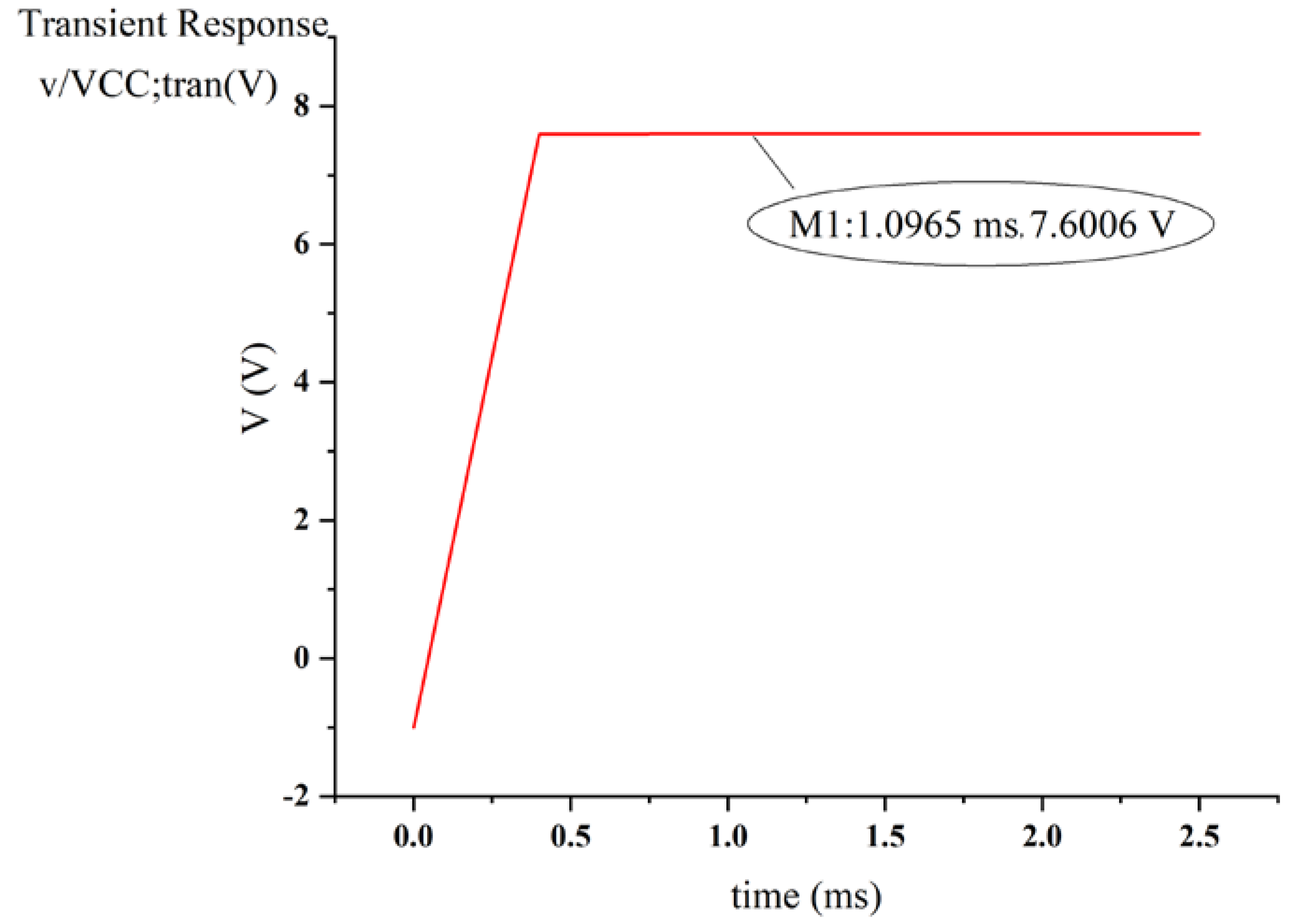
3.1.1. Startup Simulation

The startup simulation was implemented using the Cadence ADE tool with VIN = 40 V and Iload = 10 mA (TT, 27 °C). The simulation result in Figure 6 shows that the LDO could output 7.6 V. The start-up time of the circuit in Figure 6 was 498 μs.

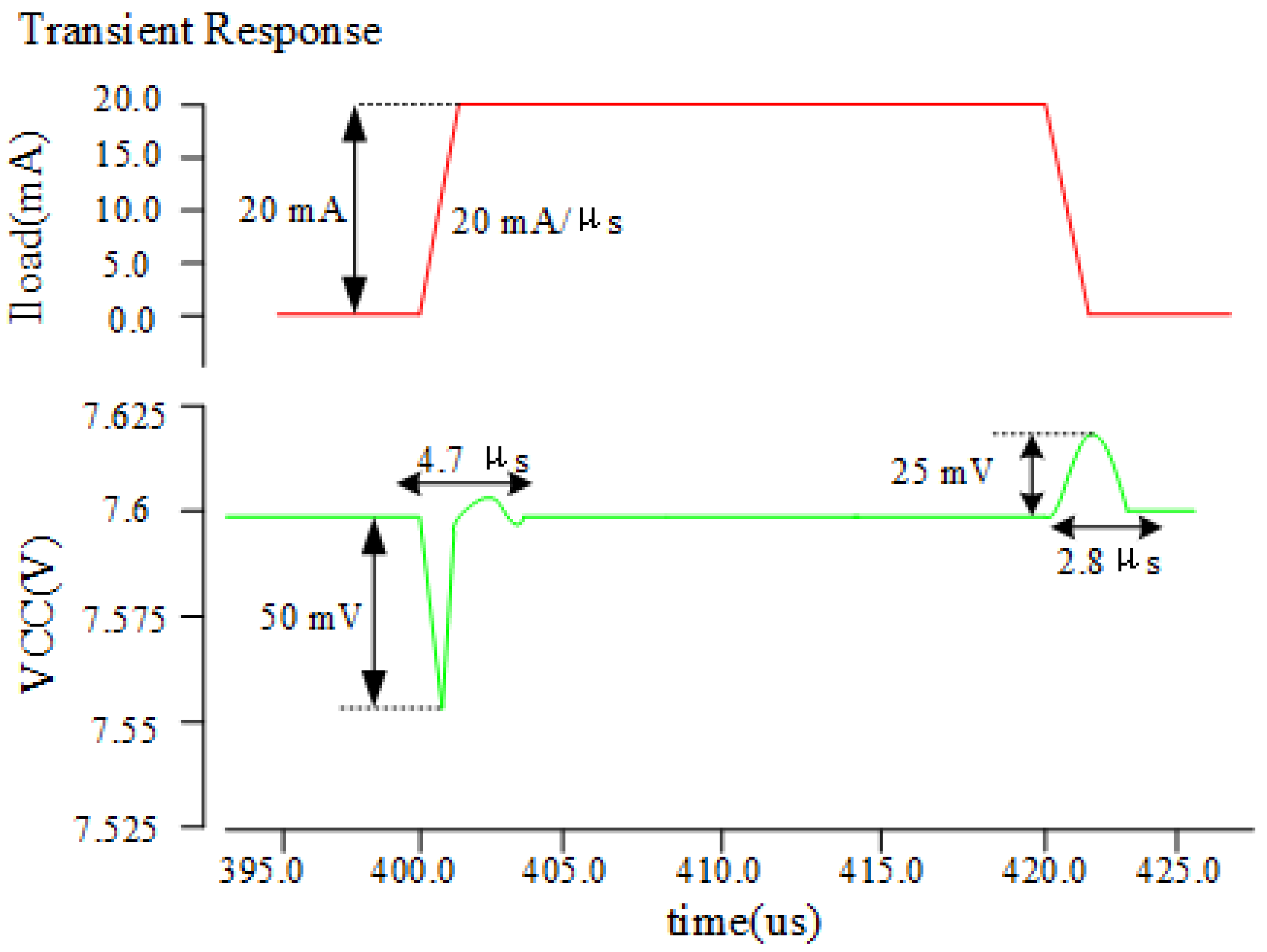
3.1.2. Transient Response

The transient response simulation was implemented using the Cadence ADE tool with VIN = 40 V, Iload jumping from no-load to 20 mA or the reverse (TT, 27 °C). Figure 7 shows the change in the LDO output voltage when the LDO load jumped (20 mA/μs). It can be seen that the LDO undershoot voltage was 50 mV, the response time was approximately 0.3 μs, and the establishment time was approximately 4.7 μs when the load jumped from no-load to 20 mA. When jumping from 20 mA to no-load, the overshoot voltage was 25 mV, the response time was approximately 1 μs, and the establishment time was approximately 2.8 μs.

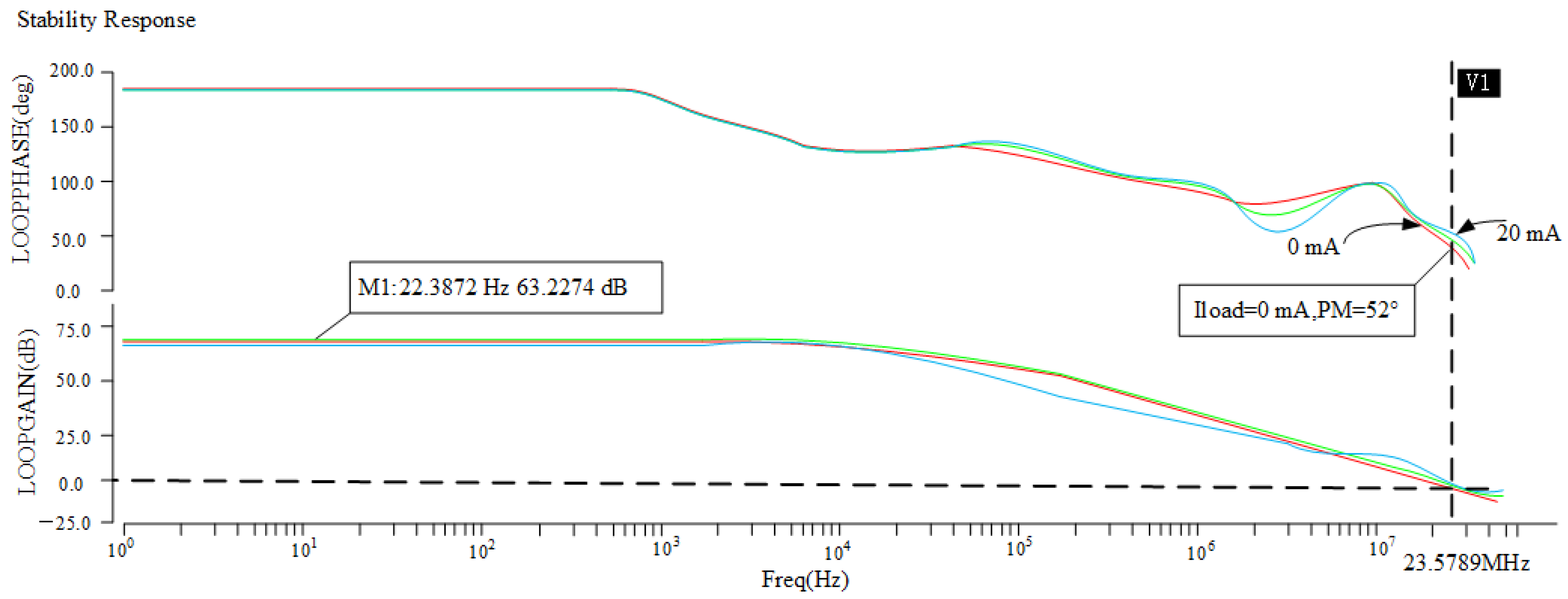
3.1.3. Loop Stability

The loop stability simulation was implemented using the Cadence ADE tool with VIN = 40 V, the Iload varied with no-load, 10, 20 mA (TT, 27 °C). Firstly, the loop at the feedback resistance network had to be disconnected, then the loop stability simulation for the LDO was conducted under the condition of load currents of 0/10/20 mA. The simulation results are shown in Figure 8. The three waveforms are the gain and phase simulation diagrams of 0/10/20 mA loads, from left to right, respectively. It can be seen from Figure 8 that the loop gain of the LDO designed in this paper under no-load was 63.2 dB, and the phase margin was 52°. With the increase in load current, the output pole moved to a higher frequency, and the phase margin of the loop also increased slightly. Since the load current did not increase greatly, the change in the phase margin was not obvious. In general, the LDO had good loop stability within the normal working load range.

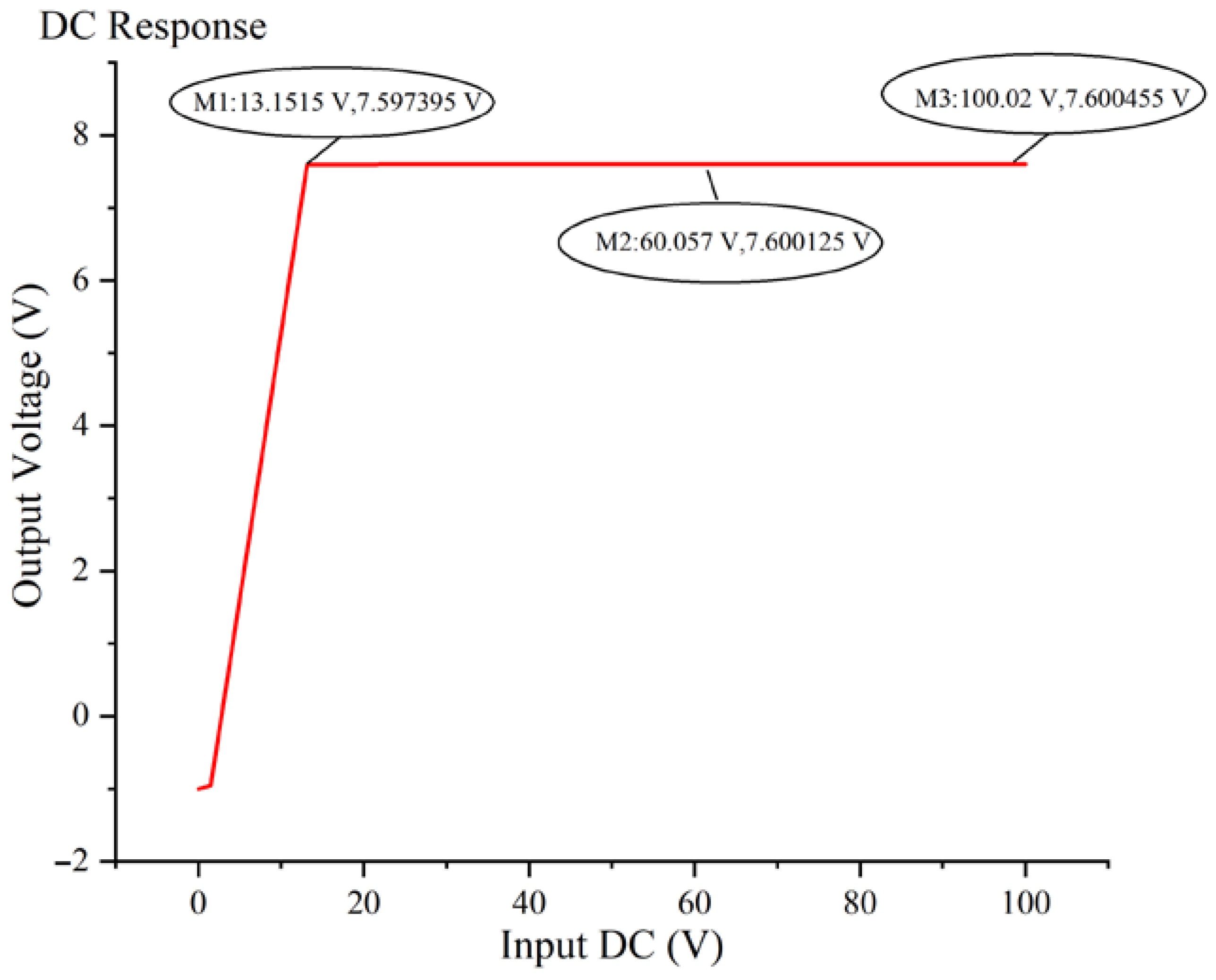
3.1.4. Line Regulation

The line regulation simulation was implemented using the Cadence ADE tool with the VIN varied from 0 V to 40 V, the Iload = 10 mA (TT, 27 ℃). The simulation waveform of the line regulation of the LDO is shown in Figure 9. The input voltage was from 13 V to 100 V, the maximum fluctuation of the output voltage was 3.06 mV, and the line regulation was 0.035 mV/V.

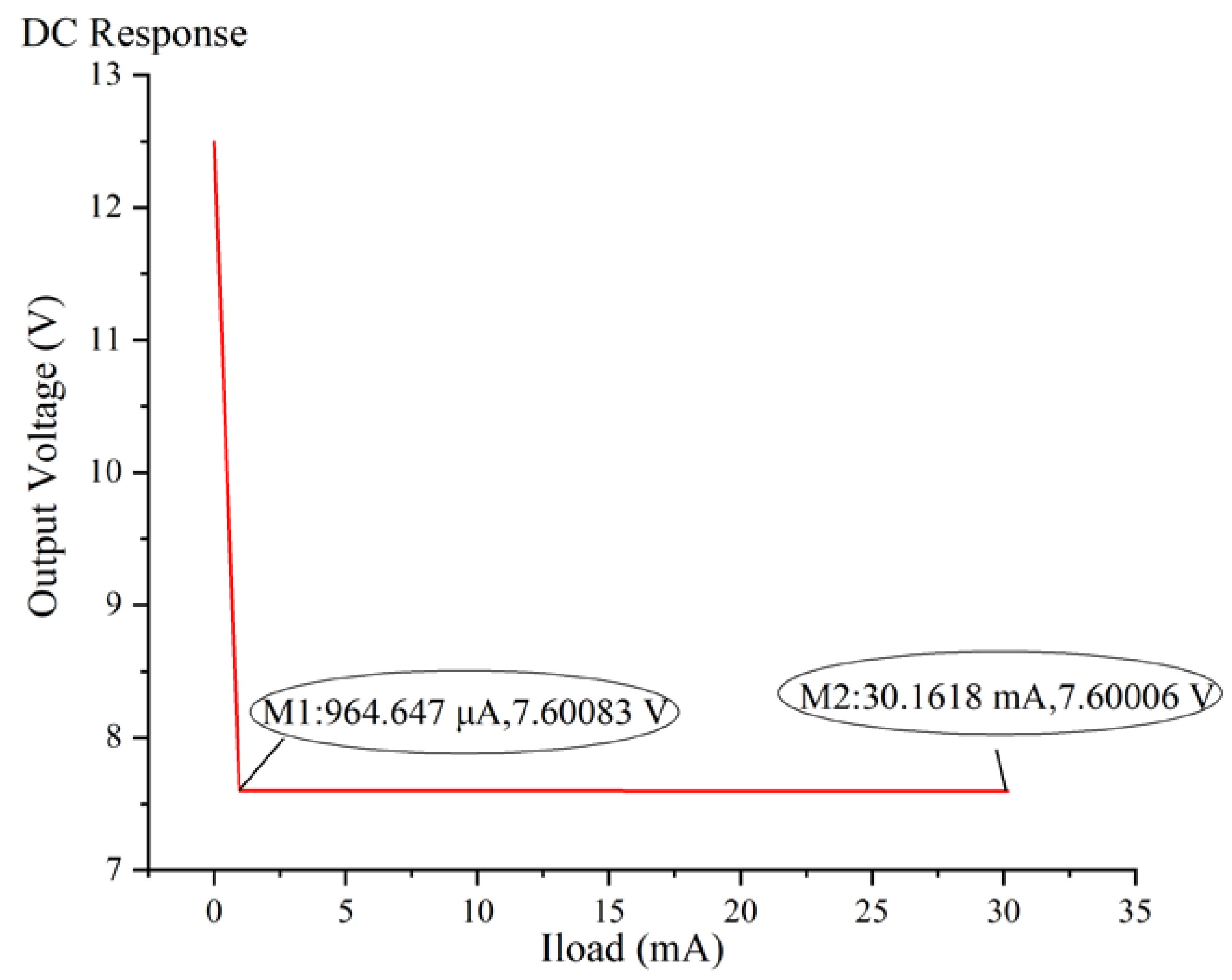
3.1.5. Load Regulation

The load regulation simulation was implemented using the Cadence ADE tool with VIN = 40 V, and an Iload varied from 0 to 30 mA (TT, 27 °C). The load regulation simulation of the LDO is shown in Figure 10. When the load current increased from 0 to 30 mA, the maximum voltage fluctuation of the output voltage was 0.77 mV, and the load regulation was 0.0256 mV/mA.

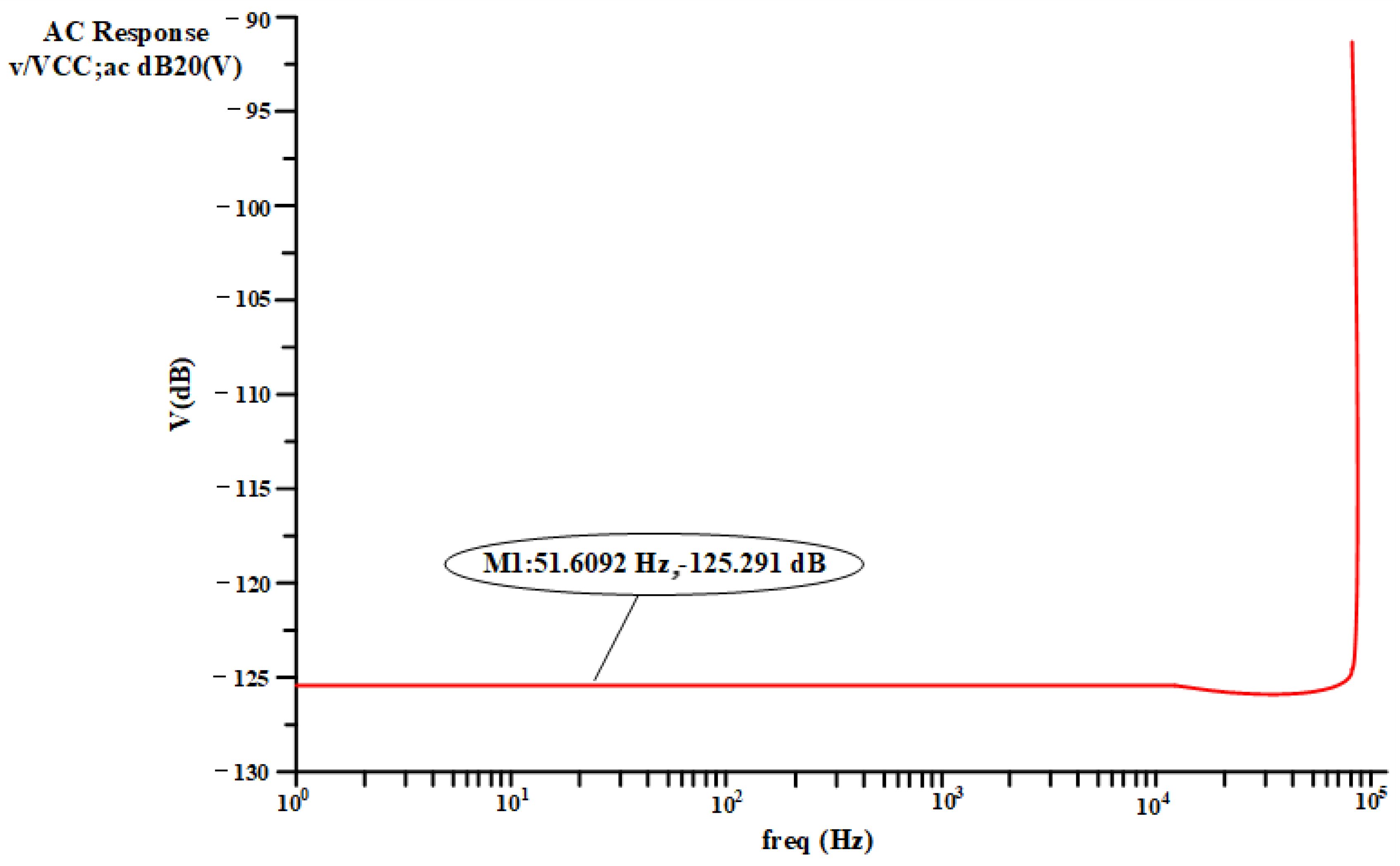
3.1.6. PSRR (Power Supply Ripple Rejection)

In order to verify the ability of the LDO output voltage designed in this paper to reject the power supply ripple, the PSRR of the LDO output voltage was simulated. The PSRR (power supply ripple rejection) simulation was implemented using the Cadence ADE tool with VIN = 40 V, there was a voltage of AC = 1 V, Iload = 10 mA (TT, 27 °C). Figure 11 shows the simulation waveform of the PSRR when the input voltage was 40 V and the load current was 10 mA. The influence of the power supply voltage change on power supply ripple rejection was mainly reflected in the low frequency range. It can be seen from Figure 11 that the PSRR at low frequency was −125 dB, which shows good power supply rejection capability.

3.1.7. Current Limit

To verify the LDO current-limiting function, the chip overcurrent was simulated by changing the output load current under DC simulation. The current-limiting simulation was implemented using the Cadence ADE tool with VIN = 40 V, and the Iload was variable to sweep until VCC dropped to 0 V (TT, 27 °C).
It can be seen from the simulation waveform in Figure 12 that the circuit proposed could limit the current of the power MOS to 34 mA; that is, the current-limiting circuit can protect the output from overloading.

3.2. Measurement Results

The high-voltage LDO in the paper was implemented in a DB HiTek 0.18 μm BCD process, and the LDO was then used in the DC-DC chip. The layout of the high-voltage LDO is shown in Figure 13, and the size was 660 × 330 μm. In addition, the micro-photograph of the pre-regulator and LDO are shown in Figure 14.
The current-limiting protection circuit is shown in the purple box in Figure 13, which shows the MOS diode connected. The layout size was 160 × 40 μm.
Table 1 shows the measurement results of the maximum load current of the LDO at room temperature (27 °C). The maximum load current during simulation was 30 mA, and the maximum load current of the actual chip was about 19 mA.
Due to the requirements of practical applications, the magnitude of the output voltage and maximum load current may be different from the simulation results. We redrew the measurement results in Table 1 as shown in Figure 15. Because there was noise in the actual environment and the sensitivity of the test instrument, the output voltage at 20 mA was −0.05 V.
Table 2 shows the measurement results of the LDO designed at room temperature (27 °C). The range of the VIN was from 20 V to 85 V, and the voltage fluctuation of VCC was monitored.
Figure 16 shows the test results of the maximum input voltage of the LDO. The maximum input voltage of the LDO was the sum of the voltage values shown in the middle and lower voltmeters of Figure 16. Figure 16a–c show the test conditions under which the input voltage was 130, 135 and 140 V, respectively. The upper voltmeter in Figure 16 shows the output voltage of the LDO.
The test data of Figure 16 was sorted into Table 3. It can be seen from Figure 16c that when the input voltage was 140 V, the VCC voltage was stable; that is, the LDO could work normally.
Due to noise interference from the test environment and the sensitivity of the measurement instrument, the measurement values of the line and load regulation were lower than the simulation values. From the data in Table 3, the LDO can withstand a 140 V high-voltage input, but it was only set to 100 V for the simulation, referring to the instructions of the PDK (Process Design Kit); the actual measurement value was more important for this indicator. Table 4 compares the simulation and measurement results of the LDO proposed in this paper with other data from the same type of literature.

4. Conclusions

In this paper, a novel high-voltage LDO circuit is proposed and a diode-clamped current-limiting scheme is used to protect the circuit, which has a simple structure and excellent performance. The principle of the high-voltage LDO module and a current-limiting protection circuit was analyzed in detail and verified by simulation in this paper. The high-voltage LDO was used in some portable electronic devices and was tried out using the DB HiTek 0.18 μm BCD process. The simulation results showed that the LDO can stably output 7.6 V under an input voltage from 13 V to 100 V. The load regulation rate was 0.0256 mV/mA, and the line regulation rate was 0.035 mV/V; the output voltage can be prohibited when the load current exceeds 30 mA. The measurement results showed that the maximum input voltage of the designed chip can reach 140 V. The test results agreed with the simulation. When the load current exceeded 19 mA, the LDO had no output voltage, though due to the problems of the manufacturing process and the test environment, there were differences in the test results and simulation results, which indicates that the current limiting circuit can work stably. The measurement results showed that the current-limiting circuit could stably protect the LDO under the overload condition. According to the analysis of the current data, the chip meets the design requirements at room temperature. The main work for the future will be to evaluate the performance of the chip in high temperature and low temperature environments.

Author Contributions

Conceptualization, L.L. and X.L.; methodology, L.L.; validation, L.L., D.J. and L.S.; formal analysis, L.L.; writing—original draft preparation, L.L.; writing—review and editing, D.J. and L.S.; supervision, X.L.; funding acquisition, X.L.; Data curation, S.X. All authors have read and agreed to the published version of the manuscript.

Funding

This research was funded by [the National Natural Science Foundation of China] grant number [61771363].

Data Availability Statement

Data available on request due to restrictions eg privacy or ethical.

Conflicts of Interest

The authors declare no conflict of interest.

References

  1. Ren, Y.; Huang, S.; Duan, Q.; Ding, Y.; Li, M. A 1500 mA load current LDO with wide power supply range in lithium-ion battery. In Proceedings of the 2018 13th IEEE Conference on Industrial Electronics and Applications (ICIEA), Wuhan, China, 31 May–2 June 2018; pp. 2141–2144. [Google Scholar] [CrossRef]
  2. Yin, J.; Huang, S.; Duan, Q.; Cheng, Y. An 800 mA load current LDO with wide input voltage range. In Proceedings of the 2017 International Conference on Circuits, Devices and Systems (ICCDS), Chengdu, China, 5–8 September 2017; pp. 174–178. [Google Scholar] [CrossRef]
  3. Ryzhkov, V.A.; Karpovich, M.S.; Surin, I.K.; Vasilyev, V.Y. High-voltage low drop output voltage regulator with output current fold-back protection in 250 nm BCD technology. In Proceedings of the 2016 17th International Conference of Young Specialists on Micro/Nanotechnologies and Electron Devices (EDM), Erlagol, Russia, 30 June–4 July 2016; pp. 549–554. [Google Scholar] [CrossRef]
  4. Wang, Y.; Ding, L.; Bao, Z.; Yang, H.; Jin, X. High current operational amplifier with current limiting protection circuit. IET Circuits Devices Syst. 2020, 14, 251–259. [Google Scholar] [CrossRef]
  5. Guo, J.; Leung, K.N. A fold-back current-limit circuit with load-insensitive quiescent current for CMOS low dropout regulator. In Proceedings of the 2009 IEEE International Symposium on Circuits and Systems (ISCAS), Taipei, Taiwan, 24–27 May 2009; pp. 2417–2420. [Google Scholar] [CrossRef]
  6. Matyscak, J.; Radhostem, R.P. Output Current Limiter for a Linear Regulator. US Patent US 2021/0018944 A1, 21 January 2021. [Google Scholar]
  7. Zhang, N.; Gu, J. LDO Circuit Device and Overcurrent Protection Circuit of LDO Circuit. US Patent US 2020/0333816 A1, 22 October 2020. [Google Scholar]
  8. Xiao, B.; Venkatachala, P.K.; Xu, Y.; ElShater, A.; Lee, C.Y.; Leuenberger, S.; Moon, U.K. An 80 mA capacitor-less LDO with 6.5 μA quiescent current and no frequency compensation using adaptive-deadzone ring amplifier. In Proceedings of the IEEE Asian Solid-State Circuits Conference, Macao SAR, China, 4–6 November 2019. [Google Scholar]
  9. Sakolski, O.; Poongodan, P.K.; Vanselow, F.; Maurer, L. A feedforward compensated high-voltage linear regulator with fast response, high-current sinking capability. IEEE Solid-State Circuits Lett. 2020, 3, 114–117. [Google Scholar] [CrossRef]
  10. Hu, D.; Zhang, G.; Tong, M.S. A new design for low drop-out regulator with broadband high power supply rejection. In Proceedings of the 2020 IEEE International Conference on Computational Electromagnetics (ICCEM), Singapore, 24–26 August 2020; pp. 281–282. [Google Scholar] [CrossRef]
  11. Lavalle-Aviles, F.; Torres, J.; Sánchez-Sinencio, E. A high power supply rejection and fast settling time capacitor-less LDO. IEEE Trans. Power Electron. 2019, 34, 474–484. [Google Scholar] [CrossRef]
  12. Tang, J.; Dai, C.; Ouyang, L.; Wang, Y.; Zou, W. A design of high voltage pre-regulator circuit for LED driver. In Proceedings of the 2021 9th International Symposium on Next Generation Electronics (ISNE), Changsha, China, 9–11 July 2021; pp. 1–4. [Google Scholar] [CrossRef]
  13. Ho, M.; Guo, J.; Mak, K.H.; Goh, W.L.; Bu, S.; Zheng, Y.; Tang, X.; Leung, K.N. A CMOS low-dropout regulator with dominant-pole substitution. IEEE Trans. Power Electron. 2016, 31, 6362–6371. [Google Scholar] [CrossRef]
  14. Adorni, N.; Stanzione, S.; Boni, A. A 10-mA LDO with 16-nA IQ and operating from 800-mV supply. IEEE J. Solid-State Circuits 2020, 55, 404–413. [Google Scholar] [CrossRef]
  15. Fan, S.; Li, H.; Guo, Z.; Geng, L. A 5.2 μA quiescent current LDO regulator with high stability and wide load range for CZT detectors. IEEE Trans. Nucl. Sci. 2017, 64, 1087–1094. [Google Scholar] [CrossRef]
Figure 1. The pre-regulator circuit proposed in [1].
Electronics 12 03257 g001
Figure 2. The current-limiting circuit proposed in [5].
Electronics 12 03257 g002
Figure 3. The overall structure of LDO in this paper.
Electronics 12 03257 g003
Figure 4. The specific structure of LDO in this paper.
Electronics 12 03257 g004
Figure 5. Diode connected in NMOS and PMOS.
Electronics 12 03257 g005
Figure 6. Output of the proposed LDO regulator.
Electronics 12 03257 g006
Figure 7. Simulated load transient response (VIN = 40 V, 27 °C).
Electronics 12 03257 g007
Figure 8. Loop stability simulation with 0/10/20 mA loads.
Electronics 12 03257 g008
Figure 9. Simulated line regulation of LDO.
Electronics 12 03257 g009
Figure 10. Simulated line regulation of the LDO.
Electronics 12 03257 g010
Figure 11. Simulated PSRR performances of the LDO at Iload = 10 mA.
Electronics 12 03257 g011
Figure 12. Simulated current limiting by the proposed LDO.
Electronics 12 03257 g012
Figure 13. The layout of the LDO.
Electronics 12 03257 g013
Figure 14. Micro-photograph of the pre-regulator and LDO.
Electronics 12 03257 g014
Figure 15. Test results of the proposed LDO.
Electronics 12 03257 g015
Figure 16. Measurement of the LDO.
Electronics 12 03257 g016
Table 1. Measurement results of the maximum load current of LDO.
ParametersValue
Load current (mA)0151617181920
Output voltage (V)7.7017.7017.646.786.730.7−0.05
Table 2. Measurement of the LDO output voltage vs. input voltage.
ParametersValue
VIN (V)20253035404550
VCC (V)7.65207.65167.65117.65137.65087.65097.6508
VIN (V)55606570758085
VCC (V)7.65067.65047.65057.65027.65017.65007.6500
Table 3. The measurement results of MAX VIN.
ParametersValue
VIN (V)130135140
VCC (V)7.67387.67377.6754
Table 4. Performance comparisons.
ParameterUnitThis Work[3][12][13][14][15]
SimTest
Technologynm180-18055180400250
Areamm20.2178-0.150.0420.216No1.42
Max. loadmA3019No101501500800
Supply voltageV13–100140700.82.9–3.33.9–203.9–20
Output voltageV7.67.6508660.62.82.52.5
PM°52-NoNo62.1NoNo
Line regulationmV/V0.0350.022690 (no load)0.51.25No0.5093
Load regulationmV/mA0.02560.00031.71.050.250.00130.0458
PSRR (@1 kHz)dB−125-No42.7<−50NoNo
Disclaimer/Publisher’s Note: The statements, opinions and data contained in all publications are solely those of the individual author(s) and contributor(s) and not of MDPI and/or the editor(s). MDPI and/or the editor(s) disclaim responsibility for any injury to people or property resulting from any ideas, methods, instructions or products referred to in the content.

