Abstract
Electric Vehicle (EV) wireless power transfer technology is an excellent solution to propel EVs forward. The existing wireless power transfer technology for EVs based on Inductive Power Transfer (IPT) technology has the drawbacks of large size, high weight, and high eddy current loss, limiting the further application of this technology. Capacitive Power Transfer (CPT) technology, with its advantages of low cost and light weight, has attracted widespread focus in recent years and has great potential in the field of EV wireless power transfer. This paper begins with the principle of CPT, introduces the potential and development history of CPT technology in the field of EV wireless power transfer, and then reviews the coupling mechanism and resonance compensation network of the CPT system to satisfy the requirements of EV wireless power transfer, including the coupling mechanism of EV static power transfer and dynamic power transfer, and the high-performance resonance compensation network to the requirements of EV wireless power transfer. Finally, this paper reviews the existing problems of CPT technology in the field of EV wireless power transfer and summarizes its future development directions.
1. Introduction
Electric Vehicles (EVs) are of great significance to the development and progress of the current era, as they have the potential to reduce pollution, alleviate the energy crisis, and reduce transportation costs [1,2,3,4]. Until now, EVs have almost always been powered by plug-in power supplies, which have many drawbacks. The first drawback is that plug-in power supplies have wear and tear problems, affecting their service life; the second is that the large-capacity batteries on the body add to their weight and cost [5,6,7,8]. These drawbacks greatly limit the further development of the EV industry. That is why the development of wireless power transfer for EVs, allowing electrical power to be transferred to EVs without contact, is crucial to the further development of EVs. Near-field wireless power transfer technologies can be classified into two types: Inductive Power Transfer (IPT) and Capacitive Power Transfer (CPT). IPT technology has been widely utilized in EV power transfer [9,10,11,12]. Despite this, the unavoidable problems of IPT technology, such as large size, high weight, and the presence of eddy current losses, make it difficult to achieve further development. The CPT system, however, with its low weight and size and negligible eddy current losses, has tremendous potential in the field of EV wireless power transfer. CPT technology has been regarded as only capable of transmitting small power with large losses for an extended period [13,14]. However, with the continuous deepening of research regarding CPT technology in recent years, especially the continuous development of high-power and high-efficiency CPT technology, the power level and efficiency of CPT systems have been significantly improved [15]. It is an essential potential solution for EV wireless power transfer. Almost all of the existing reviews on the field of EV wireless power transfer are mainly on IPT [16], with only a summary of CPT technology in the field of EV wireless power transfer [17,18,19]. At the same time, the existing review on CPT technology is mainly an overview of almost the whole field of CPT technology research [20], where the applications of this technology in the EV wireless power transfer field are only briefly summarised as one of the chapters [21,22]. In conclusion, in the existing literature, there is no general review of the application of CPT technology to EV wireless power transfer in a concrete and elaborate sense. This paper, being the first systematic and comprehensive review to summarise the application of CPT technology in the field of EV wireless power transfer, begins with the principle of CPT technology and introduces the potential of CPT technology for EV wireless power transfer field application and the history of its development. Different from the conventional CPT system, a CPT system suitable for EV wireless power transfer requires larger power transmission, so the coupling mechanism and resonance compensation network need to be improved. Therefore, this paper further discusses the coupling mechanism and resonance compensation network of a CPT system for EV wireless power transfer applications and provides a reference for CPT system selection. It is worth mentioning that IPT technology currently dominates the market, while CPT technology is still in the early stages of commercial adoption. For this reason, this paper analyses the existing challenges of current CPT technologies and eventually proposes solutions and development directions to overcome these challenges. The overall framework diagram of this paper is shown in Figure 1.
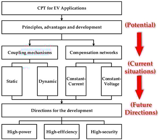
Figure 1.
The overall framework diagram of this paper.
2. The Potential and Development History of CPT Technology for EV Applications
2.1. CPT System Working Principle
CPT technology uses a high-frequency electric field to transfer power contactlessly. Its structure is shown in Figure 2 [20,23,24]. Its principle is that the DC power is converted to high-frequency AC power by the inverter. It flows into the coupling mechanism through the original side LC compensation network. Under high-frequency and high-voltage AC power, the coupling mechanism’s primary and secondary coupling pole plates are equivalent to a set of flat capacitors. At the same time, an electric field is formed between them, which generates a “displacement current”, so the power is transferred from the coupling mechanism’s primary pole plates to the coupling mechanism’s secondary pole plates, thus enabling non-contact power transfer. After passing through the secondary LC compensation network and rectifier, it is converted into suitable power for the load [21,22,25].
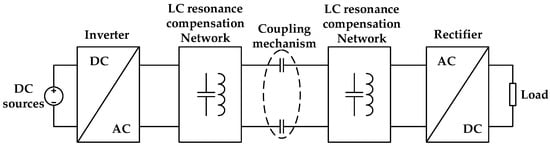
Figure 2.
CPT system structure.
2.2. Advantages of CPT Technology in Comparison to IPT Technology
Although IPT technology has already made a significant achievement in the field of EV wireless power transfer, it still suffers from the following shortcomings due to its own principles.
- The primary material of the IPT system coupling mechanism is litz wire, which is more costly [26];
- Frequently, IPT systems rely on ferrite, which is expensive, heavy, and fragile, and ferrite’s high-frequency loss limit makes IPT systems unsuitable for megahertz levels of high frequency, so they tend to have larger sizes and are harder to embed in the ground [27];
- In IPT systems, large eddy current losses cause heat to be generated in metals in the surroundings, which increases fire risks [28];
- During long-term operation, IPT systems generate heat due to losses in the coupling coil, resulting in the need for additional heat sinks and an increase in system complexity and cost.
However, the CPT system relies on the electric field for power transmission; the coupling mechanism consists only of a relatively inexpensive metal plate, does not require ferrite, works in high-frequency environments, is small in size, and can be integrated into the ground. Furthermore, the CPT system is insensitive to metal objects. It will not interfere with foreign objects in the surrounding area, and since the electric field has better directivity, it will also be more effective at preventing diversion [29,30]. As a result, CPT technology offers more significant potential in the area of wireless power transfer for EVs than conventional IPT technology [31,32].
2.3. Development History of CPT Technology for EV Applications
The development of CPT technology for EV applications is shown in Figure 3.

Figure 3.
The development history of CPT technology in the field of wireless power transfer for EVs.
The initial research on the wireless power transfer using CPT technology in the EV field originated from a patent proposed by Jeffrey A. Rose, an American scholar, in 1998, which increased the equal coupling capacitance by attaching a medium between the coupling plates and achieved a theoretical power output of 9 kW through theoretical analysis [33]. However, limited by the overall development of CPT technology, this patent only proposes a wireless power concept, and no follow-up research has been conducted.
In 2011, Takashi Hira’s team at Toyohashi University of Science and Technology, proposed the idea of using CPT technology for the wireless power transfer of EVs and, in 2013, built an experimental platform that could power a small uncrewed EV [34,35] and placed the coupling mechanism inside the wheels of the EV to provide 60 W of wireless power to the tested EV. This opened the door for CPT technology to be applied to EVs. However, the study was only a technical validation, and its system power level was significantly below the power level required for daily crewed EVs.
In 2015, Daniel C. Ludois’ team at the University of Wisconsin–Madison placed a coupling mechanism at the bumper of an EV. It enabled the first power transfer to a crewed small EV by fastening it to a flexible foil, transmitting 1021 W of power [36]. This opened the way for applying CPT technology in the high-power area. However, this application was limited to crewed small EVs. The power level still fell short of the power requirements for daily-traveling crewed EVs.
In 2015, Chunting Chris Mi’s San Diego State University team proposed a scheme to place the coupling mechanism at the chassis of the EV. It used a double-sided LCLC-type resonance compensation network to achieve a power output of 2.4 kW, upgrading CPT’s power transfer power level to 2 kW [37]. It kicked off the research of CPT technology in high power and provided the solution of CPT for EV power transfer.
In 2016, Takashi Ohira’s team at Toyohashi University of Technology modified a small human-carrying EV by placing power receiver plates at the wheels of the EV, extending the length of the power transmitter plates, and mounting them inside the roadway. It was the first time that dynamic power transfer of CPT technology to a crewed small EV was achieved, traveling at a speed of 10 km/h for 4 m [38], opening the way for the dynamic EV wireless power transfer with CPT technology.
In 2018, Mitsuru Masuda at Furukawa Electric developed metal shielding boxes for the coupling plates to minimize electric field dissipation during power transfer. This significantly improved the CPT system’s security. The team transmitted kilowatts of power over a distance of 70 mm for a crewed small EV, reducing the electric field dissipation in all directions of the coupling mechanism [39], making EV wireless power transfer more secure.
Nowadays, with the continuous development of the theory, structure, and components of CPT technology, CPT technology for EV wireless power transfer applications is moving rapidly towards the development of high power, high efficiency, and high security.
3. Coupling Mechanism
3.1. Coupling Mechanism Equivalent Mode
Figure 4 shows that the ideal CPT coupling mechanism equivalent model has only two coupling capacitances, one for power transfer and the other for power return [40]. These two equal coupling capacitances form a double-capacitance structure, as shown in Figure 4b. Considering that the two coupling capacitances are connected in series, they can be further equated to a single capacitance, as shown in Figure 4c.
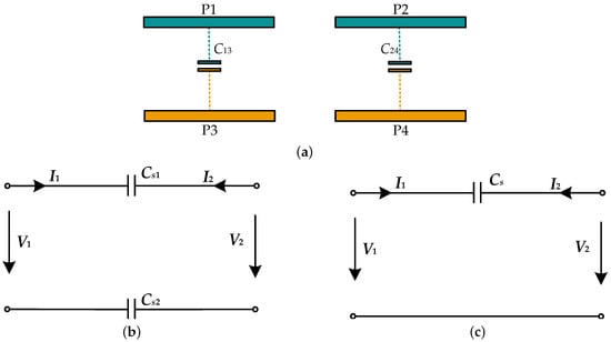
Figure 4.
The ideal CPT coupling mechanism equivalent model: (a) two equivalent capacitances of the ideal model of the CPT coupling mechanism; (b) double-capacitance structure; (c) single-capacitance structure.
In practice, however, the CPT coupling mechanism can generate six equal coupling capacitances, as shown in Figure 5. The four extra coupling capacitances include the self-capacitance generated by the mutual coupling of the plates on the same side, such as and in Figure 5, and the cross-coupling capacitance between the “transmitter–receiver” plates of different power transmission channels, such as and in Figure 5.
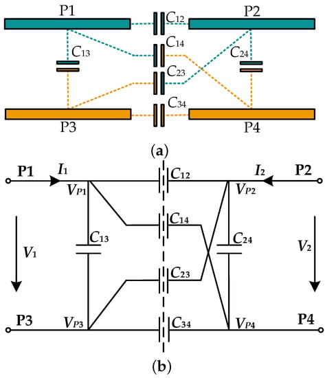
Figure 5.
Equal six-capacitance model of the CPT coupling mechanism: (a) six equivalent capacitances of the equal six-capacitance model of the CPT coupling mechanism; (b) two-port network for six-capacitance models.
The six-capacitance system most accurately reflects self-capacitance distribution, mutual-capacitance, and cross-coupling capacitance between coupling mechanisms. However, the system involves a large number of capacitances and complex line connections, making it more challenging to perform topological analysis.
3.1.1. /T-Type Network Model
Using this two-port network model with six capacitances, the voltage–current relationship between the two sides can be represented as the combined effect of the self-capacitance and the mutual-capacitance. Additionally, the six-capacitance model can be converted into an equal network model composed of two self-capacitors and one mutual-capacitance using Equation (1) [41,42]. According to the T- conversion relationship, the -type equivalent model can be converted into a T-type equal network model according to Equation (2) [43], as shown in Figure 6.
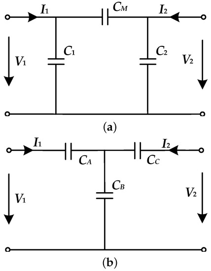
Figure 6.
Equal /T model of CPT coupling mechanism: (a) the -equivalent model; (b) the T-equivalent model.
3.1.2. ICS/IVS Model
For the six-capacitance model, the transmitter and the receiver of the coupling pole plate can be regarded as a “whole”, and the two “whole” transmitters and receivers can be connected by introducing the concept of “mutual-capacitance”. At the same time, equal current sources can replace the transmitter and receiver. The coupling capacitance at both ends is expressed as total capacitance, and the ICS (Induced Current Source) equivalent model is obtained [44]. The equal total capacitance at both ends is shown in Equation (3), and the equation for the equal current source is shown in Equation (4). The ICS model can be converted to the IVS (Induced Voltage Source) model by the transformation of Equation (5), as shown in Figure 7 [45].
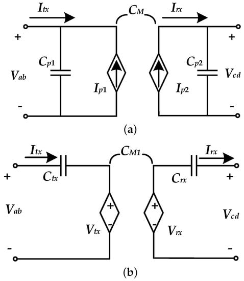
Figure 7.
Equal ICS/IVS model of CPT coupling mechanism: (a) the ICS model; (b) the IVS model.
The comparison of several different equal modes is shown in Table 1.

Table 1.
Comparison of the characteristics of several equivalent models.
Table 1 shows that a suitable coupling mechanism equal model should be reasonably selected according to the accuracy required, the content analyzed, and the computational complexity. In this paper, the -type network model is applied to the coupling mechanism in the later analysis because of the requirements of a high-precision model, more emphasis on the analysis of resonance relationships, and the demand for a simple degree of model computation.
3.2. Coupling Mechanism Placement in Static Power Transfer Scenarios
In the static power transfer scenarios, the coupling mechanism placement mode can be broadly classified into three categories:
- Equivalent capacitance mode using a large air gap;
- Equivalent capacitance mode using EV’s body structure;
- Equivalent capacitance with a coupling mechanism attached to the EV body surface.
3.2.1. Equivalent Capacitance Mode Using a Large Air Gap
The power transmitter side of the coupling mechanism is installed on the ground, and the power receiver side is located inside the EV. The air is used as a medium for transmitting power. The equivalent capacitance is calculated as shown in Equation (6), where and are the vacuum dielectric constant and the relative dielectric constant of the capacitive medium, respectively, S is the equivalent facing area of the capacitive pole plate, and d is the equivalent orthogonal distance of the capacitive pole plate.
Due to the considerable distance between the EV chassis and the ground, it is often necessary to increase the area of the coupling pole plate to couple out large capacitances. As a result of this mode, the coupling plates tend to have large dimensions, increasing the cost of the coupling mechanism. Despite this, as the receiver pole plate is placed at the chassis of the EV, it does not affect the appearance or performance of the EV, and it is also convenient for the maintenance personnel to overhaul the coupling pole plate.
The equivalent capacitance mode that uses a large air gap can be divided into the four-plate parallel structure, four-plate vertical structure, and two-plate vertical structure according to the structure of the coupling mechanism and the number of plates, as shown in Figure 8.
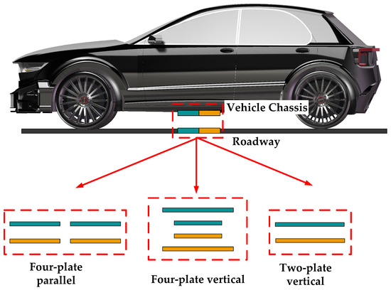
Figure 8.
The equivalent capacitance mode that uses a large air gap.
In the four-plate parallel structure, two transmitter plates are placed on the road in the same plane parallel to each other, and two receiver plates are placed at the chassis of the EV in the same way, as shown in Figure 9 [37]. In operation, one set of transmitter–receiver pole plates plays the role of power transfer, and the other set of transmitter–receiver pole plates plays the role of power return [46]. The advantage of this scheme is that the influence between the transmitter and receiver pole plates is small, and the cross-coupling capacitance between them is negligible, which is convenient for the subsequent modeling design. However, the parallel structure must occupy a large chassis area and have a significant electric field dissipation.
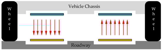
Figure 9.
The four-plate parallel structure in the large air gap mode.
In the four-plate vertical structure, as shown in Figure 10, two transmitter plates are vertically stacked in different planes at the road surface, where the area of the lower plate is slightly larger than that of the upper plate [41]. Two receiver plates are placed in the same way at the EV chassis, where the upper plate’s area is slightly larger than the lower plate’s. The two pole plates with slightly larger areas above the chassis and below the ground play power transfer roles and the two pole plates with slightly smaller areas below the chassis and above the road play power return roles [47,48]. The advantage of this scheme is that the area at the chassis is saved, and the electric field dissipation is reduced. Still, the capacitive interference between the vertical structure of each pole plate is significant, and the decoupling calculation is required, which reduces the capacitance utilization of the pole plate. In addition, the distance between the pole plates on the same side is reduced, which puts higher requirements on the insulation between the pole plates.
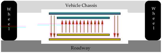
Figure 10.
The four-plate vertical structure in the large air gap mode.
Based on the four-pole-plate vertical coupling mechanism, the two-plate vertical structure is formed by using the parasitic capacitance between the vehicle chassis and the roadway as a power circuit [49,50], as shown in Figure 11. Since only two pole plates are used as the coupling mechanism, this scheme reduces the overall cost of the coupling mechanism. Since the parasitic capacitance is used as the power transmission path, there is no need to analyze the parasitic capacitance influence for subsequent decoupling analysis [51]. However, compared with the coupling capacitance formed by using metal pole plates, the parasitic capacitance is more challenging to control because its value is more dependent on factors such as ground and chassis flatness, while the current flowing through the roadway will generate more significant losses and impact the power of the system.
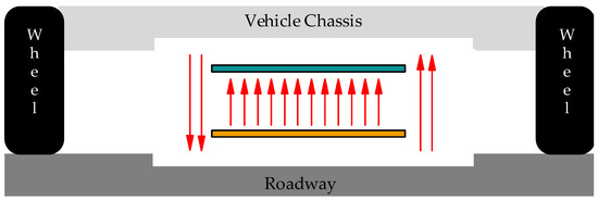
Figure 11.
The two-plate vertical structure in the large air gap mode.
3.2.2. Equivalent Capacitance Mode Using EV’s Body Structure
Using the body structure to form the equivalent capacitance means that the material with a high relative dielectric constant is selected as the medium according to the different material compositions of different parts of the EV, and the equivalent capacitance is formed by coupling mechanism attachment. It differs from the large-area and long-distance pole plate mode of the “equivalent capacitance mode using large air gap” by having a shorter power transmission distance and a higher relative dielectric constant in the medium between pole plates. Therefore, the coupling plates do not necessarily have to be significant in size to achieve the required coupling capacitance values. Currently, the EV’s body structure provides three modes for equivalent capacitance:
- Equivalent capacitance using the windows;
- Equivalent capacitance using the body coating;
- Equivalent capacitance using the wheels.
Figure 12 shows each mode’s schematic diagram and the relative dielectric constant.

Figure 12.
Composition and relative dielectric constants of different parts of the EV body.
An EV window was used by a research team from Daegu University in 2016 to generate an eight nF coupling capacitance using a coupling pole plate with an area of 2400 cm2 and 2-mm-thick glass as a medium [52]. Following the research, in 2017 the research team at Daegu University proposed using an Indium Tin Oxide (ITO) transparent conductor instead of a conventional copper plate as a vehicle coupling pole plate [53], as shown in Figure 13. Consequently, the pole plate had better light transmission, so it did not have to be removed in a non-charging state to ensure light transmission in the vehicle. The advantage of using the window as the coupling medium is that it has a large surface area and is placed on the vehicle’s surface, making it easy to lay the coupling pole plate. It does not require any structural changes. However, during the charging process, there is a risk of scratching the window glass. At the same time, the transparent conductor ITO is carcinogenic to the human body, which limits its application.
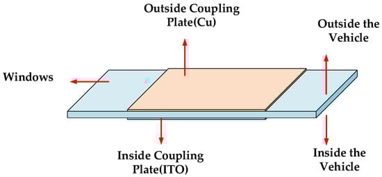
Figure 13.
Using the window as the coupling medium.
EV body insulation coatings include under coatings (which consist primarily of epoxy resin), intermediate coatings (which consist primarily of polyester), and top coatings (which consist primarily of polyurethane). In 2021, a research team at Utsunomiya University proposed using a body insulation coating as a coupling medium, attaching a metal plate inside the body as a power receiver, and attaching a metal pole plate at the hood and doors outside the vehicle as a power transmitter for power transfer, as shown in Figure 14. This equivalent capacitance of 20.6 nF was fabricated with a 250 mm × 250 mm coupling pole plate under an insulation coating with an additional 110 mm thickness [54].
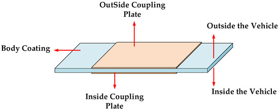
Figure 14.
Using the body insulation coating as a coupling medium.
Because the insulation coating is relatively thin, the distance between the coupling poles of a solution using the insulation coating as the medium is relatively small, resulting in an enormous coupling capacitance value. However, because the insulation coating is often exposed to the external environment, under the influence of wind, snow, sand, high and low temperature, and other complex climates, the composition and thickness of the body insulation coating will change, resulting in the capacitance value of the coupling mechanism shifting to cause system detuning, affecting the stability of its application.
In 2011, a research team from Toyohashi University of Science and Technology proposed a power transfer scheme using wheels as a medium, placing power receiver plates on the inner layer of the wheels, and placing power transmitter plates within the roadway [34,55,56], as shown in Figure 15, and in 2013 conducted experiments on a small electric toy car [35]. In 2016, the team modified the small EV wheel structure by embedding a power receiver pole plate at the car wheel and a power transmitter pole plate in the asphalt roadway to achieve 900 W power transmission [38,57]. The system also had a certain dynamic power transfer ability and could travel a distance of 4 m at a speed of 10 km/h [38].
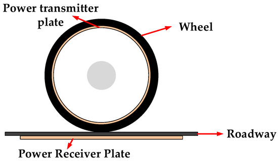
Figure 15.
Using the wheels as a coupling medium.
With wheels as the medium, charging is more effortless since the vehicle only needs to be parked at the designated location, and no external machine is required. Despite this, burying the pole plate in the roadway makes it difficult to perform future maintenance and repair operations, and the coupling mechanism placement requires structural modifications to the roadway and vehicle wheels.
3.2.3. Capacitive Patterns Are Formed by Attaching the Coupling Mechanism to the Body Surface
The coupling mechanism attached to the body surface of the EV to form the mode refers to the scheme of power transfer by placing the power receiver pole plate on the body surface and coupling it with the external power transmitter pole plate. It only requires the installation of a pole plate on the body to transmit power, not modification of the body structure. Moreover, the flexible structure enables the external transmitter pole plate to be tightly attached to the body, reducing power transfer distance and electric field dissipation, thereby allowing the coupling pole plate to be coupled with a sizeable equivalent capacitance without using a large area, as shown in Figure 16.
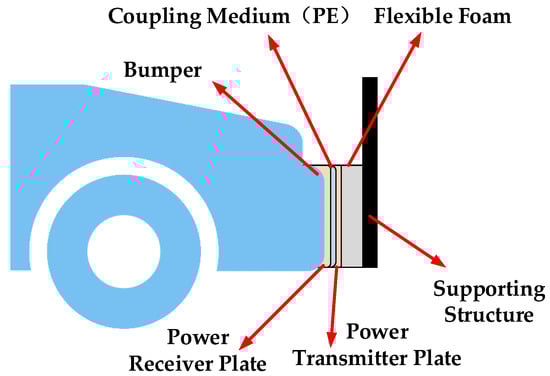
Figure 16.
Attaching the coupling mechanism to the body surface to form a coupling mechanism.
In 2015, a research team at the University of Wisconsin–Madison placed the receiver pole plate at the bumper of an EV, made a power transmitter pole plate with metal foil, and installed it at the transmitter mechanism with a 0.1 mm thick layer of PE material located on the surface of the metal foil as the coupling medium, and generated an equal coupling capacitance of 10 nF with only a 0.1 m2 area of the coupling pole plate [36,58].
The coupling mechanism was attached to the body surface to form the capacitance mode without modifying the structure of the EV itself, and the charging process would not damage the EV’s shell, so it would be easy to repair and replace the coupling mechanism, with low installation costs and easy maintenance. However, the coupling mechanism on the EV’s surface affects its aesthetics, and it would be easily damaged if the vehicle is scratched.
A comparison of the characteristics of the coupling mechanism placement methods in different static power transfer scenarios is shown in Table 2, where the coupling capacitance is discounted by in the T/-type equivalent model or in the single-capacitance equivalent model.
Table 2.
A comparison of the characteristics of the coupling mechanism placement modes in different static power transfer scenarios.
The relationship between the coupling capacitance value and the coupling pole plate area, as well as the transmission distance between the pole plates under different coupling mechanism placement modes, is shown in Figure 17.
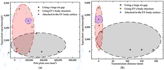
Figure 17.
Relationship between different modes of coupling capacitance and pole plate area as well as power transfer distance: (a) relationship between coupling capacitance and pole plate area for different modes; (b) relationship between different modes of coupling capacitance and power transmission distance.
3.3. Coupling Mechanism Placement in Dynamic Power Transfer Scenarios
The technology of dynamic power transfer allows EVs to be powered while driving. An EV in dynamic power transfer technology is a moving body instead of a static one in static power transfer technology. To ensure power transfer continuity, the coupling mechanism, particularly the transmitter end of the coupling mechanism, needs to be reasonably designed so that the built-in coupling pole plate of the EV can maintain a relatively stable equal coupling capacitance with the power transmitter pole plate during the moving process.
The existing technology of CPT for EV wireless power transfer can roughly be divided into two categories: long-rail and segmented.
Long-rail type power transfer systems extend the power transmitter from the conventional coupling pole plate directly opposite the receiver to a larger area and more extensive rail. When the power receiver pole plate moves within the range of the rail, the coupling area remains constant, so the capacitance remains constant.
3.3.1. Conventional Parallel Long Rail Power Transfer
The conventional parallel long rail-type structure can be divided into three structures depending on the position of its pole plate.
In structure 1, the power transmitter pole plate is placed horizontally along the road, and the power receiver pole plate placed at the vehicle’s chassis is coupled with the power transmitter pole plate in the road, as shown in Figure 18 [60,61]. It is easy to install receiver pole plates and transmitter pole plates in this structure, and the vehicle requirements and road requirements are low. However, due to the large air gap between the vehicle’s chassis and the roadway, the power transmission distance is large, resulting in a small coupling capacitance and large dissipation of the electric field.
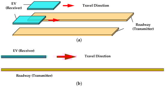
Figure 18.
Structure 1 of conventional parallel long rail power transfer: (a) stereogram; (b) front view.
In structure 2, two transmitters are fixed vertically on the road, and two receivers are fixed vertically on the vehicle chassis between the transmitters, as shown in Figure 19 [61]. For this structure, the receiver and transmitter poles do not need a large air gap. In contrast, the outer transmitter pole plate can form a certain shielding effect, so its equal coupling mutual-capacitance value is more significant, and the electric field dissipation is more negligible. Nevertheless, this structure has poor applicability, the coupling pole plate placement is complex, and the power transmitter plate needs to be laid vertically to the road surface.

Figure 19.
Structure 2 of conventional parallel long rail power transfer: (a) stereogram; (b) top view.
In structure 3, two transmitters are fixed vertically on the road, and two receivers are fixed vertically on the vehicle chassis outside the transmitters, as shown in Figure 20 [61]. Under this structure, the same side of the receiver and transmitter plates also do not need a large air gap between them. In contrast, the distance between the two groups of transmitter plates and between the two groups of receiver plates are both farther, and the transmitter plates between the two groups of receiver plates form a metal shield [62]. Therefore, their equal coupling mutual-capacitance is larger, the parasitic capacitance between the plates is smaller, and the coupling coefficient is higher. However, this structure is limited by significant electric field dissipation, high coupling pole plate requirements, and poor applicability and is almost exclusively applicable to electrified rail locomotives.
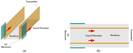
Figure 20.
Structure 3 of conventional parallel long rail power transfer: (a) stereogram; (b) top view.
It is worth noting that in Structure 1 the distance between the power transmitter plate and the receiver plate is large due to the air gap between the vehicle chassis and the roadway. In Structures 2 and 3, there is no structural limitation between the power transmitter and receiver plates. The power transmission distance can be shortened by adjusting the plate’s position.
3.3.2. Strip-Coupler Long Rail Power Transfer
In order to further reduce the cost while enhancing the system resistance to offset and reduce the electric field dissipation effect, a research team from Jilin University proposed the strip-coupler long rail power transfer system in 2019, as shown in Figure 21. Based on the conventional parallel long rail power transfer system, the power transmitter end is shrunk into a circular cable with a radius of 5 mm. This way, the power transmitter rail material consumption can be significantly reduced, and the amount of aluminum required can be reduced to 0.0785 m3/km, only 3.2% of the original amount. Additionally, the strip-coupler is smaller than conventional parallel long rails, making installation easier. Further, since the size of the power transmitter plate is smaller than the power receiver plate at the vehicle, the equivalent capacitance can be kept constant as long as the power transmitter plate is kept in the range of the power receiver plate so that the EV has a certain degree of freedom of lateral movement and reduces electric field dissipation [63]. Compared with the conventional parallel long rail, the disadvantage is that this structure has a considerably smaller frontal area, decreasing its equivalent capacitance value, making it more challenging to achieve high-power transfer.
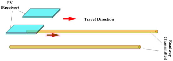
Figure 21.
Strip-coupler long rail power transfer.
3.3.3. Wheeled Long Rail Power Transfer
In order to reduce power transmission distance, increase equal coupling capacitance, and reduce electric field dissipation during power transmission, the wheeled long-rail power transfer system was proposed in 2016 by Naoki Sakai’s research team at Toyohashi University of Science and Technology, as shown in Figure 22. The coupling mechanism on the receiver side was placed in the vehicle wheel and coupled to the long rail transmitter plate at the roadway. As a result, the power transfer distance of the structure was reduced, the equal coupling capacitance was increased, and the electric field dissipation was reduced. Through this power transfer structure, the team transferred 1 kW with an efficiency of 80.2% [57], enabling the EV to travel a distance of 4 m at 10 km/h [38]. However, this structure is more complex than the conventional parallel long rail structure because it requires modification of the vehicle wheels.
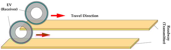
Figure 22.
Wheeled long rail power transfer.
3.3.4. Vertical Long Rail Power Transfer
To reduce the size of the coupling mechanism, Siqi Li’s research team at Kunming University of Science and Technology proposed the vertical long rail dynamic coupling mechanism in 2016 [64], as shown in Figure 23. The power receiver pole plate on the EV side and the power transmitter pole plate on the road surface were in vertical placement. Placing the coupling pole plate vertically reduced the coupling pole plate volume, enhancing the self-coupling capacitance value. However, due to the distance and presence of metal shields on the power return side of this structure, the return measurement mutual-capacitance value was tiny, affecting the power transmission. A solution to the mutual-capacitance problem on the return side of the Vertical long rail structure can be found in the literature [64,65] by combining the actual structure of railroad electric locomotives in order to electrically connect the metal wheels to the chassis, which in turn provides a way for power to be returned, which overcomes the problem of small return measurement mutual-capacitance.

Figure 23.
Vertical long rail power transfer.
3.3.5. Segmented Power Transfer
Unlike the long rail structure described above, in the segmented wireless power transfer system, power transmitters are segmented into different groups to form the overall power transmitter, and each group of power transmitters is equipped with its inverter source. When the vehicle drives over the power transmitter segment, the power receiver at the vehicle receives power, and when the vehicle moves, the receiver takes power from the different power transmitter segments [27,66,67,68], as shown in Figure 24.
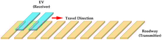
Figure 24.
Segmented power transfer.
Compared with the long rail structure, the segmented type can transfer power to multiple EVs simultaneously, reducing electric field dissipation and enhancing power efficiency [68,69]. However, the structure control system is complex, and more switching power supplies are required at the transmitter end, increasing costs. Additionally, equal coupling capacitance fluctuates as the vehicle travels through different transmission segments, causing a certain pulsation of power transmission, which can damage the battery.
A comparison of the characteristics of different dynamic power transfer structures is shown in Table 3.
Table 3.
A comparison of the characteristics of different dynamic power transfer structures.
4. Resonance Compensation Networks
4.1. Requirements of EV Wireless Power Transfer for Resonance Compensation Network of CPT System
As an essential part of the CPT system, the resonance compensation network plays a role in regulating the voltage quality, boosting the voltage at both ends of the pole plate, and reducing the sensitivity of the system parameters [25,71,72]. Compared to conventional CPT systems, CPT resonance compensation networks adapted to EV wireless power transfer systems require the following characteristics: Firstly, the transfer power of the CPT system of EV is higher than that of the conventional CPT system. As power increases, the voltage stress on each component in the resonance compensation network increases, requiring the resonance compensation network to have a particular voltage-dividing capability to prevent electric breakdowns. Secondly, it is required that when the system power increases, the system efficiency also increases, which makes it necessary for the output power of the resonance compensation network to be positively correlated with the coupling coefficient [48]. Finally, to ensure power output stability, the resonance compensation network must have load-independent constant voltage or constant current capability.
4.2. Constant-Current Output Type Resonance Compensation Network
In the resonance compensation network of the CPT system applicable to EV wireless power transfer, the resonance compensation networks that can achieve load-independent constant current output are double-sided LCL type, double-sided LCLC type, double-sided CLLC type, and EFR type, and the output currents (i.e., output power) of all four types of resonance compensation networks are positively related to the coupling coefficient.
The double-sided LCL-resonance compensation is shown in Figure 25, where the power transmitter side consists of two inductor devices, and , and a capacitor device, , and the power receiver side consists of two inductor devices, and , and a capacitor device, [41]. The topology network can be regarded as a superposition of the primary and secondary T-type LCL topology with a low-order SS-type compensation inductor and a coupling mechanism [73].
Figure 25.
The double-sided LCL-resonance compensation: (a) topology of the coupling mechanism after equating with the -type equivalent model; (b) schematic diagram of the network structure; (c) resonance working relationship diagram.
The topology of the system is shown in Figure 25, and the coupling coefficient, , is defined as . When the system operates at the resonance frequency, the primary inductor, , and the primary capacitor, , form a resonance. Similarly, the secondary inductor, , and the secondary capacitor, , form a resonance, as shown in Equation (7). The primary inductor, , with capacitor and , and form a resonance, and similarly, the secondary inductor, , with capacitor and , and form a resonance, as shown in Equation (8) [74].
The network can achieve load-independent constant-current output under the condition of Equations (7) and (8), which is the ZPA (Zero Phase Angle) state, and the output current calculation equation is shown as Equation (9).
The coupling pole plate can form a high voltage to meet the requirements of high-power scenarios after boosting the T-type LCL structure. However, because there is no compensation capacitor at the port of the coupling mechanism, to maintain the resonance inductance volume within a reasonable range, it is often necessary for the coupling mechanism to have a large self-capacitance [41], making it more suitable for vertical coupling mechanisms or coupling mechanisms with large self-capacitances.
The double-sided LCLC-resonance compensation network is shown in Figure 26. Based on the double-sided LCL topology, a pair of compensation capacitors, and , are connected in parallel at the ports of the coupling mechanism [37,43]. This topology network can be regarded as a superposition of the primary and secondary T-type LCL topology with a low-order SS-type compensation inductor and a coupling mechanism with compensation capacitors [73].
Figure 26.
The double-sided LCLC-resonance compensation: (a) topology of the coupling mechanism after equating with the -type equivalent model; (b) schematic diagram of the network structure; (c) resonance working relationship diagram.
The topological resonance relationship of the double-sided LCLC type is similar to the double-sided LCL type, and the only difference is that after the connection of the external compensation capacitor, the primary and secondary self-capacitance capacitance, and , become the superposition of the coupling mechanism self-capacitance and external compensation capacitance, that is, , and the coupling coefficient, , is defined as when the system operates at the resonance frequency; the resonance relationship between and and and is shown in Equation (7). The primary inductor, , with capacitor and , and form a resonance, and similarly, the secondary inductor, , with capacitor and , and form a resonance, as shown in Equation (10).
The network can achieve load-independent constant-current output when the conditions of Equations (7) and (10) are satisfied, and the output current and calculation equation are shown in Equation (11) [75].
The double-sided LCLC topology effectively increases the value of parallel port capacitance with the addition of compensation capacitors, which can reduce the volume of the resonance inductor and is suitable for both parallel and vertical coupling mechanisms.
The double-sided CLLC-resonance compensation is shown in Figure 27, where the power transmitter consists of two inductor devices, and , and two capacitor devices, and . The power receiver consists of two inductor devices, and , and two capacitor devices, and . This topology network can be regarded as a superposition of the primary and secondary T-type CLC topology with a low-order SS-type compensation inductor and a coupling mechanism with compensation capacitors [73].
Figure 27.
The double-sided CLLC-resonance compensation: (a) topology of the coupling mechanism after equating with the -type equivalent model; (b) schematic diagram of the network structure; (c) resonance working relationship diagram.
When the system operates at the resonance frequency, the double-sided CLLC- resonance compensation network has the same element resonance relationship as the double-sided LCLC-resonance compensation network, as shown in Equations (7) and (10).
The network can achieve load-independent constant-current output when the conditions of Equations (7) and (10) are satisfied; the output current calculation equation is also the same as the double-sided LCLC-resonance compensation network, as shown in Equation (11).
The double-sided CLLC type topology network can not only satisfy the high power requirement but also, compared with double-sided LCL and double-sided LCLC topology networks, the resonance inductance of the primary and secondary sides are smaller and easier to achieve under the condition of achieving the same output [46].
The EFR resonance compensation is shown in Figure 28, where the power transmitter side consists of two inductor devices, and , and two capacitor devices, and , with a mutual-inductance value of between the two resonance inductors, and the receiver side consists of two inductor devices, and , and two capacitor devices, and , with a mutual-inductance value of between the two resonance inductors [76]. This topology can be regarded as a superposition of the primary and secondary M-type mutual inductance topology and a coupling mechanism with compensation capacitors [73].
Figure 28.
The EFR resonance compensation: (a) topology of the coupling mechanism after equating with the -type equivalent model; (b) schematic diagram of the network structure; (c) resonance working relationship diagram.
When the system operates at the resonant frequency, the EFR resonance compensation has the same element resonance relationship as the doubled-sided LCLC-resonance compensation network (and the doubled-sided CLLC-resonance compensation network), as shown in Equations (7) and (10).
The network can achieve load-independent constant-current output when the conditions of Equations (7) and (10) are satisfied, and the output current and calculation equation are shown in Equation (12).
Mutual-inductance between the two inductors of the EFR-type compensation structure adds new circuit parameters, which allows more freedom in designing the system circuit parameters and facilitates adjusting system performance [77,78].
4.3. Constant-Voltage Output Type Resonance Compensation Network
In the resonance compensation network of the CPT system applicable to EV wireless power transfer, the resonance compensation networks that can achieve load-independent constant voltage output are CLLC-CL type, LCL-L type, LCLC-CL type, and M-SS type, and the output voltage (i.e., output power) of all four types of resonance compensation networks are positively related to the coupling coefficient.
The LCL-L-resonance compensation is shown in Figure 29, where the transmitter side consists of two inductor devices, and , and a capacitor device, . The receiver side consists of an inductor device, [48]. The topology network can be regarded as a superposition of the primary T-type LCL structure with a low-order SS-type compensation inductor and a coupling mechanism.
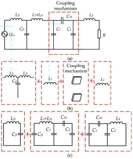
Figure 29.
The LCL-L-resonance compensation: (a) topology of the coupling mechanism after equating with the -type equivalent model; (b) schematic diagram of the network structure; (c) resonance working relationship diagram.
When the system operates at the resonance frequency, the primary inductor, , and the primary capacitor, , form a resonance, as shown in Equation (13). The remaining elements have the same resonance relationships as the double-sided LCL-resonance compensation network, as shown in Equation (8).
The network can achieve load-independent constant-voltage output when the conditions of Equations (8) and (13) are satisfied; and the output voltage and calculation equation are shown in Equation (14).
The LCL-L type topology has only three resonance elements at the transmitter side and one resonance element at the receiver side, resulting in low cost and small system size [48]. However, because there is no compensation capacitor at the port of the coupling mechanism, to maintain the resonance inductance volume within a reasonable range, it is often necessary for the coupling mechanism to have a large self-capacitance, making it more suitable for vertical coupling mechanisms or coupling mechanisms with large self-capacitance.
The LCLC-CL type topology is similar to the LCL-L type, and the only difference is that after the connection of the external compensation capacitor, the primary and secondary self-capacitance, and , become the superposition of the coupling mechanism self-capacitance and external compensation capacitance, that is, , , as shown in Figure 30 [73].
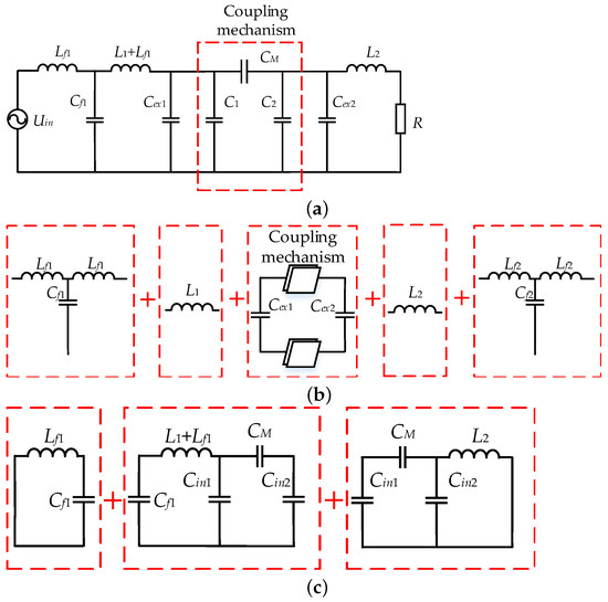
Figure 30.
The LCLC-CL-resonance compensation: (a) topology of the coupling mechanism after equating with the -type equivalent model; (b) schematic diagram of the network structure; (c) resonance working relationship diagram.
When the system operates at the resonance frequency, the element resonance relationships of the LCLC-CL type topology are similar to those of the LCL-L type topology; the only difference is that after the connection of the compensation capacitors, the self-capacitance values of the primary and secondary networks become and . The resonance relationships of the LCLC-CL type topology for each elements are shown in Equations (10) and (13) [79].
The network can achieve load-independent constant-voltage output when the conditions of Equations (10) and (13) are satisfied, and the output voltage and calculation equation are shown in Equation (15).
The LCLC-CL topology effectively increases the value of parallel port capacitance with the addition of compensation capacitors, which can reduce the volume of the resonance inductor and is suitable for both parallel and vertical coupling mechanisms.
The CLLC-CL-resonance compensation is shown in Figure 31, where the power transmitter side consists of two inductor devices, and , and two capacitor devices, and , and the power receiver side consists of one inductor device, , and one capacitor device, [62]. This topology network can be regarded as a superposition of a primary T-type CLC structure with a low-order SS-type compensation inductor and a coupling mechanism with compensation capacitors.
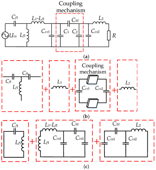
Figure 31.
The CLLC-CL-resonance compensation: (a) topology of the coupling mechanism after equating with the -type equivalent model; (b) schematic diagram of the network structure; (c) resonance working relationship diagram.
When the system operates at the resonance frequency, the CLLC-CL type topology has the same element resonance relationship as the LCLC-CL type topology, as shown in Equations (10) and (13) [80].
The network can achieve load-independent constant-voltage output when the conditions of Equations (10) and (13) are satisfied, and the output voltage and calculation equation are shown in Equation (15).
Compared with the LCLC-CL structure, the primary resonance inductor, , is smaller and easier to achieve under the condition of achieving the same output [81].
The M-SS type compensation network is shown in Figure 32, where the power transmitter side consists of two inductor devices, and , and two capacitor devices, and , with a mutual-inductance value, , between the two resonance inductors [82], and the receiver side consists of one inductor device, , and one capacitor device, .
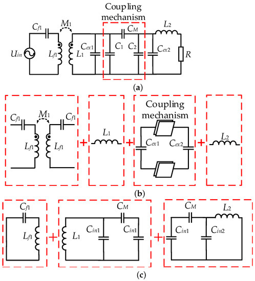
Figure 32.
The M-SS type compensation network: (a) topology of the coupling mechanism after equating with the -type equivalent model; (b) schematic diagram of the network structure; (c) resonance working relationship diagram.
When the system operates at the resonance frequency, the M-SS type compensation network has the same element resonance relationship as the LCLC-CL type topology (and the CLLC-CL type topology) [82], as shown in Equations (10) and (13).
The network can achieve load-independent constant-voltage output when the conditions of Equations (10) and (13) are satisfied, and the output voltage and calculation equation are shown in Equation (16).
Similar to the EFR-type compensation network, the mutual-inductance between the two inductors of the M-SS type compensation network adds new circuit parameters, which allows more freedom in designing the system circuit parameters and facilitates adjusting system performance.
A summary of high-power CPT resonance compensation networks adapted to EV wireless power transfer scenarios is shown in Table 4, where the coupling capacitance is discounted by in the T/-type equal network or in the single-capacitor equal network.
Table 4.
A summary of high-power CPT resonance compensation networks adapted to EV wireless power transfer scenarios.
5. Directions for the Development
Although CPT technology has already achieved a series of results in the field of EV wireless power transfer, it still has many shortcomings compared with IPT technology. In order to achieve further development of CPT technology, it can be developed in three directions: high-power transmission, high-efficiency transmission, and high-security transmission.
5.1. High-Power Transmission
The low power level of existing CPT power transfer systems compared to the wire-conducted power supply and IPT wireless power transfer is a prominent factor limiting the application of CPT technology in EVs. Upgrading the power of CPT systems can be carried out by three technical routes: adopting higher-order resonance compensation networks, using multiple-input systems, and upgrading component withstand voltage values.
5.1.1. Adopting Higher-Order Resonance Compensation Networks
Early CPT systems were mainly based on single inductor compensation, due to the single compensation system, so the early CPT system transmission power is generally only a few tens of watts [86,87,88,89]; with the development of low-order compensation systems represented by double-sided LC-type resonance compensation networks, the power level of CPT was raised to the hundred-watt level [90,91,92,93]. After introducing higher-order networks represented by double-sided LCLC-type resonance compensation networks, the power level of CPT systems was raised to values above 2 kW. It can be seen that the development of high-order resonance compensation networks is a crucial way to enhance the power level of CPT systems and an effective means to further develop CPT technology in high-power scenarios.
5.1.2. Using Multiple-Input Systems
The power limitations of a single CPT system can be overcome by connecting multiple-input systems in parallel for power input. This is called “multiple-input, single-output” mode. Multiple parallel inputs include multiple parallel inverters and multiple parallel transmitter channels.
Multiple parallel inverter input means that multiple inverters are connected in parallel at the power transmitter for power input. The parallel structure of multiple inverters can significantly reduce the current stress of the switching devices and thus increase the system input power. Due to timing and component tolerance-related mismatches and high-frequency circuit parasites, paralleling high-frequency inverters directly can bring the challenge of uneven current sharing and circulating currents. To solve these challenges, a research team at Cornell University proposed four power combination architectures: in-phase power combiner, out-phased power combiner, quadrature power combiner, and immittance network-based power combiner, which can realize parallel power input and then enhance the power level, as shown in Figure 33. Eventually, the immittance network-based power combiner connects two power structures in parallel. It produces 2.3 kW of output power at 6.78 MHz with almost half the current stress per switching tube compared to a conventional single-inverter CPT system [94].
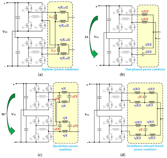
Figure 33.
Four multiple parallel inverter input structures: (a) Inphase power combiner; (b) out-phased power combiner; (c) quadrature power combiner; (d) immittance network-based power combiner.
Multiple parallel transmitter input means adding one or more power transmitter plates to the original CPT system. Different inverter power supplies control the additional power transmitter plates, thus increasing the number of power transmission channels. The multiple power transmission channels are added up to achieve high power transmission. Compared with multiple parallel inverter structures, the structure of multiple parallel transmitter inputs does not require the additional design of power combination architecture, and the system circuit part is simple. However, it increases the number of coupling pole plates at the transmitter side. It produces additional parasitic capacitance, which requires decoupling calculation and increases the complexity of the coupling mechanism part. In 2019, Rui-Kun Mai’s research team at Southwest Jiaotong University connected two transmitters in parallel to achieve a dual-transmitting terminal system with a power output of 1.47 kW and an efficiency of 90.63%, resulting in a 50% reduction in the current flowing through the switching tubes compared to conventional systems with the same power output [95], as shown in Figure 34.
Figure 34.
Multiple parallel transmitter input.
5.1.3. Upgrading Component Withstand Voltage Values
The voltage stress of each component in the system increases as the power increases, resulting in component damage as the voltage stress exceeds the component voltage stress tolerance value. Therefore, component voltage withstand capability is one of the critical factors limiting the power increase of the CPT systems. In CPT systems, parallel with coupling mechanisms, compensation capacitors are often subjected to the highest voltage stress, up to thousands of volts. For this reason, improving withstand voltage of the compensation capacitors is fundamental to improving the withstand voltage of the components.
Using vertical coupling mechanism or another coupling mechanism with a larger self-capacitance is crucial to solving the compensation capacitance withstand voltage problem. Without any external capacitor, only the coupling mechanism itself can provide the compensation capacitance required by the system. After corresponding insulation measures are taken, the coupling mechanism is capable of withstanding the voltage itself, thus solving the voltage resistance issue. Using capacitor components with higher withstand voltage performance is a technical way to withstand voltage stress, and the different capacitor devices have different voltage withstand levels, as shown in Table 5 [96,97]. Components with higher voltage and current withstand values, especially capacitor devices, must be developed in conjunction with new material technologies, structures, and other fields. This is also an effective solution to enhance the power level of CPT systems.
Table 5.
Different voltage withstand levels of different capacitor devices.
Using a series-parallel connection of components is also an essential solution to the problem of components withstanding voltage. The component group’s overall voltage and current withstand capability can be enhanced under the condition that the components’ overall capacitance and inductance value remain unchanged after connection to meet the actual requirements of high-power scenarios.
5.2. High-Efficiency Transmission
In the existing research of EV wireless power transfer, the efficiency of CPT technology still has more improvement space compared with IPT technology [71]. There are three leading causes of efficiency loss in CPT systems: loss of inverter and rectifier parts, loss of coupling mechanism, and loss of resonance component.
5.2.1. Reducing the Loss of Inverter and Rectifier Components
The loss of inverter and rectifier devices can be divided into conduction loss and switching loss. The conduction loss refers to the power loss caused by the on-resistance of the switching device when the current flows through the switching device of the inverter rectifier, and the switching loss refers to the power loss caused by the voltage and current of the switching device that cannot be changed suddenly and then interleaved during the process of opening and closing the switching device [77]. Using new-generation semiconductor devices and designing circuits with soft switching states can reduce the losses of inverters and rectifiers [98].
New-generation semiconductor devices are represented by silicon carbide (SiC) and gallium nitride (GaN), and their characteristics compared with traditional silicon-based devices are shown in Table 6 [99].
Table 6.
New-generation semiconductor devices are represented by silicon carbide (SiC) and gallium nitride (GaN), and their characteristics are compared with traditional silicon-based devices.
According to Table 6, SiC/GaN has a critical breakdown electric field more than ten times higher than silicon, Si, which significantly increases the current density and voltage withstand capacity of these two semiconductor power devices and significantly reduces the conduction loss as well. Additionally, SiC/GaN’s saturation velocity is twice that of silicon, Si, making it more suitable for CPT systems due to its high-frequency characteristics. A comparison of the conversion efficiency of switching power supplies using SiC/GaN devices with Si devices is given in the literature [99]. The efficiency of the inverter rectifier is improved using SiC/GaN power devices, as shown in Figure 35.
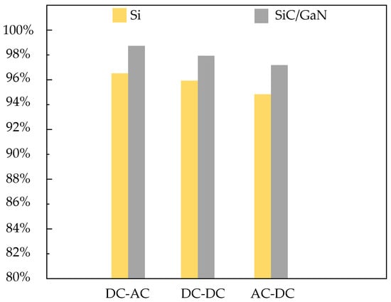
Figure 35.
Comparison of the efficiency of SiC/GaN devices with conventional Si devices in the power conversion process.
Despite being part of the same new generation of wide-band semiconductor devices, GaN and SiC differ in their material properties and device structure, thus resulting in different output power, voltage levels, and performance capabilities, leading to different application scenarios for each device [100]. From an electrical perspective, GaN switching losses at low to medium voltages (below 1200 V) are approximately three times lower than SiC at 650 V. Additionally, GaN devices have better performance at frequencies over 500 kHz, whereas SiC is usually designed to operate at voltages of 650 V, 1200 V, and more; SiC devices are more suitable for working in hot and harsh environments due to their high junction temperature characteristics [100,101].
Class D and Class E converters easily achieve soft switching and high power conversion efficiency among the commonly used CPT inverter circuits [102,103]. However, they are prone to high-voltage stress and sensitive to changes in component parameters, making them unsuitable for EVs with high power demands [103]. For full-bridge inverters that can operate at high power, soft switching can be achieved by operating the circuit in the inductive region. In the literature [77], by adjusting the values of the system resonance element parameters, the system as a whole is made to be weakly inductive, thereby enabling the system to operate in a soft switching state, reducing switching losses and increasing the efficiency to 95% at a system output of 3.2 kW.
5.2.2. Reducing the Loss of the Coupling Mechanism
The coupling mechanism is also one of the primary sources of power loss in the CPT system. In EV wireless power transfer CPT systems, the power loss of the coupling mechanism mainly occurs due to the parasitic resistance of the coupling pole plate and the parasitic capacitance between the coupling mechanism and the external environment, such as the vehicle chassis and the roadway.
The coupling pole plate parasitic resistance is shown schematically in Figure 36, and its calculation equation is shown in Equation (17) [14]. When the current flows through, it generates a loss of in the parasitic resistance. Where I is the current flowing through the coupling mechanism and is the coupling mechanism parasitic resistance.
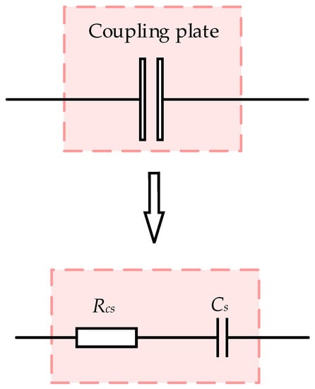
Figure 36.
Schematic diagram of parasitic resistance of coupling mechanism.
In Equation (17), is the loss angle tangent value , expressed as the residual angle resulting from the phase angle between the phase current flowing within the medium and the phase voltage when an AC voltage is applied.
is the operating angular frequency of the system. is the equal capacitance of the coupling pole plate, and its calculation equation is shown in Equation (6).
As can be seen from Equations (6) and (17), raising the system’s operating frequency reduces the parasitic resistance of the coupling pole plate. Additionally, the loss angle tangent value of the coupling plate is positively correlated with its relative dielectric constant, i.e., increasing the relative dielectric constant of the coupling plate increases the equal inter-pole capacitance of the coupling plate, but at the same time increases its loss angle tangent value. To reduce the parasitic resistance of the coupling plate, it is important to select the coupling plate interpolar medium with a balance between its relative dielectric constant value and its loss angle tangent value. Let be the ratio of the loss angle tangent to the relative dielectric constant, i.e., .
Then the parasitic resistance of the coupling mechanism can be expressed in the form of Equation (18).
Equation (18) shows that the parasitic resistance of the coupling mechanism is only positively proportional to when the distance between the poles of the coupling plate and the orthogonal area is constant. The relative dielectric constant and the loss angle tangent values of common substances and are shown in Table 7 [104,105].
Table 7.
The relative dielectric constant and the loss angle tangent values of common substances and .
In the EV wireless power transfer scenario, a series of parasitic capacitances are generated in addition to the coupling capacitance between the power transmitter side of the coupled pole plate and the power receiver. These parasitic capacitances originate from cross-coupling between the plates , as well as from coupling between two plates on the same side ( and , the plates and the roadway ( and , the plates and the vehicle chassis and , the roadway and the vehicle chassis , the roadway and the inverter ground , and the vehicle chassis and the rectifier ground , as shown in Figure 37 and Table 8.
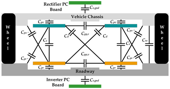
Figure 37.
Schematic diagram of parasitic capacitance of EV coupling mechanism.
Table 8.
A series of parasitic capacitances.
In the case of parasitic capacitances, when the current passes through them, the power transfer is reduced, resulting in lower system efficiency [67,106,107,108].
To resolve the parasitic capacitance problem, in 2019, a research team at Cornell University used a separated inductor matching network. An inductor in a matching network was divided symmetrically into two halves, with one half placed in the forward path and the other in the return path. As a result, power loss was minimized by avoiding current flow through parasitic capacitors , ground, , ground, and . Furthermore, the remaining parasitic capacitance was utilized as a compensation capacitor, which was reduced to a four-capacitance model by the decoupling method shown in Equation (19), as shown in Figure 38.
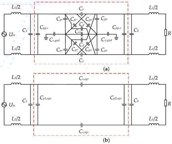
Figure 38.
Parasitic capacitance of coupling mechanism and its decoupling results; (a) equal topology of the parasitic capacitance of coupling mechanism; (b) four-capacitance model after decoupling of the parasitic capacitance of coupling mechanism.
5.2.3. Reducing the Loss of Components
Since CPT systems are usually operated at a high frequency, component losses are primarily due to inductor losses, and inductor losses frequently comprise the most considerable portion of CPT system losses. Several factors contribute to more significant power losses in conventional inductors. Due to their higher internal resistance, conventional inductor devices consume more power than other devices. Secondly, some inductors with magnetic cores also result in additional hysteresis and eddy current losses at high frequencies; furthermore, structural and material limitations can result in a lower quality factor of inductor devices, causing more significant power losses. Finally, the frequency effect of inductor devices causes the inductance of inductor devices to decrease when frequency increases, increasing power loss.
To overcome the losses in conventional inductor devices, a team of Cornell University researchers proposed new Semi-Toroidal Interleaved-Foil (STIF) coupled inductors and Toroidal Interleaved-Foil (TIF) coupled inductors in 2019 and 2022, respectively [107,108,109]. These new interleaved-foil coupled inductors have a semi-toroidal or toroidal structure, respectively, where on the outer surface of the toroidal or semi-circular structure, the parallel wires are laterally adjacent and in alternating positions, while along the inner surface, the parallel wires are stacked but also in alternating positions. This unique inductor winding is equivalent to coupling two inductors. With the two inductors coupled, the flux from one increases the flux from the other, increasing the overall inductance and reducing the wire turns for the same inductance value, thereby reducing winding losses [32,110]. Compared to conventional single-layer foil-wire coupled inductors, the AC resistance of interleaved-foil coupled inductors can be significantly reduced, as shown in Figure 39 (resonance frequency of 13.56 MHz) [32,109].
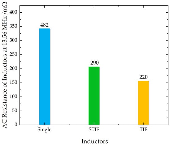
Figure 39.
AC Resistance Comparison of New Interleaved-Foil Inductors and Conventional Single-Layer Foil Wire-Coupled Inductors at 13.56 MHz Frequency.
Finally, the team transferred 320 W of power with 94% efficiency using STIF-coupled inductors and 3.75 kW with 94.7% efficiency using TIF-coupled inductors.
5.3. High-Security Transmission
5.3.1. The Security of Electric Field Dissipation
Power transmission in CPT systems involves not only the electric field power at the transmitter end flowing to the receiver end but also some of it flowing into the external environment, resulting in power dissipation. It is likely that the electric field dissipating to the outside environment will cause damage to human and electronic equipment within the vicinity. According to the standard for safety levels concerning human exposure to electric fields in IEEE C95.1-2019, the range of safety levels for the human body at high frequencies is shown in Table 9 [111,112].
Table 9.
The range of safety levels for the human body at high frequencies.
The following five options can be used to reduce electric field dissipation: low gap charging mode, adding a shielding layer, optimizing the structure and shape of the coupling pole plate itself, adjusting the coupling plate area, and utilizing segmented coupling mechanisms.
The low gap power transferring mode means that among the coupling mechanism placement modes discussed in Section 3, both modes of “equivalent capacitance mode using the EV’s body structure” and “capacitive patterns are formed by attaching the coupling mechanism to the body surface” are preferred with low transmission gaps, rather than “equivalent capacitance mode using the large air gap” with high transmission gaps. By reducing the power transfer gap, electric field dissipation is reduced. The advantage of this option is that electric field dissipation can be reduced without any additional external devices. However, in practice, not all EVs can be powered by these two modes and therefore have high requirements for use conditions.
Adding a shielding layer means adding a metal shield to the power dissipation side of the coupling mechanism. This shields the power dissipated to the external environment, thus forming a six-plate structure. As far as shielding layer material is concerned, the research team at AIUB compared the shielding performance of single metals and composite metals for the same thickness, and the average value of electric field strength under the shielding effect of a copper–zirconium–copper composite pole plate was only 49% of the average value of electric field strength under the shielding effect of pure copper pole plates at 1.5 mm thickness [113]. Adding a shielding layer option has the advantage of operating conveniently and loosening the requirements for use conditions. However, metal plates must be added as shielding layers, increasing the system’s cost and weight. Additionally, shielding layers introduce the problem of parasitic capacitance that must be decoupled for analysis, as shown in Figure 40.

Figure 40.
Structure of shield layer for coupling mechanism; (a) stereogram; (b) front view. (c) parasitic capacitance due to the addition of a shielding layer.
Adjusting the coupling plate area means reducing the area of the transmitter side of the coupling plate, similar to the “strip-coupler long rail power transfer” in Section 3.3.2. By reducing the area of the transmitter plate, the outer side of the receiver plate forms an electric field shielding effect, thereby reducing the electric field dissipation [63]. The option is easy to achieve and does not require any additional devices. Despite this, due to the reduced pole plate coupling area, the equal coupling capacitance will be further reduced, making it challenging to meet the requirements of a high-power scenario.
Optimizing the structure and shape of the coupling pole plate itself refers to the reasonable design of the structure and shape of the coupling mechanism without additional external devices to reduce the electric field dissipation. In the vertical coupling mechanism itself, the outer pole plate creates a shielding effect; therefore, under the same conditions, the electric field dissipation intensity of the system with this coupling mechanism is generally lower than that of the parallel coupling mechanism. Based on the vertical structure, the Chongqing University research team proposed a “groove” type pole plate. In this type, the shape of the outer pole plate is designed as a “groove” to form a shield, further reducing electric field dissipation [114]. The benefits of optimizing the structure and shape of the coupling pole plate itself are that no external device is needed, and no restrictions are placed on use conditions. However, the self-capacitance between the pole plates of the vertical coupling mechanism is more significant, and the utilization rate of the pole plates is lower.
Segmented coupling mechanisms divide the large coupling pole plate into several small segmented pole plates. The segmented coupling mechanism is often used in the dynamic power transfer scenario of EVs, where each small-area segmented pole plate is powered by its own separate inverter power supply, and when the phase shift between the pole plates is 180°, the edge fields between the pole plates cancel each other, thus reducing the electric field dissipation. In 2015, researchers from the University of Colorado, Boulder, used an eight-plate transmission system to transfer power at 6.78 MHz, resulting in a five-fold reduction in the electric field at the edge of the pole plate compared to a conventional two-plate design [69]. The advantage of this option is that no additional shielding mechanism is required. No structural modifications are needed to the pole plate, and the application scenario requirements are relaxed. Despite this, the segmented structure requires a separate power supply for each coupled pole plate, significantly increasing the cost of the overall system.
A comparison of the effects of different electric field dissipation reduction schemes is shown in Figure 41.
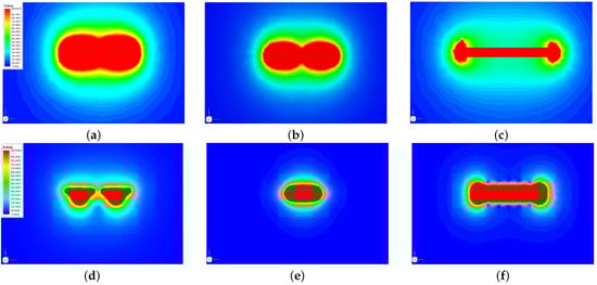
Figure 41.
Comparison of the effectiveness of different electric field dissipation inhibition schemes; (a) electric field dissipation without added electric field inhibition measures; (b) low gap power transferring solution; (c) adding a shielding layer; (d) adjusting the coupling plate area; (e) optimizing the structure and shape of the coupling pole plate itself; (f) adoption of segmented coupling mechanisms.
5.3.2. The Security High-Voltage
Considering the effects of the resonance topology of the CPT system on voltage boosting of the pole plates, voltages between the coupled plates of the CPT can reach thousands of volts or even tens of thousands of volts. Two main threats to practical EV applications are posed by high voltage. On the one hand, the high-voltage stress on the pole plate and its resonance elements damage the surroundings and the characteristics of the components. On the other hand, the high voltage generated by the pole plate and resonance element will induct a high voltage on metal objects, such as EV shells.
The most common solution for high-voltage stress on the pole plates and components is to use an insulating layer attached around the coupling pole plates and the high-voltage resonance elements. The properties of common insulating materials are shown in Table 10.
Table 10.
The properties of common insulating materials.
For the problem of high-voltage stress of resonance elements, to avoid the electric breakdown accident of resonance elements and to prolong the service life of resonance elements, a voltage optimization method of passive resonant elements is proposed in the literature [80]. Through an analysis of the relationship between the voltage stress of each resonance element and the element parameters, passive resonance element parameters are rationally configured to reduce the maximum voltage carried by the element. The compensation capacitor voltage is reduced by 17%, and the resonant inductor voltage is reduced by 15% at the same output voltage level.
For the problem of high voltage induced by the high-voltage pole plate at the metal car shell, a voltage optimization method for the EV shell voltage was proposed in the literature [115]. An analysis of the capacitance relationship between the roadway, the car shell, and the coupling mechanism was simplified to a three-capacitance model. The relationship between the car shell’s frequency and safety voltage was analyzed to optimize the resonance element parameters. Under the condition of maintaining 1.3 kW output power, the shell voltage at the periphery of the coupling mechanism was reduced to 3.88 V.
6. Conclusions
This paper analyses the potential of CPT technology in the field of EV wireless power transfer; presents a systematic review of the static and dynamic coupling mechanisms of CPT systems applicable to EV wireless power transfer; comprehensively analyses the advantages, disadvantages, and application scenarios of different coupling mechanism placements; and presents a description of the structures and characteristics of a high-performance resonance compensation network addressing the actual requirements of EV wireless power transfer. It provides a reference for the selection of coupling mechanisms and resonance compensation networks for the application of CPT system in the EV wireless power transfer field. Overall, CPT has already achieved a series of research results, but despite this, CPT technology still has many limitations when it comes to the actual application of EV wireless power transfer. Adopting high-performance resonance compensation networks, new components, and other technologies is crucial to achieving high-power and high-efficiency transmission. System structure and parameter optimization should be carried out to enhance overall system security and achieve high-security transmission so that CPT technology can be more effectively applied to the wireless charging of EVs. This will assist in laying a solid foundation for the promotion of EVs, contributing to the goal of saving energy and reducing pollution.
Author Contributions
Conceptualization, J.Z. and S.Y.; methodology, S.Y.; software, J.Z.; validation, J.Z.; formal analysis, L.P.; investigation, S.Y.; resources, L.P.; data curation, Y.L.; writing—original draft preparation, J.Z.; writing—review and editing, S.Y. and L.P.; visualization, Y.L.; supervision, C.Z.; project administration, Y.L.; funding acquisition, J.Z. All authors have read and agreed to the published version of the manuscript.
Funding
This work was supported in part by the National Natural Science Foundation of China under Project 52107002. And Civil Space Technology Advance Research Program of China. And Heilongjiang Postdoctoral Fund to pursue scientific research LBH-Z20157.
Data Availability Statement
The data supporting the findings of this study are available by reasonable request to cathy-ying.liu@connect.polyu.hk.
Conflicts of Interest
All co-authors have seen and agree with the contents of the manuscript and there is no financial interest to report. We certify that the submission is original work and is not under review at any other publication.
References
- Sun, X.; Li, Z.; Wang, X.; Li, C. Technology Development of Electric Vehicles: A Review. Energies 2019, 13, 90. [Google Scholar] [CrossRef]
- Euceda, G.; Akundi, A.; Luna, S. Cybersecurity Challenges in Electric Vehicles: An Initial Literature Review and Research Agenda. In Proceedings of the 2023 IEEE International Systems Conference (SysCon), Vancouver, BC, Canada, 17–20 April 2023; pp. 1–8. [Google Scholar]
- Kovačić, M.; Mutavdžija, M.; Buntak, K. New Paradigm of Sustainable Urban Mobility: Electric and Autonomous Vehicles—A Review and Bibliometric Analysis. Sustainability 2022, 14, 9525. [Google Scholar] [CrossRef]
- Barkenbus, J. Prospects for Electric Vehicles. Sustainability 2020, 12, 5813. [Google Scholar] [CrossRef]
- Aydin, E.; Aydemir, M.; Aksoz, A.; El Baghdadi, M.; Hegazy, O. Inductive Power Transfer for Electric Vehicle Charging Applications: A Comprehensive Review. Energies 2022, 15, 4962. [Google Scholar] [CrossRef]
- Vaka, R.; Keshri, R. Review on Contactless Power Transfer for Electric Vehicle Charging. Energies 2017, 10, 636. [Google Scholar] [CrossRef]
- Xia, J.; Yuan, X.; Li, J.; Lu, S.; Cui, X.; Li, S.; Fernández-Ramírez, L. Foreign Object Detection for Electric Vehicle Wireless Charging. Electronics 2020, 9, 805. [Google Scholar] [CrossRef]
- Mou, X.; Gladwin, D.; Zhao, R.; Sun, H. Survey on Magnetic Resonant Coupling Wireless Power Transfer Technology for Electric Vehicle Charging. IET Power Electron. 2019, 12, 3005–3020. [Google Scholar] [CrossRef]
- Niu, S.; Xu, H.; Sun, Z.; Shao, Z.; Jian, L. The state-of-the-arts of wireless electric vehicle charging via magnetic resonance: Principles, standards and core technologies. Renew. Sustain. Energy Rev. 2019, 114, 109302. [Google Scholar] [CrossRef]
- Joseph, P.K.; Elangovan, D. A review on renewable energy powered wireless power transmission techniques for light electric vehicle charging applications. J. Energy Storage 2018, 16, 145–155. [Google Scholar] [CrossRef]
- Song, B.; Cui, S.; Li, Y.; Zhu, C. A Narrow-Rail Three-Phase Magnetic Coupler with Uniform Output Power for EV Dynamic Wireless Charging. IEEE Trans. Ind. Electron. 2021, 68, 6456–6469. [Google Scholar] [CrossRef]
- Song, K.; Zhu, C.; Koh, K.E.; Kobayashi, D.; Imura, T.; Hori, Y. Modeling and Design of Dynamic Wireless Power Transfer System for EV Applications. In Proceedings of the IECON 2015—41st Annual Conference of the IEEE Industrial Electronics Society, Yokohama, Japan, 9–12 November 2015; pp. 005229–005234. [Google Scholar]
- Hu, A.P.; Liu, C.; Li, H.L. A novel contactless battery charging system for soccer playing robot. In Proceedings of the 2008 15th International Conference on Mechatronics and Machine Vision in Practice, Auckland, New Zealand, 2–4 December 2008; pp. 646–650. [Google Scholar]
- Liu, C.; Hu, A.P.; Nair, N.K.C. Coupling study of a rotary capacitive power transfer system. In Proceedings of the 2009 IEEE International Conference on Industrial Technology, Churchill, VIC, Australia, 10–13 February 2009; pp. 1–6. [Google Scholar]
- Wang, Y.; Zhang, H.; Lu, F. 3.5-kW 94.2% DC–DC Efficiency Capacitive Power Transfer with Zero Reactive Power Circulating. IEEE Trans. Power Electron. 2022, 38, 1479–1484. [Google Scholar] [CrossRef]
- Okasili, I.; Elkhateb, A.; Littler, T. A review of wireless power transfer systems for electric vehicle battery charging with a focus on inductive coupling. Electronics 2022, 11, 1355. [Google Scholar] [CrossRef]
- Triviño, A.; González-González, J.M.; Aguado, J.A. Wireless power transfer technologies applied to electric vehicles: A review. Energies 2021, 14, 1547. [Google Scholar] [CrossRef]
- Kodeeswaran, S.; Nandhini Gayathri, M.; Sanjeevikumar, P.; Fellow IETE; Peña-Alzola, R. High-Power Converters and Challenges in Electric Vehicle Wireless Charging—A Review. IETE J. Res. 2023, 1–20. [Google Scholar] [CrossRef]
- Subudhi, P.S. Wireless power transfer topologies used for static and dynamic charging of EV battery: A review. Int. J. Emerg. Electr. Power Syst. 2020, 21, 20190151. [Google Scholar] [CrossRef]
- Lecluyse, C.; Minnaert, B.; Kleemann, M. A Review of the Current State of Technology of Capacitive Wireless Power Transfer. Energies 2021, 14, 5862. [Google Scholar] [CrossRef]
- Moon, J. High-frequency capacitive wireless power transfer technologies. J. Power Electron. 2021, 21, 1243–1257. [Google Scholar] [CrossRef]
- Wang, Z.; Zhang, Y.; He, X.; Luo, B.; Mai, R. Research and Application of Capacitive Power Transfer System: A Review. Electronics 2022, 11, 1158. [Google Scholar] [CrossRef]
- Lu, F.; Zhang, H.; Mi, C. A review on the recent development of capacitive wireless power transfer technology. Energies 2017, 10, 1752. [Google Scholar] [CrossRef]
- Erel, M.; Bayindir, K.; Aydemir, M.; Chaudhary, S.; Guerrero, J. A Comprehensive Review on Wireless Capacitive Power Transfer Technology: Fundamentals and Applications. IEEE Access 2022, 10, 3116–3143. [Google Scholar] [CrossRef]
- Kodeeswaran, S.; Nandhini Gayathri, M. Performance Investigation of Capacitive Wireless Charging Topologies for Electric Vehicles. In Proceedings of the 2021 International Conference on Innovative Trends in Information Technology (ICITIIT), Kottayam, India, 11–12 February 2021; pp. 1–6. [Google Scholar]
- Atiyah, N.; Atilla, D.; Aydin, C.; Mukhlif, Y. The Analysis of Variation in Plate Geometry for Capacitive Power Transfer Pads Utilized in Electric Vehicles. In Proceedings of the 2018 18th Mediterranean Microwave Symposium (MMS), Istanbul, Turkey, 31 October–2 November 2018; pp. 291–294. [Google Scholar]
- Maji, S.; Sinha, S.; Regensburger, B.; Afridi, K. A Large Air-Gap Multi-MHz Capacitive Wireless Power Transfer System Using Compact Charging Pads. In Proceedings of the 2021 IEEE Applied Power Electronics Conference and Exposition (APEC), Phoenix, AZ, USA, 14–17 June 2021; pp. 444–450. [Google Scholar]
- Kim, J.; Bien, F. Electric Field Coupling Technique of Wireless Power Transfer for Electric Vehicles. In Proceedings of the IEEE 2013 Tencon—Spring, Sydney, NSW, Australia, 17–19 April 2013; pp. 267–271. [Google Scholar]
- Yu, Z.; Xiao, W.; Zhang, B.; Qiu, D. Development Status of Electric-Field Coupled Wireless Power Transmission Technology. Trans. China Electrotech. Soc. 2022, 37, 1051–1069. [Google Scholar]
- Qing, X.; Su, Y. An Overview of Electric-Field Coupling Wireless Power Transfer Technology. Trans. China Electrotech. Soc. 2021, 36, 3649–3663. [Google Scholar]
- Regensburger, B.; Kumar, A.; Sinha, S.; Afridi, K. High-Performance 13.56-MHz Large Air-Gap Capacitive Wireless Power Transfer System for Electric Vehicle Charging. In Proceedings of the 2018 IEEE 19th Workshop on Control and Modeling for Power Electronics (COMPEL), Padua, Italy, 25–28 June 2018; pp. 1–4. [Google Scholar]
- Regensburger, B.; Sinha, S.; Kumar, A.; Afridi, K. A 3.75-KW High-Power-Transfer-Density Capacitive Wireless Charging System for EVs Utilizing Toro Idal-Interleaved-Foil Coupled Inductors. In Proceedings of the 2020 IEEE Transportation Electrification Conference & Expo (ITEC), Chicago, IL, USA, 23–26 June 2020; pp. 839–843. [Google Scholar]
- Cates, J.; Rose, J. Capacitive Charge Coupling with Dual Connector Assemblies and Charging System. US Patent 5,714,864, 3 February 1998. [Google Scholar]
- Hanazawa, M.; Ohira, T. Power Transfer for a Running Automobile. In Proceedings of the 2011 IEEE MTT-S International Microwave Workshop Series on Innovative Wireless Power Transmission: Technologies, Systems, and Applications, Kyoto, Japan, 12–13 May 2011; pp. 77–80. [Google Scholar]
- Ohira, T. Via-Wheel Power Transfer to Vehicles in Motion. In Proceedings of the 2013 IEEE Wireless Power Transfer (WPT), Perugia, Italy, 15–16 May 2013; pp. 242–246. [Google Scholar]
- Dai, J.; Ludois, D. Wireless Electric Vehicle Charging via Capacitive Power Transfer through a Conformal Bumper. In Proceedings of the 2015 IEEE Applied Power Electronics Conference and Exposition (APEC), Charlotte, NC, USA, 15–19 March 2015; pp. 3307–3313. [Google Scholar]
- Lu, F.; Zhang, H.; Hofmann, H.; Mi, C. A Double-Sided LCLC-Compensated Capacitive Power Transfer System for Electric Vehicle Charging. IEEE Trans. Power Electron. 2015, 30, 6011–6014. [Google Scholar] [CrossRef]
- Sakai, N.; Itokazu, D.; Suzuki, Y.; Sakihara, S.; Ohira, T. Single-Seater Vehicle Prototype Experiment Powered by High Frequency Electric Field on an Asphalt-Paved Roadway. In Proceedings of the 2016 6th International Electric Drives Production Conference (EDPC), Nuremberg, Germany, 30 November–1 December 2016; pp. 101–104. [Google Scholar]
- Masuda, M. Electric field coupling type high power wireless power transfer with leakage electric field strucure. In Proceedings of the 2018 International Power Electronics Conference (IPEC-Niigata 2018-ECCE Asia), Niigata, Japan, 20–24 May 2018; pp. 88–93. [Google Scholar]
- Lu, F.; Zhang, H.; Hofmann, H.; Mi, C.C. An Inductive and Capacitive Combined Wireless Power Transfer System with LC-Compensated Topology. IEEE Trans. Power Electron. 2016, 31, 8471–8482. [Google Scholar] [CrossRef]
- Zhang, H.; Lu, F.; Hofmann, H.; Liu, W.; Mi, C. A 4-Plate Compact Capacitive Coupler Design and LCL-Compensated Topology for Capacitive Power Transfer in Electric Vehicle Charging Applications. IEEE Trans. Power Electron. 2016, 31, 8541–8551. [Google Scholar] [CrossRef]
- Wu, X.Y.; Su, Y.G.; Hu, A.P.; Zou, L.J.; Liu, Z. A Sleeve-Type Capacitive Power Transfer System with Different Coupling Arrangements for Rotary Application. IEEE Access 2020, 8, 69148–69159. [Google Scholar] [CrossRef]
- Lian, J.; Qu, X.; Chen, X.; Mi, C.C. Design of a Double-Sided LCLC Compensated Capacitive Power Transfer System with Predesigned Coupler Plate Voltage Stresses. IEEE J. Emerg. Sel. Top. Power Electron. 2020, 10, 128–137. [Google Scholar] [CrossRef]
- Huang, L.; Hu, A.P. Defining the mutual coupling of capacitive power transfer for wireless power transfer. Electron. Lett. 2015, 51, 1806–1807. [Google Scholar] [CrossRef]
- Wang, S.; Liang, J.; Fu, M. Analysis and Design of Capacitive Power Transfer Systems Based on Induced Voltage Source Model. IEEE Trans. Power Electron. 2020, 35, 10532–10541. [Google Scholar] [CrossRef]
- Lu, F.; Zhang, H.; Hofmann, H.; Mi, C. A CLLC-Compensated High Power and Large Air-Gap Capacitive Power Transfer System for Electric Vehicle Charging Applications. In Proceedings of the 2016 IEEE Applied Power Electronics Conference and Exposition (APEC), Long Beach, CA, USA, 20–24 March 2016; pp. 1721–1725. [Google Scholar]
- Islam Siddique, M.; Hossain, M.; Abdullah, S.; Khan, M. Multi-Objective Optimization of a Capacitive Power Transfer System for Electric Vehicle Charging. In Proceedings of the 2021 International Conference on Computational Performance Evaluation (ComPE), Shillong, India, 1–3 December 2021; pp. 404–409. [Google Scholar]
- Vu, V.B.; Dahidah, M.; Pickert, V.; Phan, V.T. An Improved LCL-L Compensation Topology for Capacitive Power Transfer in Electric Vehicle Charging. IEEE Access 2020, 8, 27757–27768. [Google Scholar] [CrossRef]
- Elekhtiar, A.; Eltagy, L.; Zamzam, T.; Massoud, A. Design of a Capacitive Power Transfer System for Charging of Electric Vehicles. In Proceedings of the 2018 IEEE Symposium on Computer Applications & Industrial Electronics (ISCAIE), Penang, Malaysia, 28–29 April 2018; pp. 150–155. [Google Scholar]
- Lu, F.; Zhang, H.; Mi, C. A Two-Plate Capacitive Wireless Power Transfer System for Electric Vehicle Charging Applications. IEEE Trans. Power Electron. 2018, 33, 964–969. [Google Scholar] [CrossRef]
- Muharam, A.; Mostafa, T.; Nugroho, A.; Hapid, A.; Hattori, R. A Single-Wire Method of Coupling Interface in Capacitive Power Transfer for Electric Vehicle Wireless Charging System. In Proceedings of the 2018 International Conference on Sustainable Energy Engineering and Application (ICSEEA), Tangerang, Indonesia, 1–2 November 2018; pp. 39–43. [Google Scholar]
- You, Y.; Yi, K. Capacitive Coupling Wireless Power Transfer with Glass Dielectric Layers for Electric Vehicles. In Proceedings of the 2016 IEEE 6th International Conference on Consumer Electronics-Berlin (ICCE-Berlin), Berlin, Germany, 5–7 September 2016; pp. 90–91. [Google Scholar]
- Yi, K.; Jung, J.; Lee, B.H.; You, Y. Study on a Capacitive Coupling Wireless Power Transfer with Electric Vehicle’s Dielectric Substrates for Charging an Electric Vehicle. In Proceedings of the 2017 19th European Conference on Power Electronics and Applications (EPE’17 ECCE Europe), Warsaw, Poland, 11–14 September 2017; pp. P.1–P.7. [Google Scholar]
- Otaki, D.; Funato, H.; Haruna, J. Proposal of Capacitive Power Transfer System through Automotive Body Paintings. In Proceedings of the 2021 IEEE 30th International Symposium on Industrial Electronics (ISIE), Kyoto, Japan, 20–23 June 2021; pp. 1–6. [Google Scholar]
- Hanazawa, M.; Sakai, N.; Ohira, T. SUPRA: Supply Underground Power to Running Automobiles: Electric Vehicle on Electrified Roadway Exploiting RF Displacement Current through a Pair of Spinning Tires. In Proceedings of the 2012 IEEE International Electric Vehicle Conference, Greenville, SC, USA, 4–8 March 2012; pp. 1–4. [Google Scholar]
- Suzuki, Y.; Sugiura, T.; Sakai, N.; Hanazawa, M.; Ohira, T. Dielectric Coupling from Electrified Roadway to Steel-Belt Tires Characterized for Miniature Model Car Running Demonstration. In Proceedings of the 2012 IEEE MTT-S International Microwave Workshop Series on Innovative Wireless Power Transmission: Technologies, Systems, and Applications, Kyoto, Japan, 10–11 May 2012; pp. 35–38. [Google Scholar]
- Sakai, N.; Itokazu, D.; Suzuki, Y.; Sakihara, S.; Ohira, T. One-Kilowatt Capacitive Power Transfer via Wheels of a Compact Electric Vehicle. In Proceedings of the 2016 IEEE Wireless Power Transfer Conference (WPTC), Aveiro, Portugal, 5–6 May 2016; pp. 1–3. [Google Scholar]
- Dai, J.; Ludois, D. Capacitive Power Transfer through a Conformal Bumper for Electric Vehicle Charging. IEEE J. Emerg. Sel. Top. Power Electron. 2016, 4, 1015–1025. [Google Scholar] [CrossRef]
- Yi, K. Capacitive Coupling Wireless Power Transfer with Quasi-LLC Resonant Converter Using Electric Vehicles’ Windows. Electronics 2020, 9, 676. [Google Scholar] [CrossRef]
- Behnamfar, M.; Javadi, H.; Afjei, E. A Dynamic CPT System LC Compensated with a Six-Plate Capacitive Coupler for Wireless Charging of Electric Vehicle in Motion. In Proceedings of the 2020 28th Iranian Conference on Electrical Engineering (ICEE), Tabriz, Iran, 4–6 August 2020; pp. 1–6. [Google Scholar]
- Kodeeswaran, S.; Nandhini Gayathri, M.; Kannabhiran, A.; Sanjeevikumar, P. Design and Performance Analysis of Four Plates Capacitive Coupler for Electric Vehicle On-Road Wireless Charging. In Proceedings of the 2021 24th International Symposium on Wireless Personal Multimedia Communications (WPMC), Okayama, Japan, 14–16 December 2021; pp. 1–6. [Google Scholar]
- Li, M.; Li, Q.; Chen, Y.; Li, W.; Mai, R. Study on a CLLC-CL Compensated Dynamic Power Supply System Based on Capacitive Power Transfer. Proc. Chin. Soc. Electr. Eng. 2019, 39, 3328–3335. [Google Scholar]
- Chen, X.; Yu, S.; Zhang, Z. A Strip-Coupler for Dynamic Capacitive Wireless Power Transfer. In Proceedings of the IECON 2019—45th Annual Conference of the IEEE Industrial Electronics Society, Lisbon, Portugal, 14–17 October 2019; pp. 4887–4892. [Google Scholar]
- Li, S.; Liu, Z.; Zhao, H.; Zhu, L.; Shuai, C.; Chen, Z. Wireless Power Transfer by Electric Field Resonance and Its Application in Dynamic Charging. IEEE Trans. Ind. Electron. 2016, 63, 6602–6612. [Google Scholar] [CrossRef]
- Liang, J.; Wu, D.; Yu, J. A Design Method of Compensation Circuit for High-Power Dynamic Capacitive Power Transfer System Considering Coupler Voltage Distribution for Railway Applications. Electronics 2021, 10, 153. [Google Scholar] [CrossRef]
- Sinha, S.; Regensburger, B.; Kumar, A.; Afridi, K. A Very-High-Power-Transfer-Density GaN-Based Capacitive Wireless Power Transfer System. In Proceedings of the 2017 IEEE 5th Workshop on Wide Bandgap Power Devices and Applications (WiPDA), Albuquerque, NM, USA, 30 October–1 November 2017; pp. 360–365. [Google Scholar]
- Regensburger, B.; Sinha, S.; Kumar, A.; Vance, J.; Popovic, Z.; Afridi, K.K. Kilowatt-Scale Large Air-Gap Multi-Modular Capacitive Wireless Power Transfer System for Electric Vehicle Charging. In Proceedings of the 2018 IEEE Applied Power Electronics Conference and Exposition (APEC), San Antonio, TX, USA, 4–8 March 2018; pp. 666–671. [Google Scholar]
- Ramos, I.; Afridi, K.; Estrada, J.A.; Popovic, Z. Near-Field Capacitive Wireless Power Transfer Array with External Field Cancellation. In Proceedings of the 2016 IEEE Wireless Power Transfer Conference (WPTC), Aveiro, Portugal, 5–6 May 2016; pp. 1–4. [Google Scholar]
- Kumar, A.; Pervaiz, S.; Chang, C.K.; Korhummel, S.; Popovic, Z.; Afridi, K.K. Investigation of Power Transfer Density Enhancement in Large Air-Gap Capacitive Wireless Power Transfer Systems. In Proceedings of the 2015 IEEE Wireless Power Transfer Conference (WPTC), Boulder, CO, USA, 13–15 May 2015; pp. 1–4. [Google Scholar]
- Lu, F.; Zhang, H.; Hofmann, H.; Mei, Y.; Mi, C.C. A Dynamic Capacitive Power Transfer System with Reduced Power Pulsation. In Proceedings of the 2016 IEEE PELS Workshop on Emerging Technologies: Wireless Power Transfer (WoW), Knoxville, TN, USA, 4–6 October 2016; pp. 60–64. [Google Scholar]
- Vincent, D.; Huynh, P.S.; Azeez, N.A.; Patnaik, L.; Williamson, S.S. Evolution of Hybrid Inductive and Capacitive AC Links for Wireless EV Charging—A Comparative Overview. IEEE Trans. Transp. Electrif. 2019, 5, 1060–1077. [Google Scholar] [CrossRef]
- Li, C.; Zhao, X.; Liao, C.; Wang, L. A Graphical Analysis on Compensation Designs of Large-Gap CPT Systems for EV Charging Applications. Trans. Electr. Electron. Mater. 2018, 2, 232–242. [Google Scholar] [CrossRef]
- Wang, Y.; Zhang, H.; Lu, F. Review, Analysis, and Design of Four Basic CPT Topologies and the Application of High-Order Compensation Networks. IEEE Trans. Power Electron. 2022, 37, 6181–6193. [Google Scholar] [CrossRef]
- Zhang, H.; Lu, F.; Hofmann, H.; Liu, W.; Mi, C. Six-Plate Capacitive Coupler to Reduce Electric Field Emission in Large Air-Gap Capacitive Power Transfer. IEEE Trans. Power Electron. 2018, 33, 665–675. [Google Scholar] [CrossRef]
- Li, L.; Wang, Z.; Gao, F.; Wang, S.; Deng, J. A Family of Compensation Topologies for Capacitive Power Transfer Converters for Wireless Electric Vehicle Charger. Appl. Energy 2020, 260, 114156. [Google Scholar] [CrossRef]
- Xia, J.; Yuan, X.; Lu, S.; Li, J.; Luo, S.; Li, S. A Two-Stage Parameter Optimization Method for Capacitive Power Transfer Systems. IEEE Trans. Power Electron. 2022, 37, 1102–1117. [Google Scholar] [CrossRef]
- Xia, J. Research on Resonant Parameter Optimization Method for Electric-Field Coupled Power Transfer Systems. Ph.D. Thesis, Jilin University, Changchun, China, 2022. [Google Scholar]
- Xia, J.; Yuan, X.; Lu, S.; Dai, W.; Li, T.; Li, J.; Li, S. A General Parameter Optimization Method for a Capacitive Power Transfer System with an Asymmetrical Structure. Electronics 2022, 11, 922. [Google Scholar] [CrossRef]
- Liu, H. A High Power Capacitive Power Transfer System with LCLC–CL Compensation. Autom. Instrum. 2022, 4, 169–174. [Google Scholar] [CrossRef]
- Chen, Y.; Chen, L.; Luo, B.; Hu, J.; Mai, R. Voltage optimization method of passive resonant elements in electric field coupled power transmission system. Trans. China Electrotech. Soc. 2018, 33, 2237–2245. [Google Scholar]
- Li, M. Design and Research on Capacitive Auxiliary Power Transfer System Applied to Maglev Train. Ph.D. Thesis, Southwest Jiaotong University, Chengdu, China, 2020. [Google Scholar]
- Wang, Y.; Zhang, H.; Lu, F. 2.1 KW 3 MHz Capacitive Power Transfer with Sleeve-Type Coupler for Rotary Applications. In Proceedings of the IECON 2022—48th Annual Conference of the IEEE Industrial Electronics Society, Brussels, Belgium, 17–20 October 2022; pp. 1–4. [Google Scholar]
- Zhang, H.; Lu, F.; Hofmann, H.; Liu, W.; Mi, C. A large air-gap capacitive power transfer system with a 4-plate capacitive coupler structure for electric vehicle charging applications. In Proceedings of the 2016 IEEE Applied Power Electronics Conference and Exposition (APEC), Long Beach, CA, USA, 20–24 March 2016; pp. 1726–1730. [Google Scholar]
- Mi, C. High power capacitive power transfer for electric vehicle charging applications. In Proceedings of the 2015 6th International Conference on Power Electronics Systems and Applications (PESA), Hong Kong, China, 15–17 December 2015; pp. 1–4. [Google Scholar]
- Lu, F. High Power Capacitive Power Transfer for Electric Vehicle Charging Applications. Ph.D. Thesis, University of Michigan, Ann Arbor, MI, USA, 2017. [Google Scholar]
- Wang, D.; Zhang, J.; Cui, S.; Bie, Z.; Song, K.; Zhu, C.; Matveevich, M. Modern Advances in Magnetic Materials of Wireless Power Transfer Systems: A Review and New Perspectives. Nanomaterials 2022, 12, 3662. [Google Scholar] [CrossRef] [PubMed]
- Kline, M.; Izyumin, I.; Boser, B.; Sanders, S. Capacitive Power Transfer for Contactless Charging. In Proceedings of the 2011 Twenty-Sixth Annual IEEE Applied Power Electronics Conference and Exposition (APEC), Fort Worth, TX, USA, 6–11 March 2011; pp. 1398–1404. [Google Scholar]
- Ludois, D.; Reed, J.; Hanson, K. Capacitive Power Transfer for Rotor Field Current in Synchronous Machines. IEEE Trans. Power Electron. 2012, 27, 4638–4645. [Google Scholar] [CrossRef]
- Mishra, S.; Adda, R.; Sekhar, S.; Joshi, A.; Rathore, A. Power Transfer Using Portable Surfaces in Capacitively Coupled Power Transfer Technology. IET Power Electron. 2016, 9, 997–1008. [Google Scholar] [CrossRef]
- Lu, F.; Zhang, H.; Hofmann, H.; Mi, C. A Double-Sided LC-Compensation Circuit for Loosely Coupled Capacitive Power Transfer. IEEE Trans. Power Electron. 2018, 33, 1633–1643. [Google Scholar] [CrossRef]
- Wang, Y.; Zhang, H.; Lu, F. Capacitive Power Transfer with Series-Parallel Compensation for Step-Up Voltage Output. IEEE Trans. Ind. Electron. 2022, 69, 5604–5614. [Google Scholar] [CrossRef]
- Wang, Y.; Zhang, H.; Lu, F. Current-Fed Capacitive Power Transfer with Parallel–Series Compensation for Voltage Step-Down. IEEE J. Emerg. Sel. Top. Ind. Electron. 2022, 3, 454–464. [Google Scholar] [CrossRef]
- Lian, J.; Qu, X. Design of a Double-Sided LC Compensated Capacitive Power Transfer System with Capacitor Voltage Stress Optimization. IEEE Trans. Circuits Syst. II 2020, 67, 715–719. [Google Scholar] [CrossRef]
- Maji, S.; Etta, D.; Afridi, K. Design and Comparison of Power Combining Architectures for Capacitive Wireless Power Transfer Systems. In Proceedings of the 2022 IEEE 23rd Workshop on Control and Modeling for Power Electronics (COMPEL), Tel Aviv, Israel, 20–23 June 2022; pp. 1–6. [Google Scholar]
- Hu, J.; Chen, L.; Luo, B.; Shi, R.; Mai, R. Electric Field Coupled Power Transmission System with Dual Transmitting Terminals Based on Full-Capacitive Coupling Model. Trans. China Electrotech. Soc. 2019, 34, 3542–3551. [Google Scholar]
- Nine Commonly Used Capacitors—Basic Electronics—Wiku Electronics Market Network. Available online: https://www.dzsc.com/data/2012-9-25/101471.html (accessed on 12 May 2023).
- CT1, CT81 Low Frequency Ceramic Capacitor—Capacitor Display—Rong Yi. Available online: http://www.romyee.com/product.aspx?pid=363 (accessed on 12 May 2023).
- Zeng, F.; An, J.X.; Zhou, G.; Li, W.; Wang, H.; Duan, T.; Jiang, L.; Yu, H. A comprehensive review of recent progress on GaN high electron mobility transistors: Devices, fabrication and reliability. Electronics 2018, 7, 377. [Google Scholar] [CrossRef]
- Semiconductor Today—Wide Bandgap Semiconductors. Available online: http://www.semiconductor-today.com/features/PDF/semiconductor-today-february-2020-Wide-bandgap.pdf (accessed on 12 May 2023).
- Wang, Y.; Lucia, O.; Zhang, Z.; Gao, S.; Guan, Y.; Xu, D. A Review of High Frequency Power Converters and Related Technologies. IEEE Open J. Ind. Electron. Soc. 2020, 1, 247–260. [Google Scholar] [CrossRef]
- Millan, J.; Godignon, P.; Perpina, X.; Perez-Tomas, A.; Rebollo, J. A Survey of Wide Bandgap Power Semiconductor Devices. IEEE Trans. Power Electron. 2014, 29, 2155–2163. [Google Scholar] [CrossRef]
- Li, H.; Liu, M.; Wang, Y. A Novel Hybrid Class E Topology with load-independent Output for WPT. In Proceedings of the 2021 IEEE PELS Workshop on Emerging Technologies: Wireless Power Transfer (WoW), San Diego, CA, USA, 1–4 June 2021; pp. 1–4. [Google Scholar]
- Kkelis, G.; Yates, D.C.; Mitcheson, P.D. Comparison of current driven Class-D and Class-E half-wave rectifiers for 6.78 MHz high power IPT applications. In Proceedings of the 2015 IEEE Wireless Power Transfer Conference (WPTC), Boulder, CO, USA, 13–15 May 2015; pp. 1–4. [Google Scholar]
- Sun, Y. Study on the Coupling Mechanism in Electric-Field Coupled Wireless Power Transmission System. Master’s Thesis, Chongqing University, Chongqing, China, 2014. [Google Scholar]
- Yu, G. Research on Electric-Field Coupled Wireless Power Transfer System in Oceanic Environment. Master’s Thesis, Tianjin University, Tianjin, China, 2019. [Google Scholar]
- Sinha, S.; Kumar, A.; Regensburger, B.; Afridi, K. A New Design Approach to Mitigating the Effect of Parasitics in Capacitive Wireless Power Transfer Systems for Electric Vehicle Charging. IEEE Trans. Transp. Electrific. 2019, 5, 1040–1059. [Google Scholar] [CrossRef]
- Regensburger, B.; Kumar, A.; Sinha, S.; Xu, J.; Afridi, K. High-Efficiency High-Power-Transfer-Density Capacitive Wireless Power Transfer System for Electric Vehicle Charging Utilizing Semi-Toroidal Interleaved-Foil Coupled Inductors. In Proceedings of the 2019 IEEE Applied Power Electronics Conference and Exposition (APEC), Anaheim, CA, USA, 17–21 March 2019; pp. 1533–1538. [Google Scholar]
- Regensburger, B.; Kumar, A.; Sinha, S.; Afridi, K. Impact of Foreign Objects on the Performance of Capacitive Wireless Charging Systems for Electric Vehicles. In Proceedings of the 2018 IEEE Transportation Electrification Conference and Expo (ITEC), Long Beach, CA, USA, 13–15 June 2018; pp. 892–897. [Google Scholar]
- Regensburger, B.; Sinha, S.; Kumar, A.; Maji, S.; Afridi, K. High-Performance Multi-MHz Capacitive Wireless Power Transfer System for EV Charging Utilizing Interleaved-Foil Coupled Inductors. IEEE J. Emerg. Sel. Top. Power Electron. 2022, 10, 35–51. [Google Scholar] [CrossRef]
- Regensburger, B.; Afridi, K. Challenges and Solutions to Passive Rectification in Multi-MHz Frequency Capacitive Wireless Power Transfer Systems for Electric Vehicle Charging. In Proceedings of the 2020 IEEE Energy Conversion Congress and Exposition (ECCE), Detroit, MI, USA, 11–15 October 2020; pp. 5482–5486. [Google Scholar]
- Hirata, A.; Kodera, S. Difference of ICNIRP Guidelines and IEEE C95.1 Standard for Human Protection from Radio-Frequency Exposures. In Proceedings of the 2020 International Symposium on Electromagnetic Compatibility—EMC EUROPE, Rome, Italy, 23–25 September 2020; pp. 1–5. [Google Scholar] [CrossRef]
- IEEE PC95.1/D3.5; IEEE Approved Draft Standard for Safety Levels with Respect to Human Exposure to Electric, Magnetic and Electromagnetic Fields, 0 Hz to 300 GHz. The Institute of Electrical and Electronics Engineers: New York, NY, USA, 2019; pp. 1–312.
- Rahman, M.; Ahmed, K.; Nuhin, M.; Ali, M. Analysis of Layered Shielding for Capacitive Wireless Power Transfer Application. In Proceedings of the 2023 3rd International Conference on Robotics, Electrical and Signal Processing Techniques (ICREST), Dhaka, Bangladesh, 7–8 January 2023; pp. 170–174. [Google Scholar]
- Su, Y.; Fu, Q.; Ma, J.; Qing, X.; Tang, C. Fringing Electric Field Suppression Method of Electric-field Coupled Power Transfer System with Four-plate Coupler. Dianli Xitong Zidonghua/Autom. Electr. Power Syst. 2019, 43, 130–136. [Google Scholar]
- Guo, L.; Luo, B.; Mai, R. Voltage Optimization Method for Wireless Charging of Electric Vehicles Based on Capacitive Power Transfer. Trans. China Electrotech. Soc. 2020, 35, 19–27. [Google Scholar]
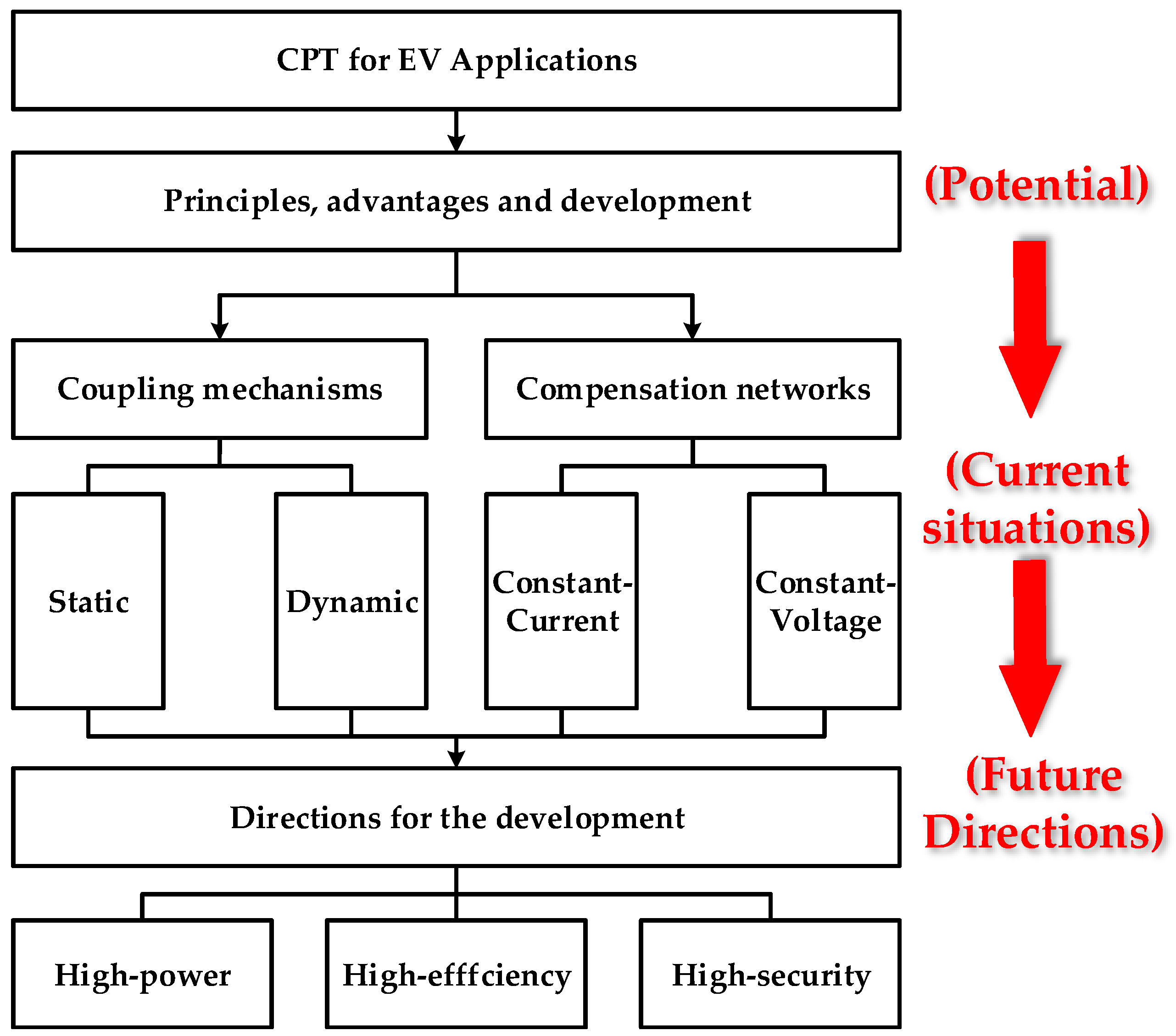
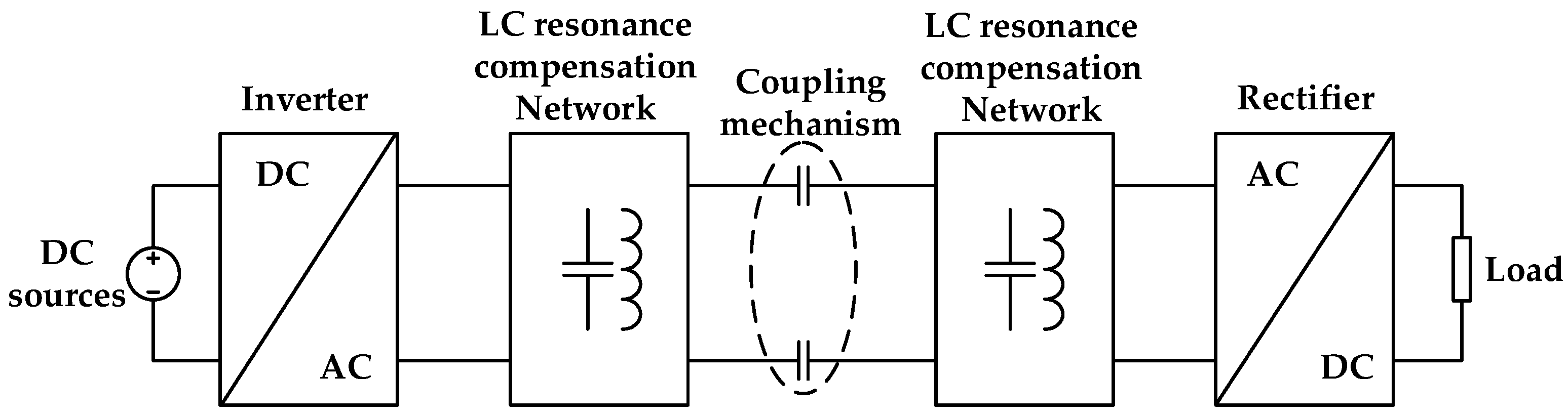
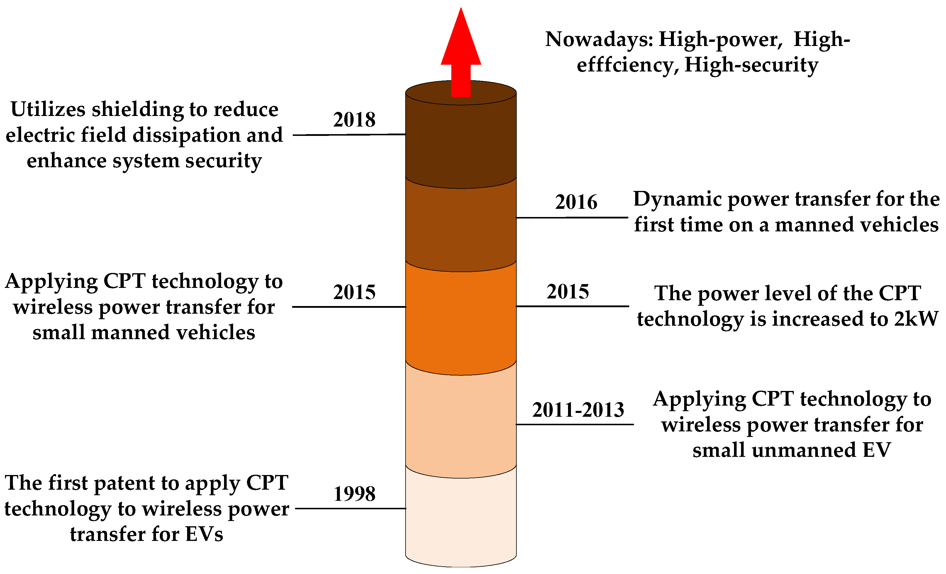
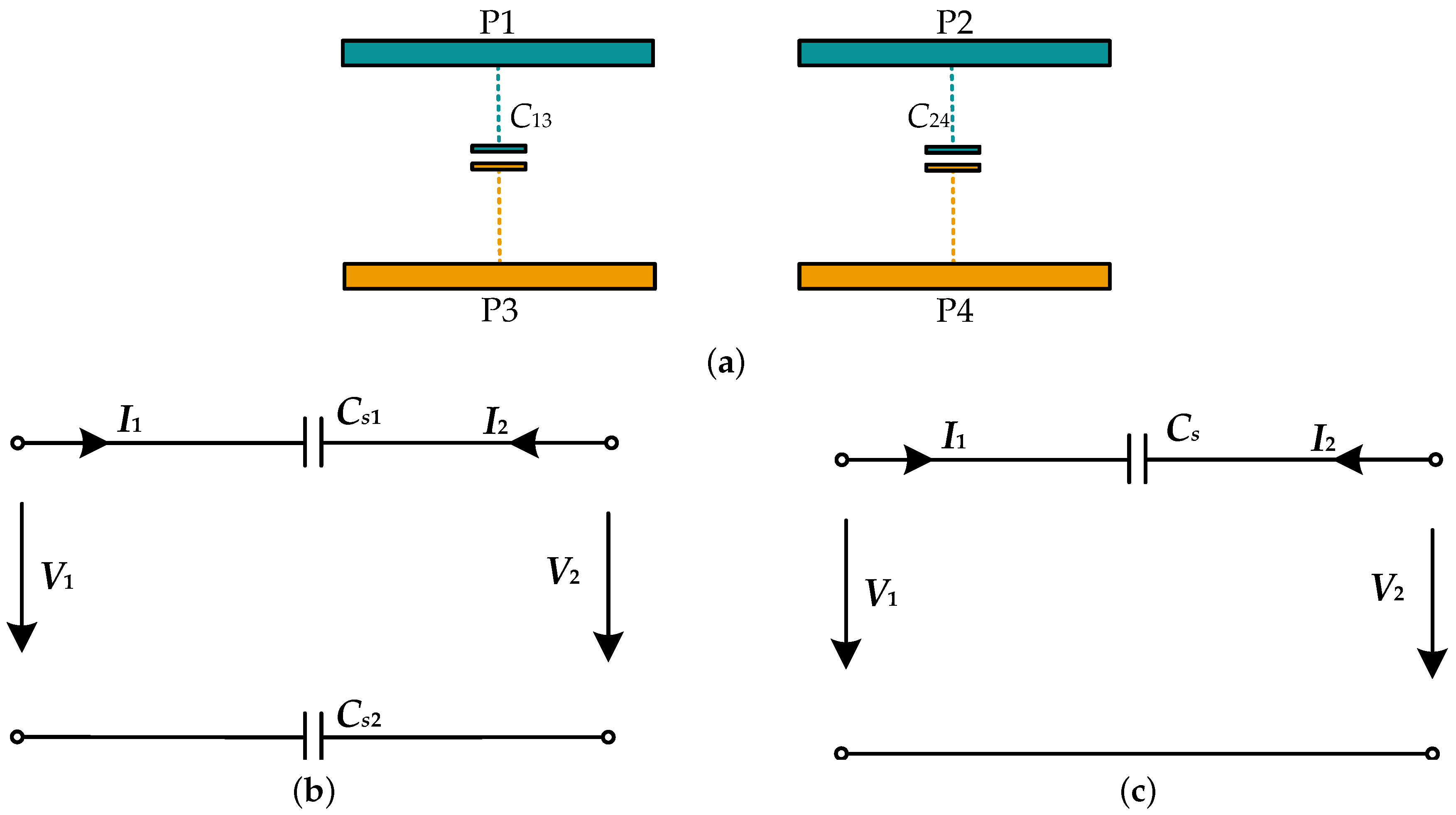
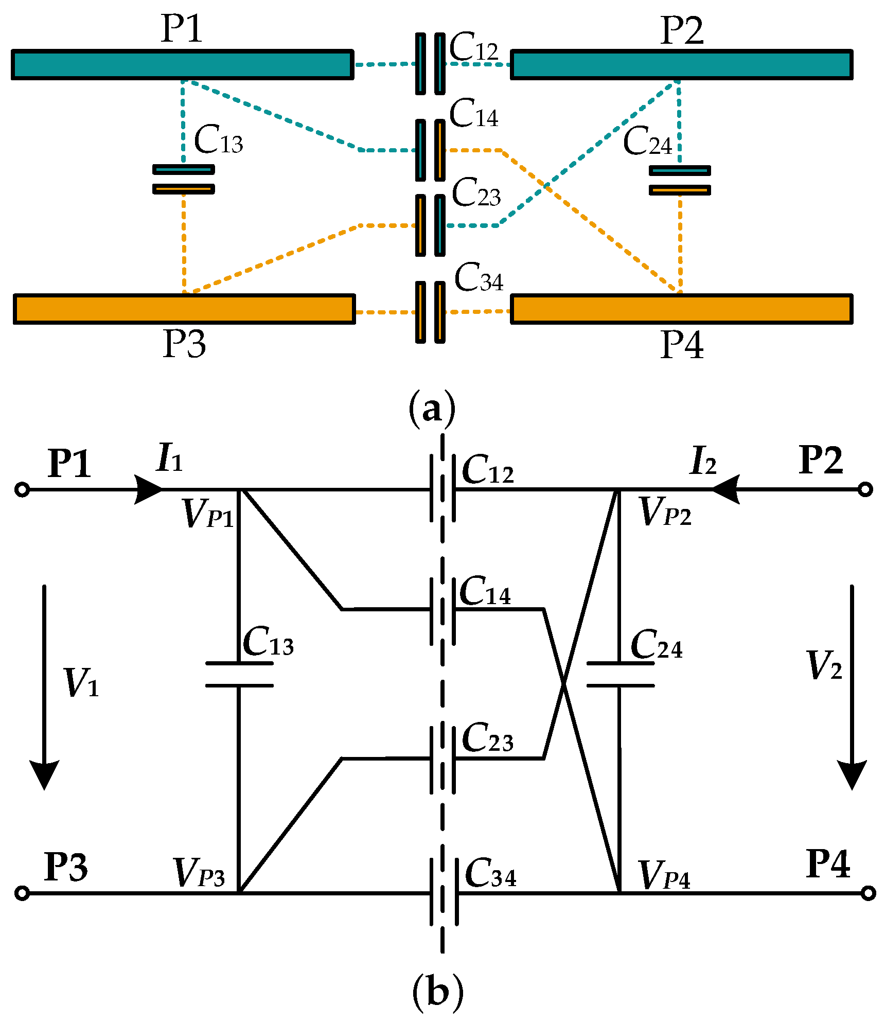
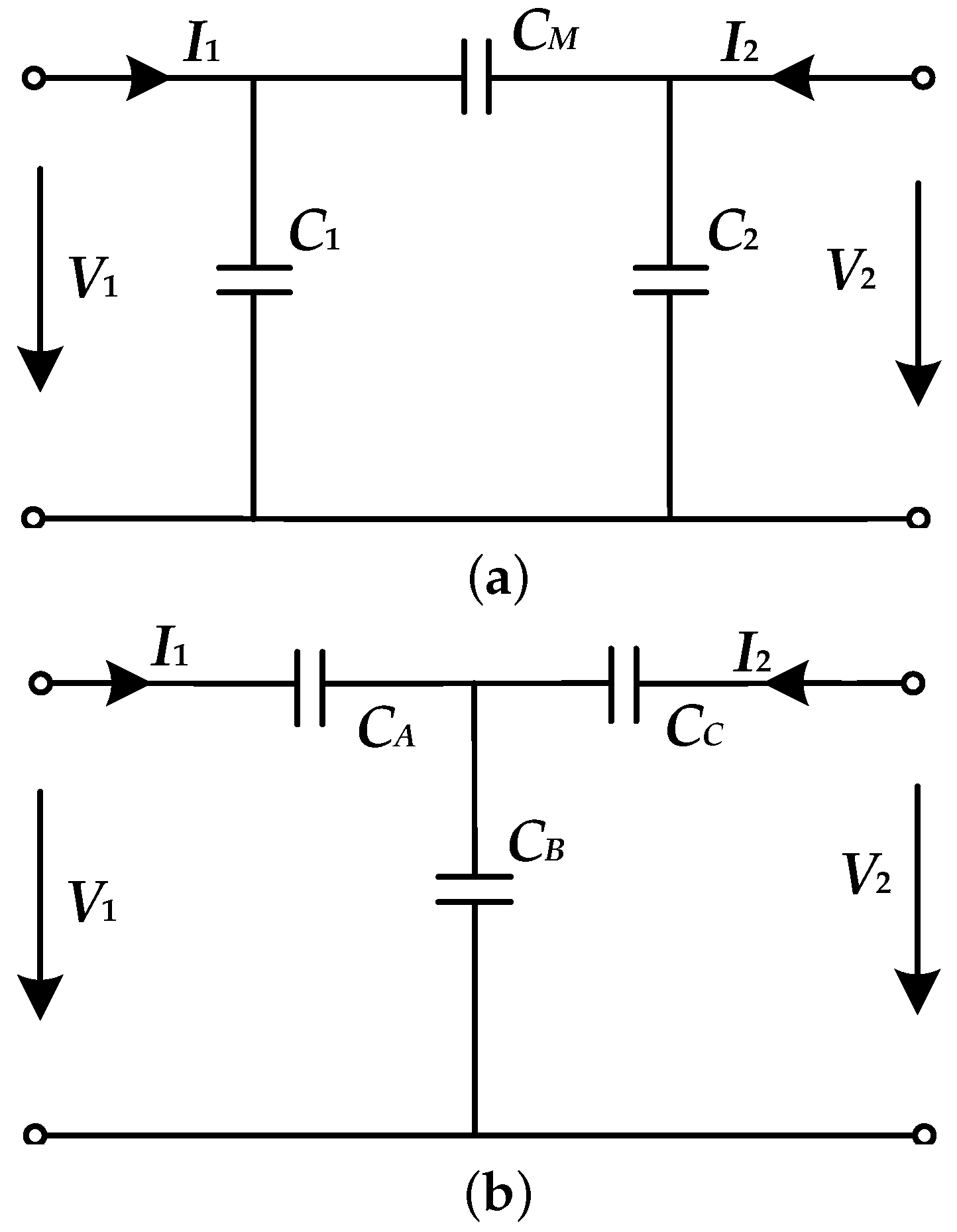

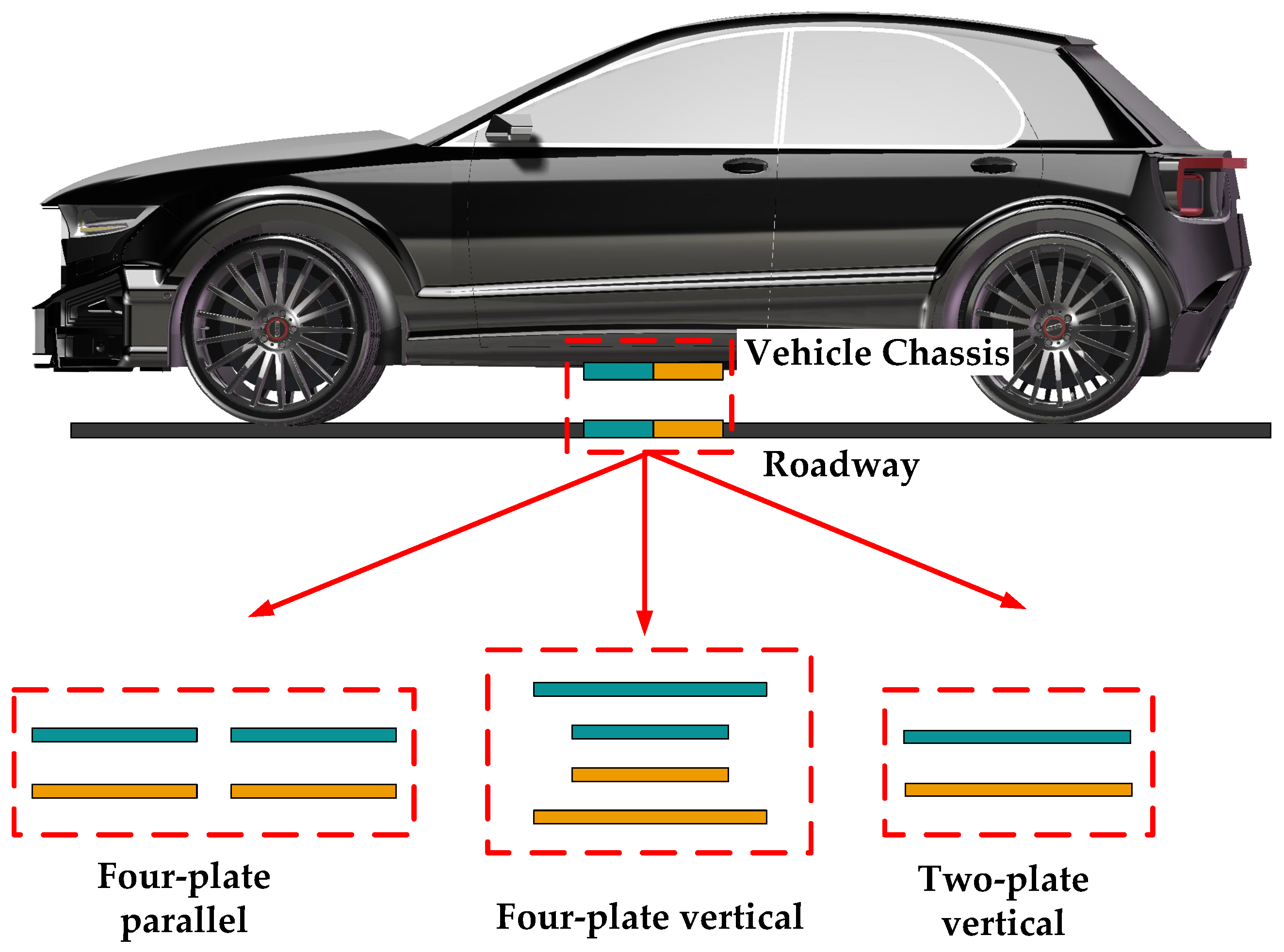
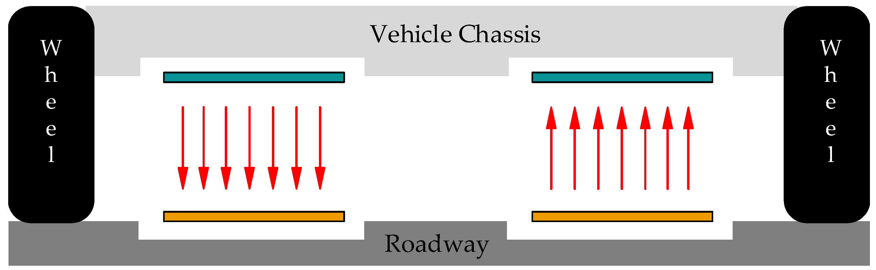


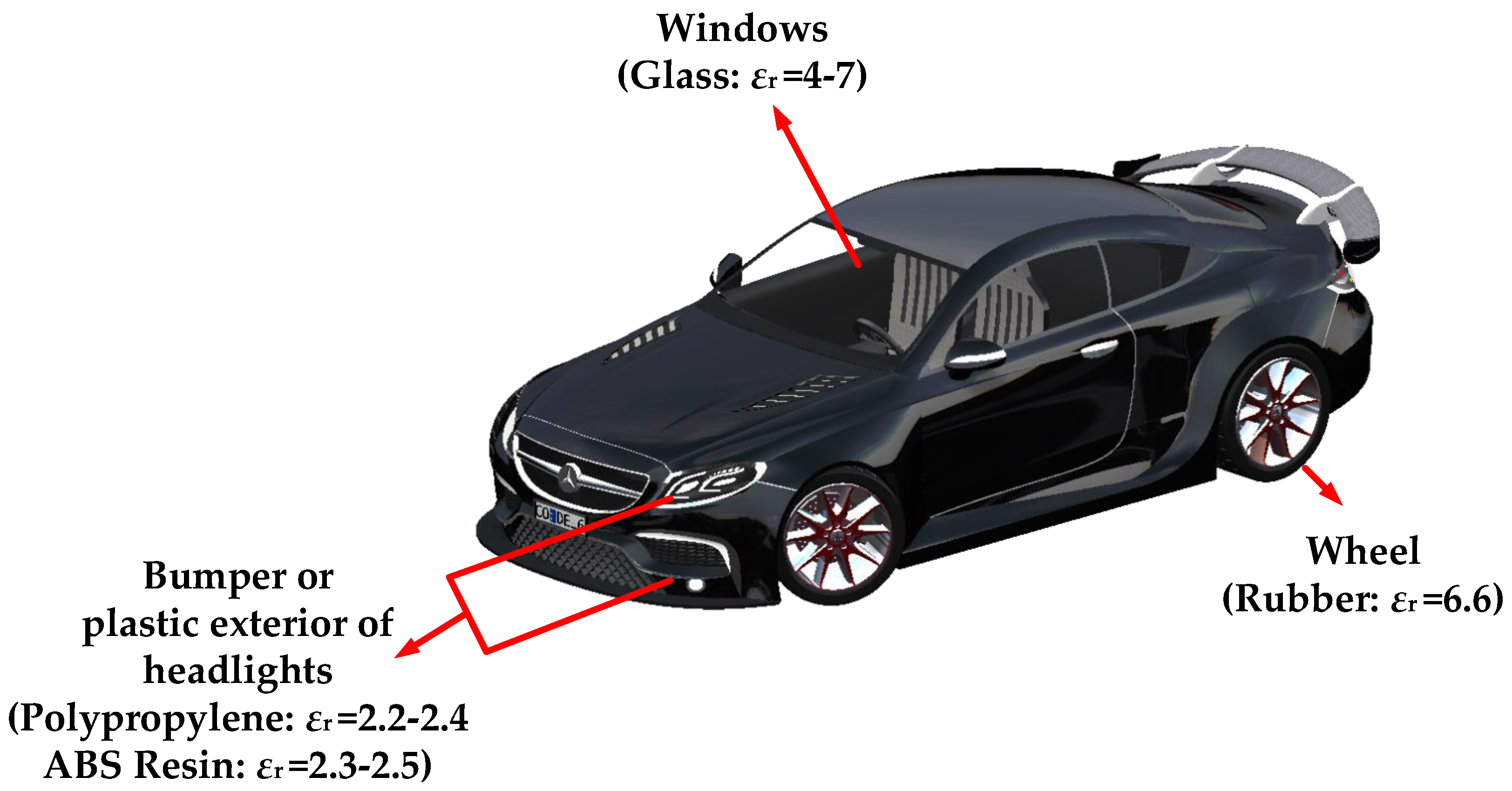
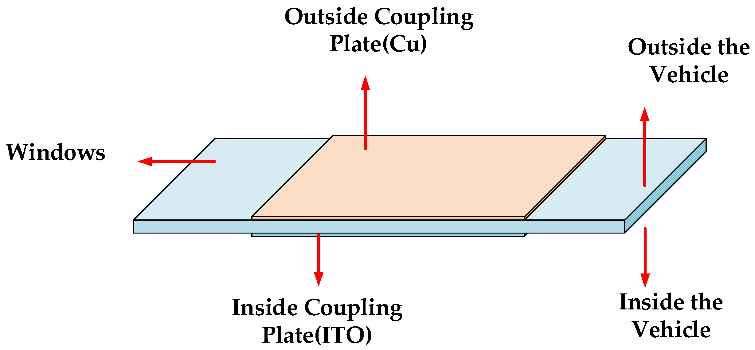
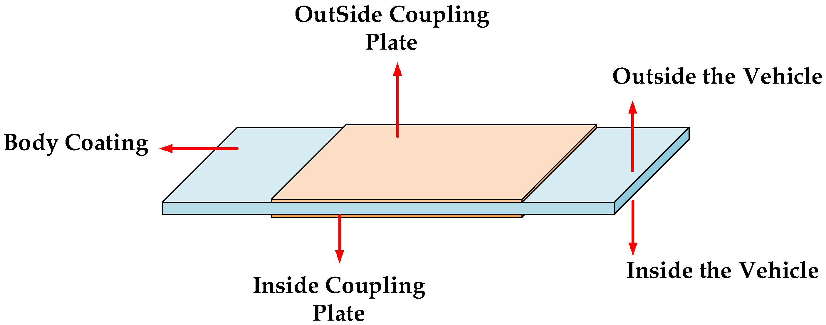


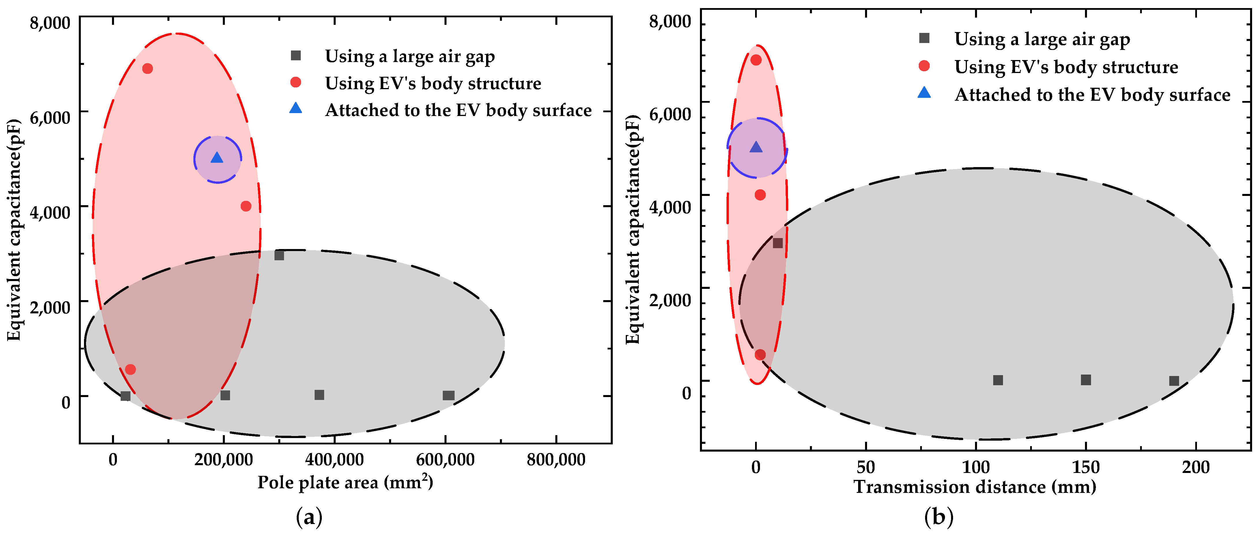
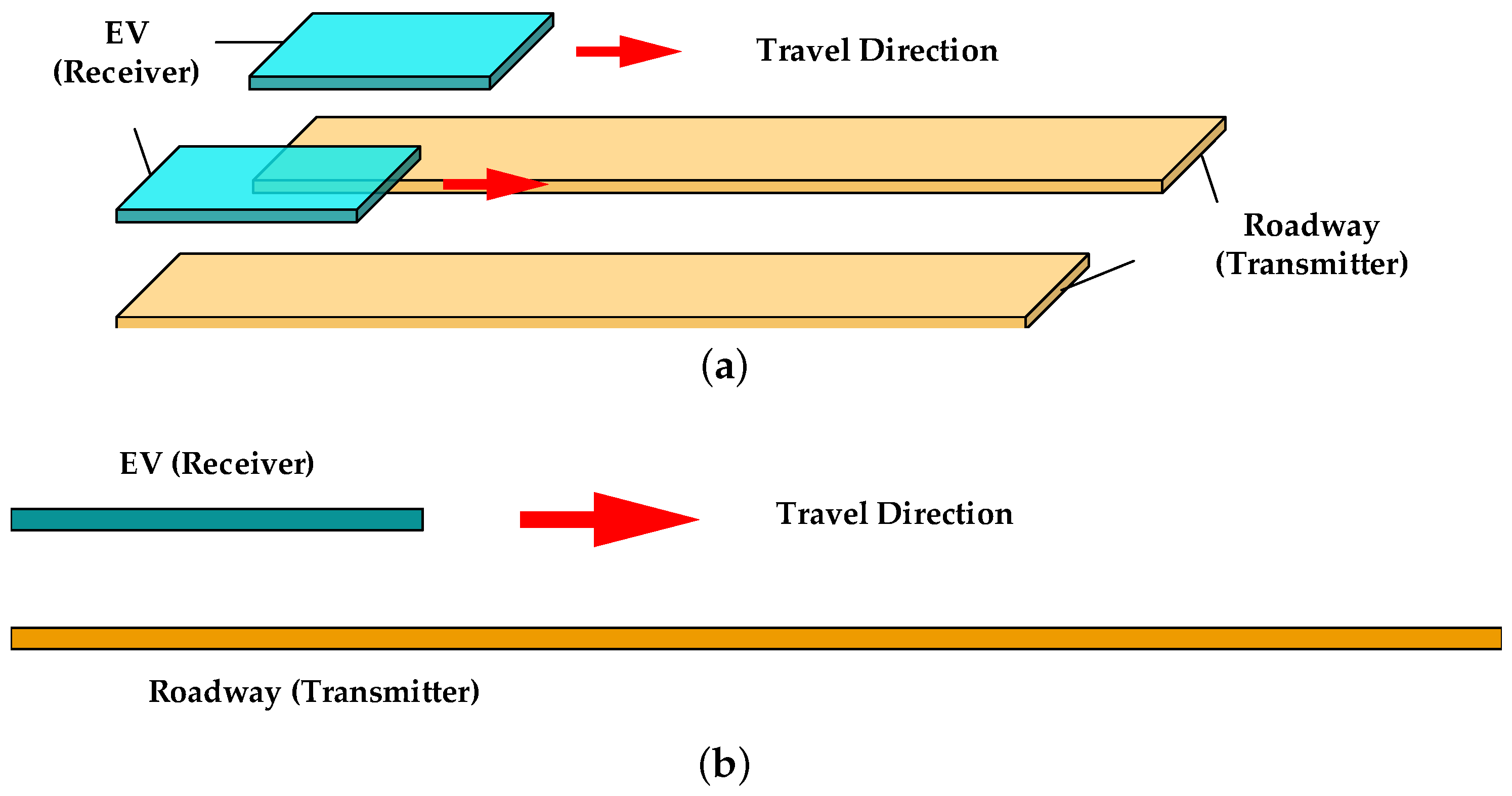
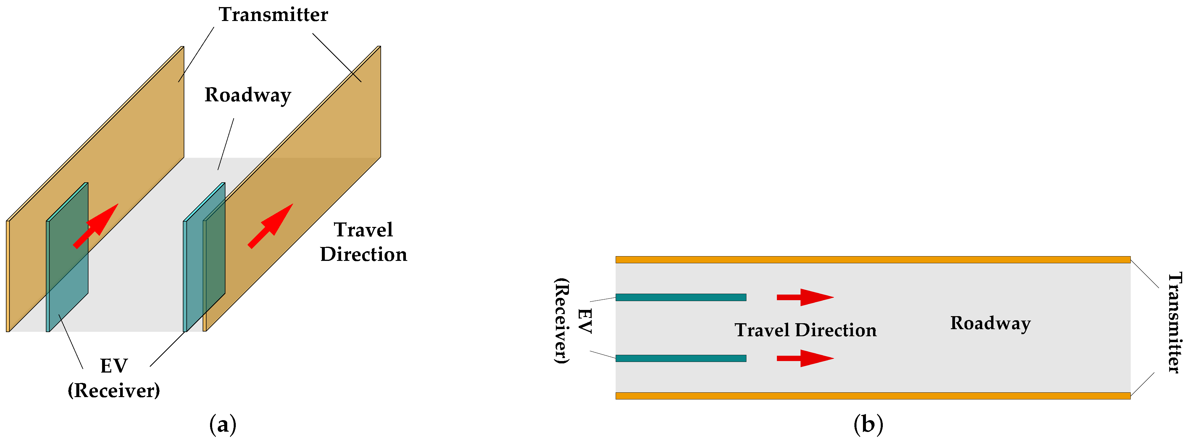


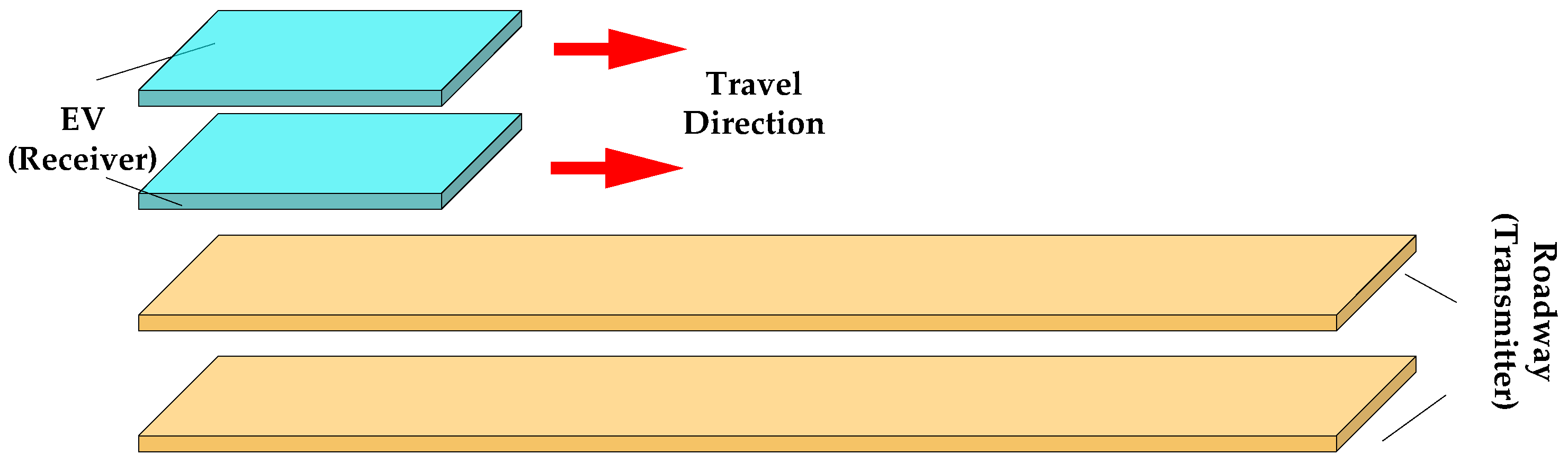
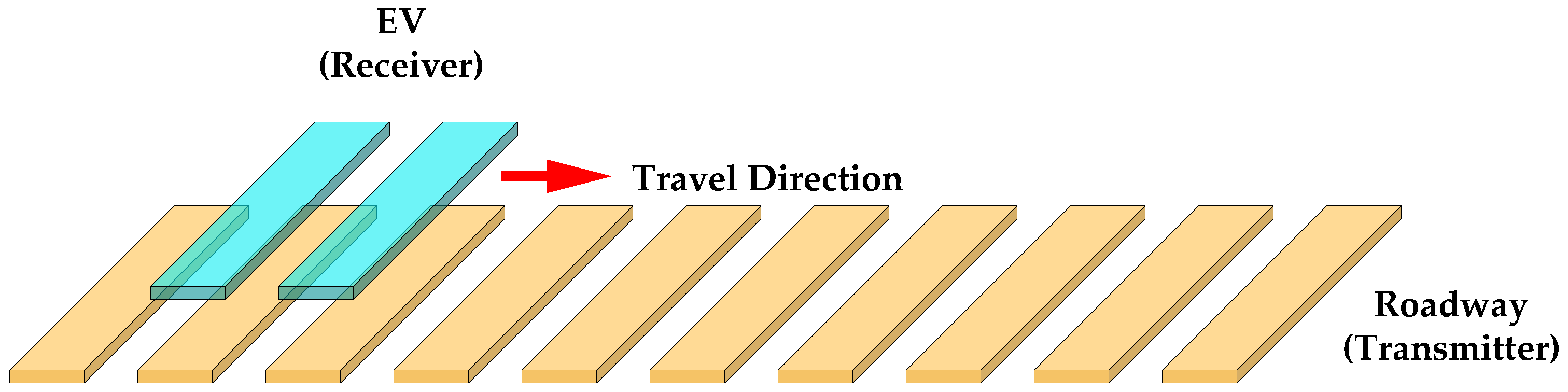
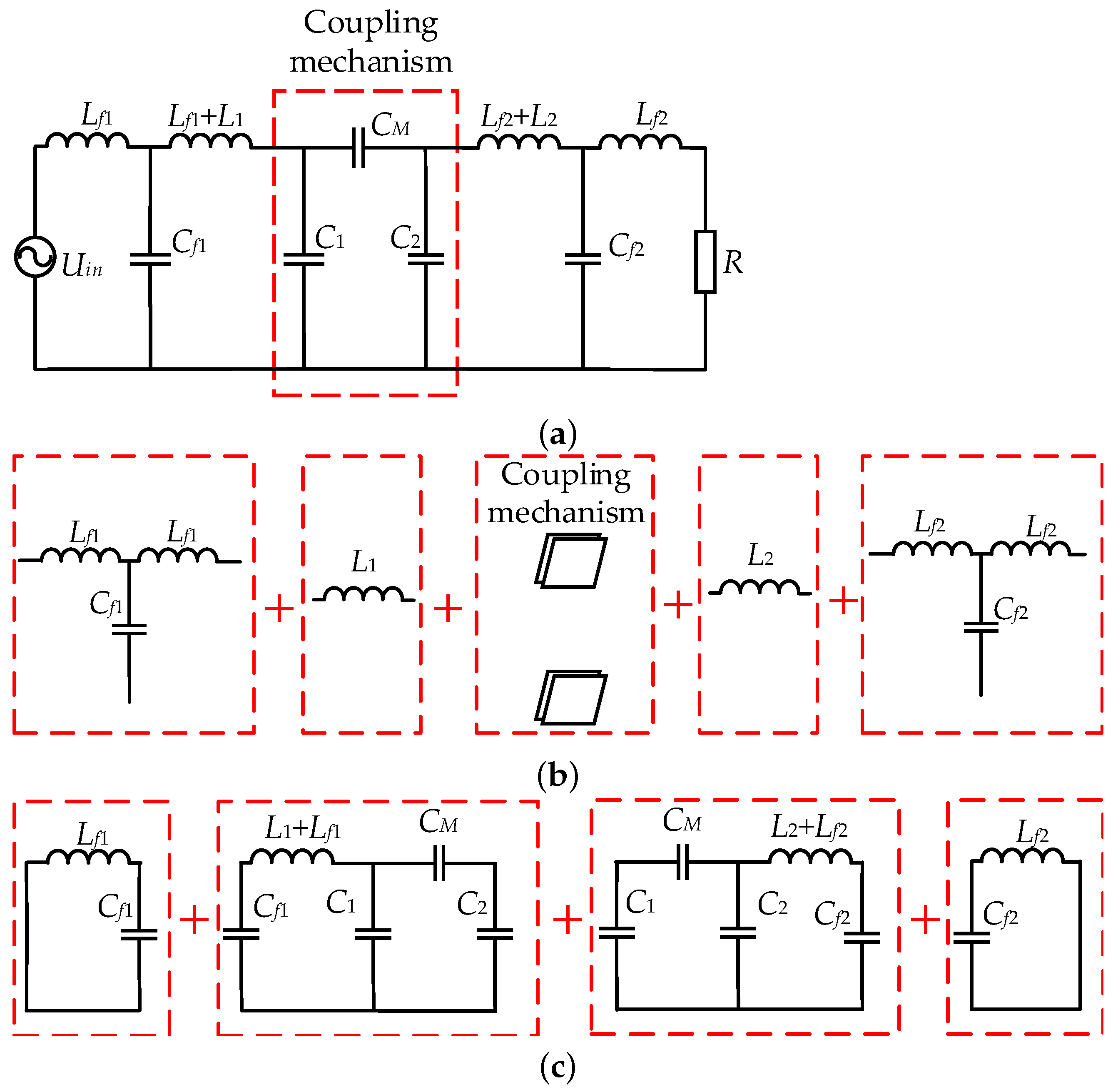
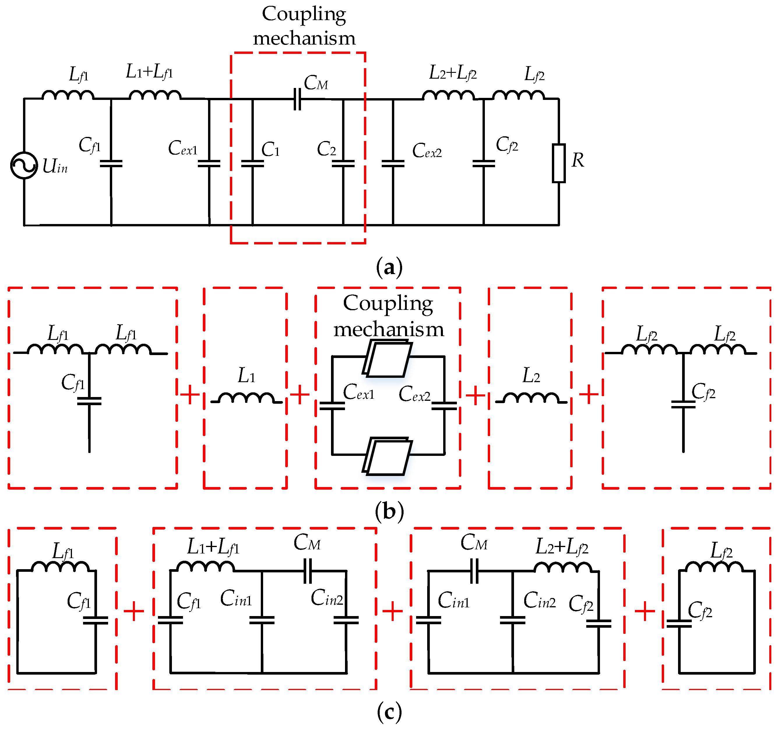
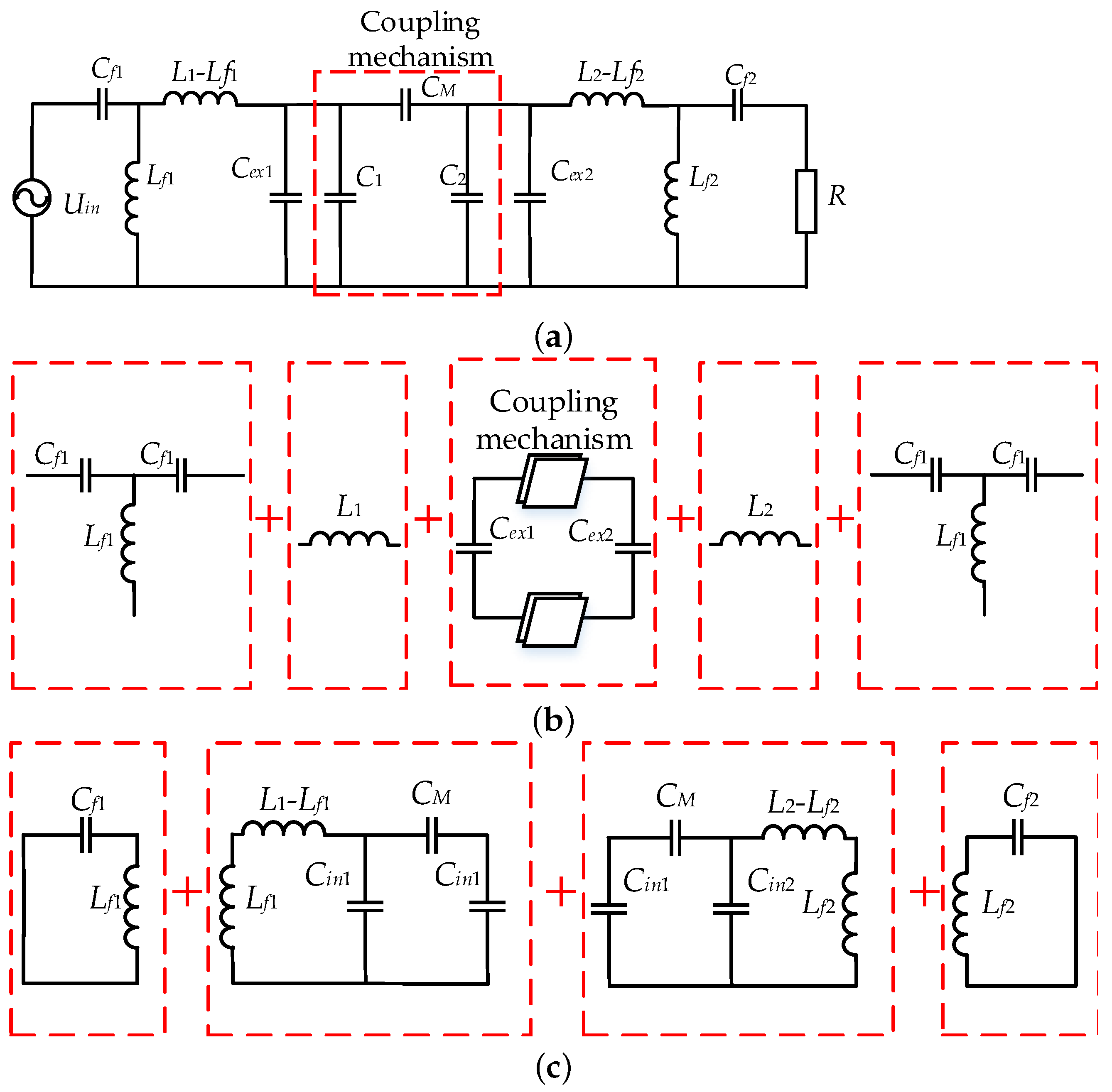
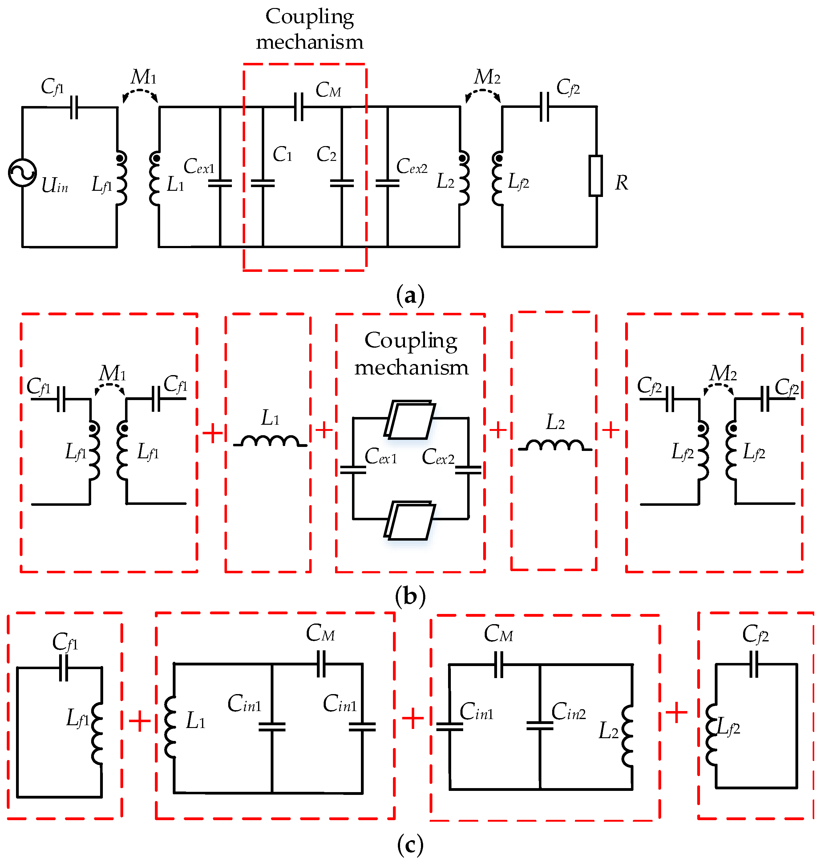
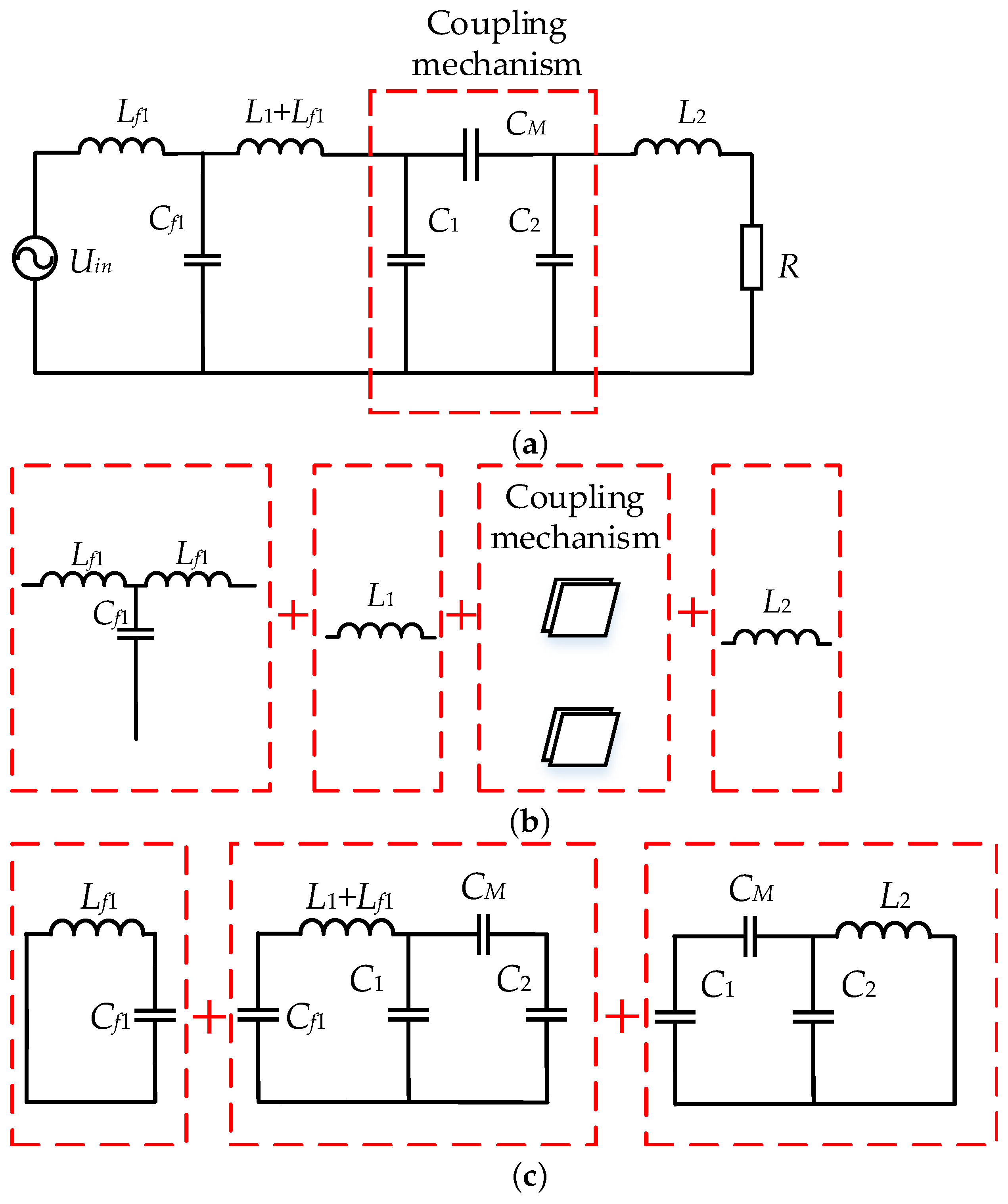

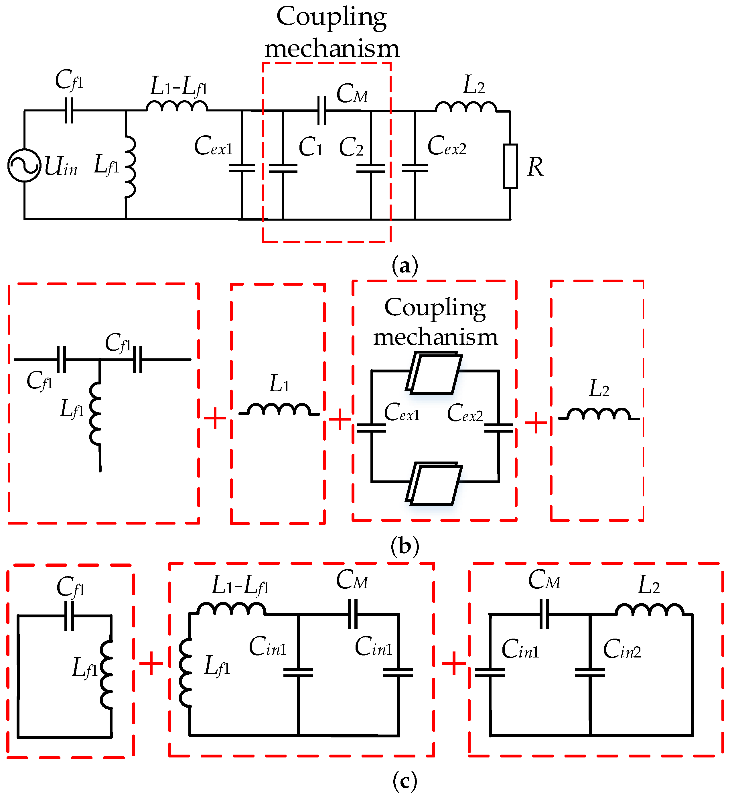

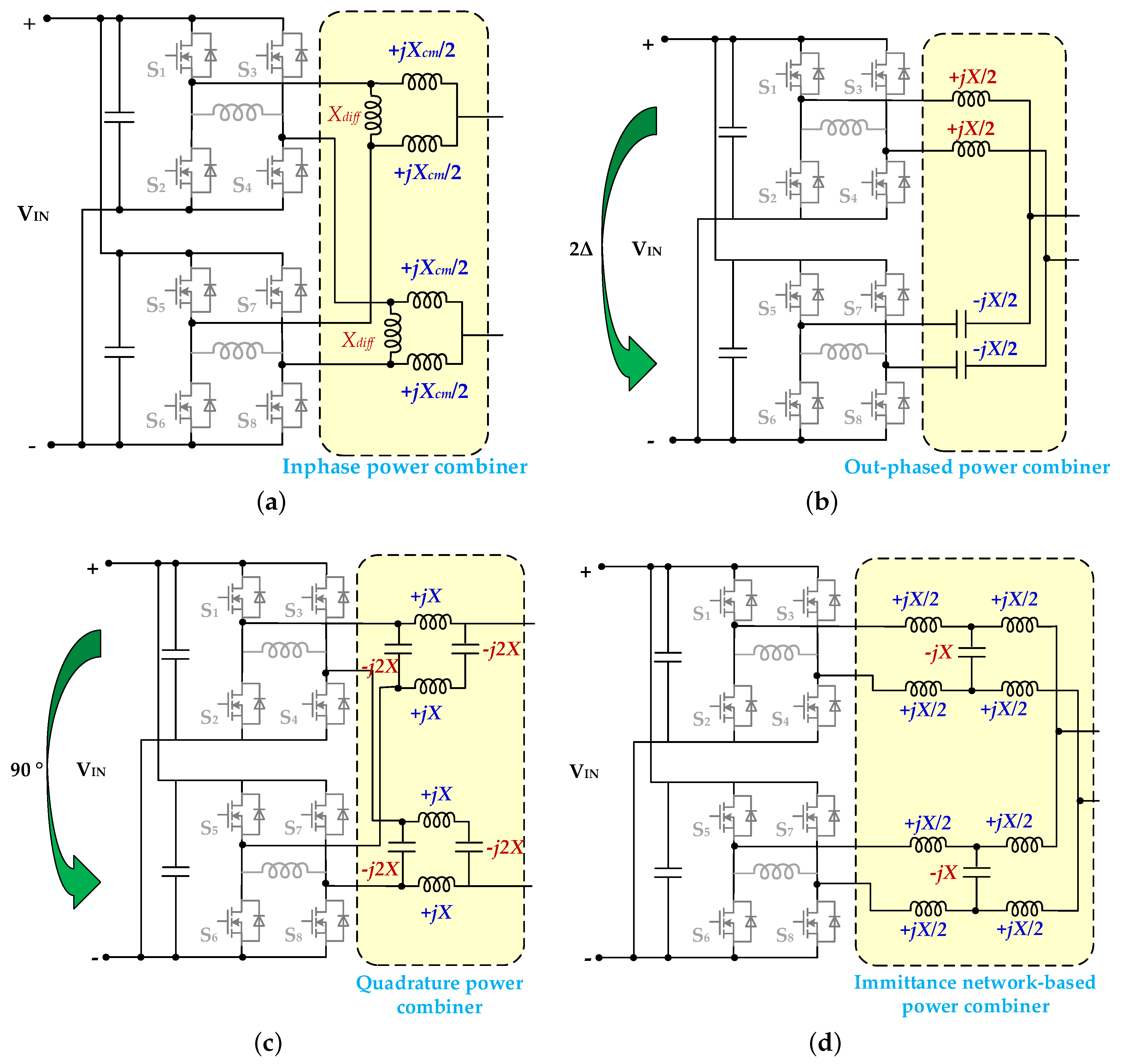

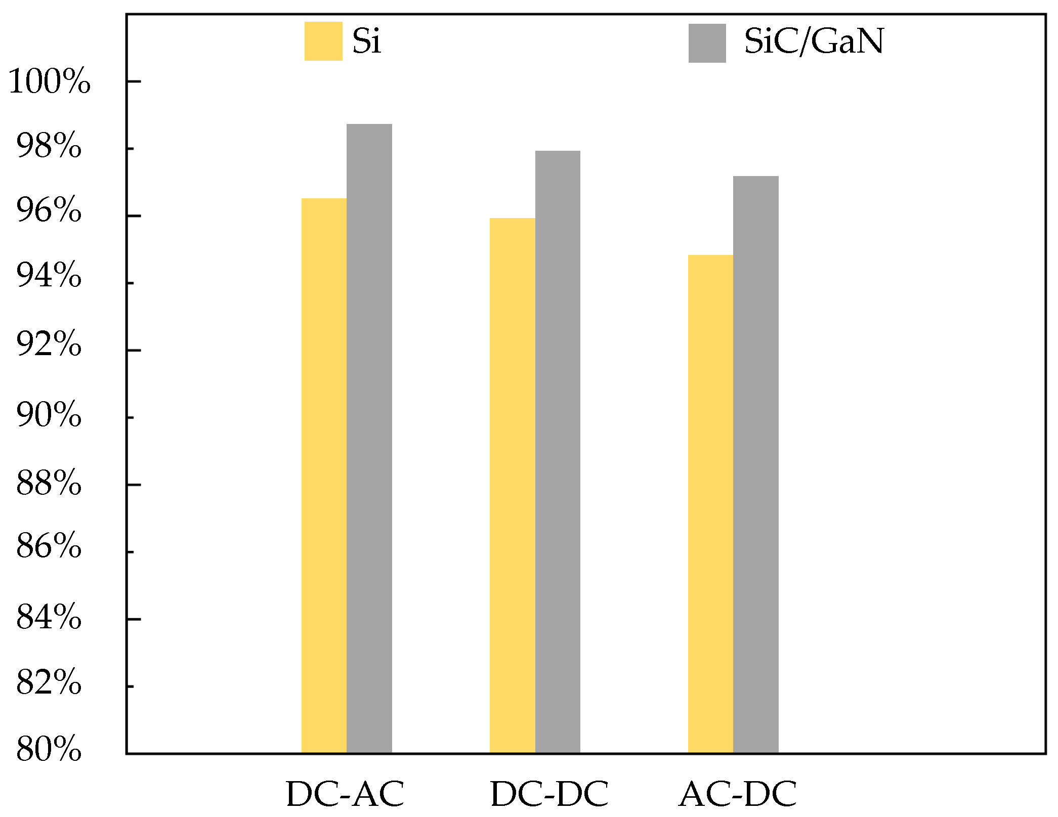

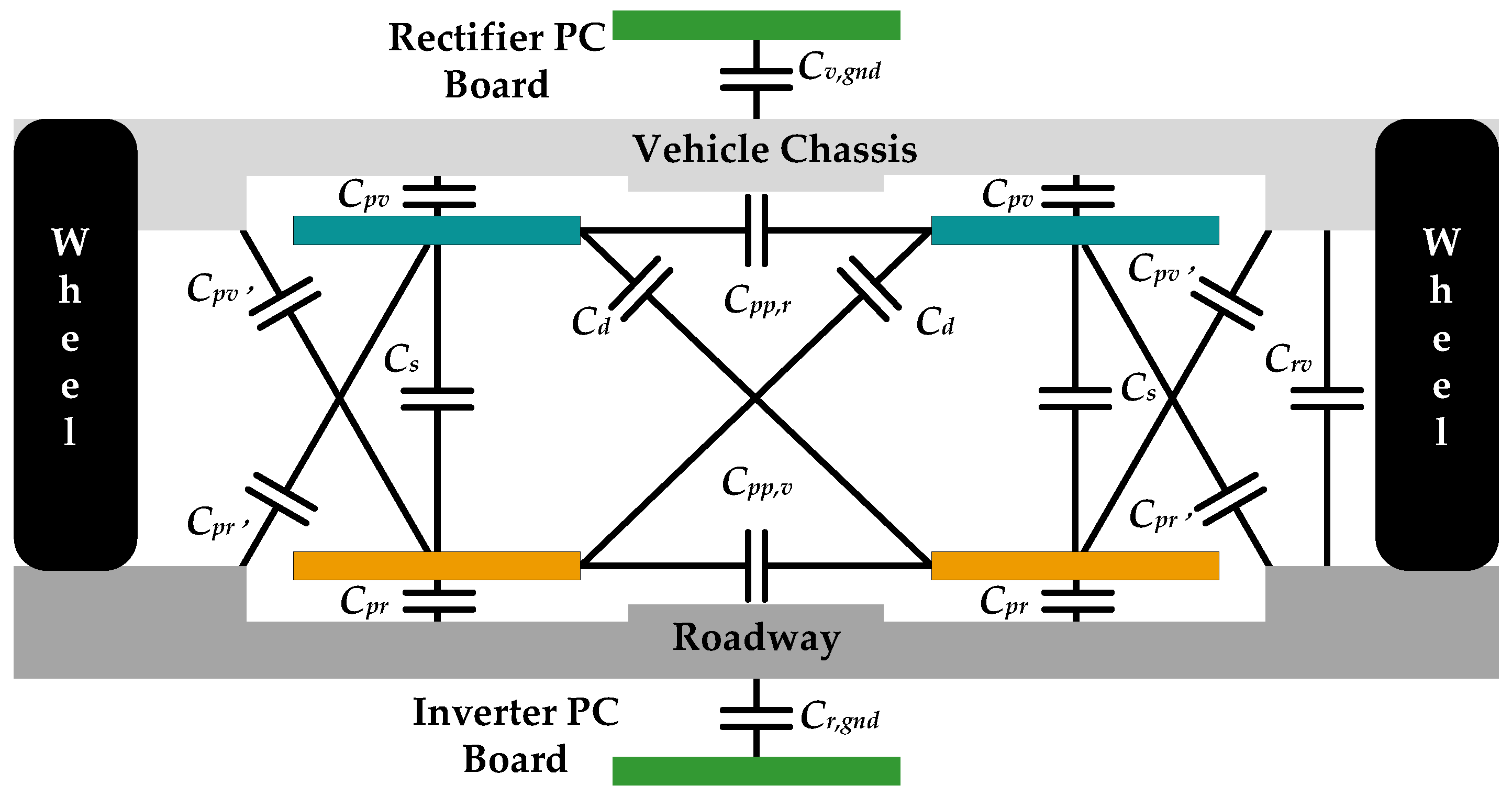
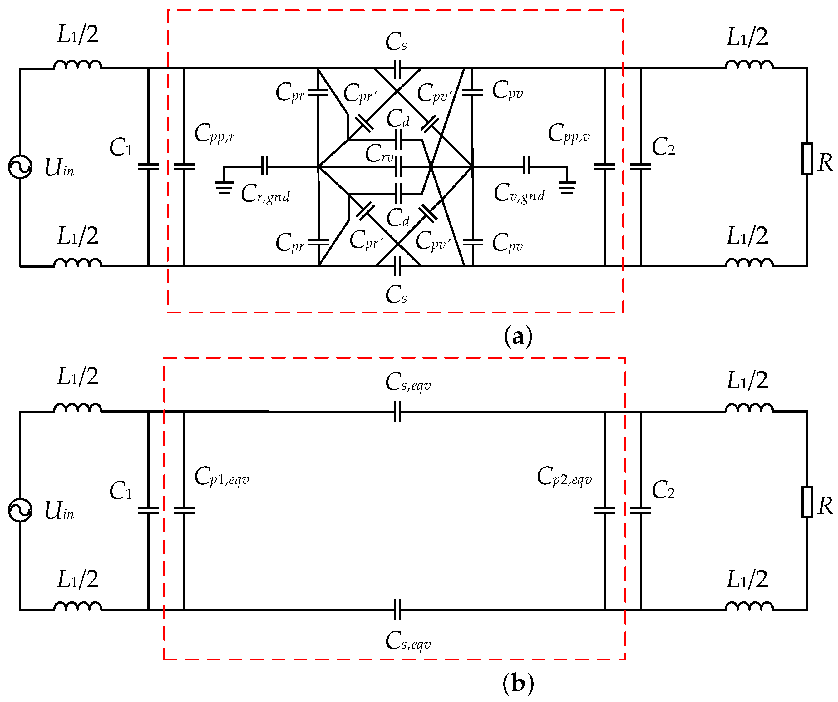
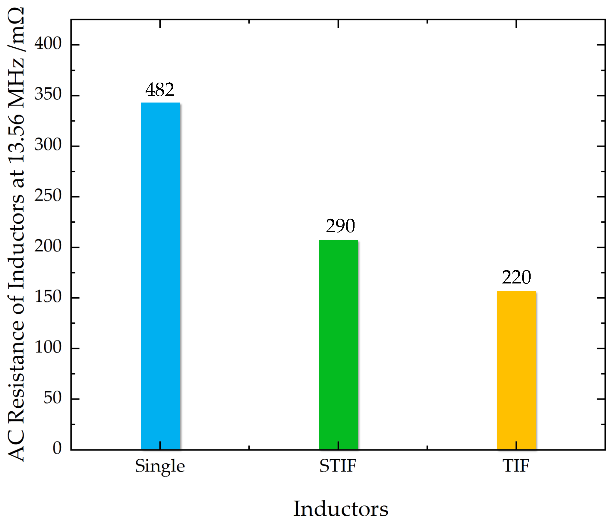
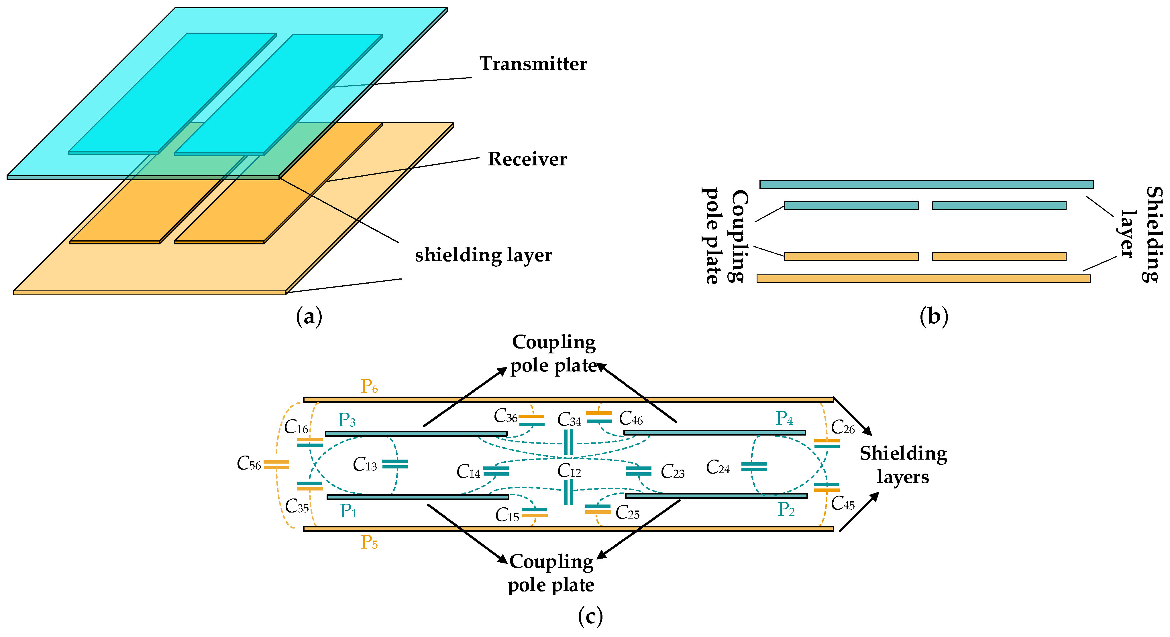

Disclaimer/Publisher’s Note: The statements, opinions and data contained in all publications are solely those of the individual author(s) and contributor(s) and not of MDPI and/or the editor(s). MDPI and/or the editor(s) disclaim responsibility for any injury to people or property resulting from any ideas, methods, instructions or products referred to in the content. |
© 2023 by the authors. Licensee MDPI, Basel, Switzerland. This article is an open access article distributed under the terms and conditions of the Creative Commons Attribution (CC BY) license (https://creativecommons.org/licenses/by/4.0/).