Article

A Wideband Power Amplifier in 65 nm CMOS Covering 25.8 GHz–36.9 GHz by Staggering Tuned MCRs

1
Research and Development Center of Healthcare Electronics, Institute of Microelectronics of the Chinese Academy of Sciences, Beijing 100029, China
2
Beijing Key Laboratory of RFIC Technology for Next Generation Communications, Institute of Microelectronics of the Chinese Academy of Sciences, Beijing 100029, China
3
University of Chinese Academy of Sciences, Beijing 100049, China
*
Authors to whom correspondence should be addressed.
Electronics 2023, 12(17), 3566; https://doi.org/10.3390/electronics12173566
Submission received: 2 May 2023 / Revised: 23 July 2023 / Accepted: 28 July 2023 / Published: 23 August 2023
(This article belongs to the Topic Advanced mm-Wave and Terahertz Antenna Systems)

Abstract

:
Broadband millimeter-wave power amplifiers have attracted much attention and have wide applications for 5G communication, satellite communication, radar, sensing, etc. Yet, it is challenging to design a power amplifier with broadband small-signal gain and power performance simultaneously. In this study, a transformer-based symmetrical magnetically coupled resonator (MCR) matching network for broadband output matching and stagger-tuned MCRs are used to achieve both broadband small- and large-signal performance. Also, to enhance the gain for the power amplifier, a three-stage common-source pseudo-differential structure is adopted to mitigate the low-gain issue due to stagger tuning, and the shunt resistors aimed to decrease the Q factor of the MCRs. We used the in-phase two-way current combined with microstrip transmission lines to increase the output power. Designed in 65 nm bulky CMOS technology, the power amplifier presents a 3 dB small-signal gain bandwidth from 25.8 GHz to 36.9 GHz, indicating a peak gain of 25.87 dB at 30.5 GHz. The power amplifier demonstrates a 17.84 dBm saturated output power ( P s a t ) at 31 GHz and a 24.37% peak power added efficiency ( P A E m a x ) at 28 GHz. The power amplifier achieves a flat P s a t of 17.44 ± 0.4 dBm, a P A E m a x of 22.59 ± 1.78%, and an O P 1 d B of 13.78 ± 0.31 dBm from 26 GHz to 36 GHz.

1. Introduction

The development of 5G communication, satellite communication, and radar has attracted much interest and acquired great demands in high-rate wireless communication. There are mainly two ways to increase the data transmission rate: (1) improve the spectrum efficiency; (2) increase the bandwidth of the spectrum. With the same spectrum efficiency, the data transmission rate increases twice with the doubled bandwidth [1]. In the wideband millimeter-wave band region, an extreme data rate is delivered even under low-order modulation [2]. Also, the higher frequency decreases the antenna size, which is important for phase-array design [1]. The frequency regions n257 (26.5–29.5 GHz), n258 (24.25–27.5 GHz), and n260 (37–40 GHz) are specified as 5G FR2 frequency ranges by the 3 GPP 5G New Radio (NR) Standard [3,4]. Countries have adopted different frequency bands for 5G or other applications. If a single transmitter possesses the bandwidth to cover multiple or all of the regional frequency bands, it can roam internationally [1,5,6], which reduces the system cost and design difficulty. Also, for an FMCW radar, wideband is necessary for improving the range resolution ( R ) [7,8], which is estimated using
R = c ( 2 B W )
in which BW is the bandwidth of the radiated chirp [8]. Power amplifiers (PA), one of the most important blocks in millimeter-wave transmitters, have attracted more and more attention, with their output power and bandwidth having important effects on the whole system. The output power of the PA determines the signal distance, and the bandwidth greatly influences the data transmission rate. The challenge of designing a broadband PA is to sustain the wideband small-signal frequency response and broadband power performance simultaneously [9]. There are mainly four ways to achieve wideband millimeter-wave silicon-based power amplifiers: (1) distributed amplifiers; (2) stagger tuning; (3) high-order matching networks; and (4) feedback networks. Distributed amplifiers usually occupy a large area of chip size [10], and achieving a wideband optimal load impedance is difficult in this way [11]. Also, at each stage of the distributed amplifiers, the load impedance is not the optimal value for power matching, leading to a decreased efficiency of the power amplifiers [12,13]. The stagger-tuning technique makes the multiple amplification stages cascade and resonate at different frequencies to flatten the total gain response [1], which is usually effective to achieve small-signal broadband [14,15]. In addition, the stagger tuning method sacrifices the gain of the amplifier [16]. High-order matching networks, like Chebyshev filters or high-order LC filters, often consist of several passive components, resulting in a high insertion loss. The feedback technique, i.e., resistance–capacitance feedback network, suffers from deteriorated output power and efficiency [7,17]. Transformers or transformer-based magnetically coupled resonators (MCR) are high-order LC networks with only one inductor area that are widely used for wideband power amplifiers and low-noise amplifiers [7,16,18]. Jia et al. designed a wideband power amplifier with a symmetrical transformer-based MCR providing wideband optimal load impedance [16]. Wang et al. demonstrated a compact wideband high-linear-power amplifier covering 24–42 GHz using a custom-designed distributed balun with wideband optimum load impedance [5]. Chou et al. presented a V-Band wideband power amplifier with the help of a transformer-based radial power combiner and the stagger tuning technique [19]. All these power amplifiers use transformer-based or distributed-balun-based MCRs to realize wideband optimal load impedance by carefully selecting the MCR parameters. Wang et al. indicated that a wideband (46–101 GHz) power amplifier with a high-k interstage transformer can be compensated via a single-peak output-matching network [7]. To further decrease the gain ripple, a Gm compensator-based negative feedback chain is also applied. Wei et al. presented a wideband LNA by adding the peaks and valleys of the different resonators [18]. Xue et al. [20] proposed two W-Band wideband power amplifiers by staggering the transformers’ resonating frequency using an in situ transformer-coupled resonating peak control simulation methodology to realize 9/16 GHz 3 dB small-signal bandwidth. In reference [21], the transformer-based resonating peak tuning and staggering method was also used to achieve two wideband power amplifiers covering the 16/14 GHz 3 dB small-signal bandwidth. Several studies [18,20,21] have adopted the transformer-based staggering method and only small-signal wideband performance was achieved. Meanwhile, the design of the transformer-based staggering method lacks detailed elaboration. For example, reference [20] used a staggering method to flatten the bandwidth but without detailed method processes and particulars. In our work, we give not only the detailed design process but also the detailed whole logical thinking perspectives and design method for a wideband power amplifier. In this work, a symmetrical transformer-based output MCR4 is used to provide wideband optimal load impedance for the power stage. At the interstage between the power stage and driver stage 2, an asymmetrical MCR3 is used to realize wideband matching by making it satisfy both the conditions of ω 1 = ω 2 and a good matching at 35 GHz. At the interstage between driver stage 1 and driver stage 2, an asymmetrical MCR2 to form a high-pass form Z21 for stagger tuning is realized by selecting the transformer parameters under the condition of matching at 33 GHz. The input asymmetrical MCR1 is used to achieve wideband response and to compensate for the gain decline at the band edge ( f L and f H ). The symmetrical output MCR4 for wideband optimal Z o p t (leading to wideband large-signal performance) and stagger-tuned interstage and input MCRs for flattened small-signal bandwidth are combined for a better performance. The framework of the paper is organized as follows: A detailed analysis of the design of the four MCRs for input, output, and interstage matching is introduced in Section 2. Section 3 presents the whole circuit design consideration of the power amplifier. Section 4 shows the simulation results, and Section 5 concludes the entire work.

2. Analysis and Design

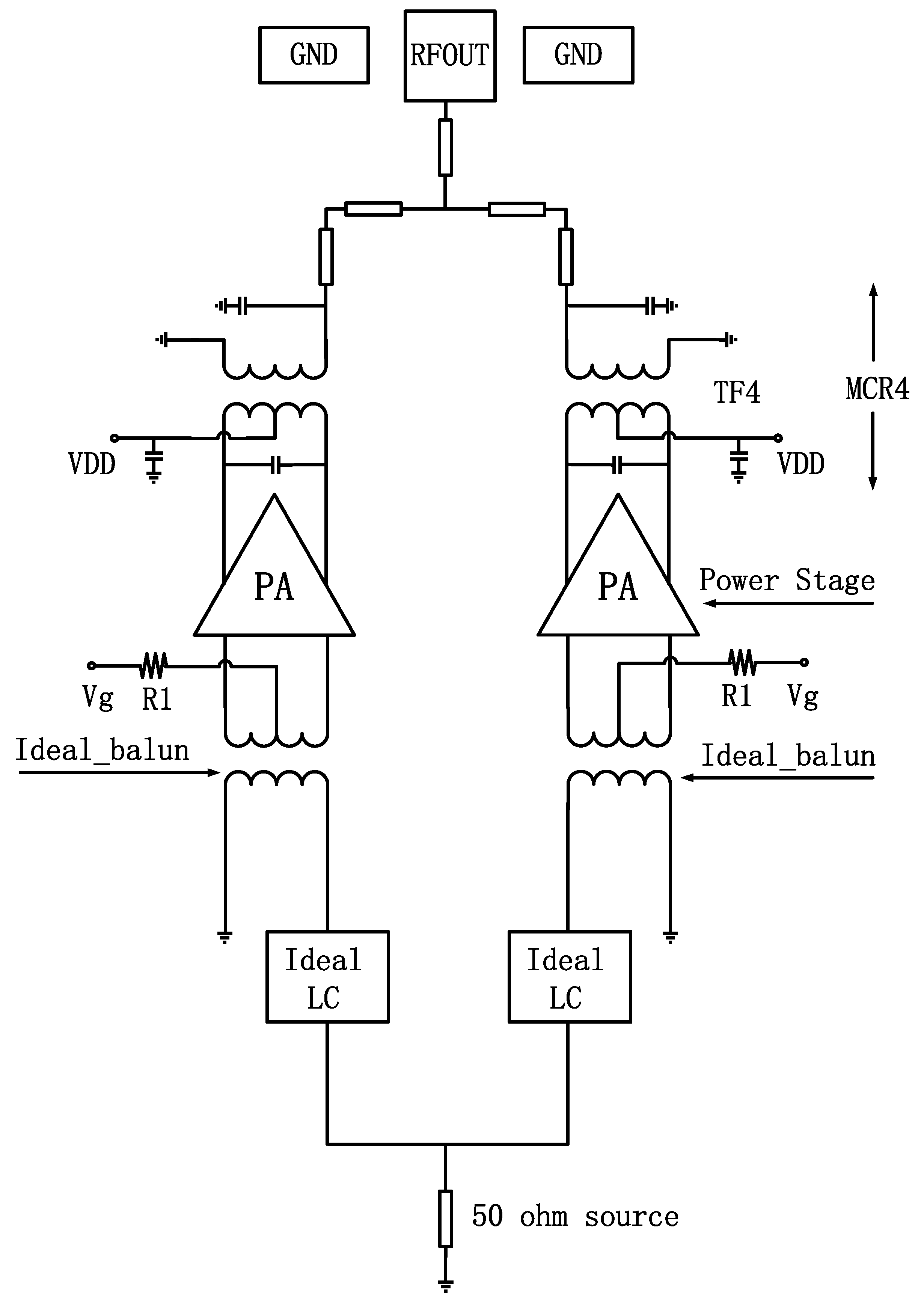
Figure 1a is the schematic of the designed broadband power amplifier. To increase the output power, two-way current-combining is used with stronger symmetry than voltage-combining [22]. Figure 1b is the cell stage of the power amplifier. In this work, we aim to design the output matching network for realizing a wideband Z o p t for the power stage. The interstage matching network between power stage and driver stage 2 is used to achieve wideband impedance matching. We also design the interstage matching between driver stage 2 and driver stage 1 to realize a high-pass form filter for the staggering. The input-matching network is used to tune the gain shape of its stage by adopting a ω / Q -compensated asymmetrical MCR to enhance the gain at the band edge ( f L and f H ), so that a flattened wideband performance of the whole circuit is achieved.

2.1. Wideband Output Matching Network Design

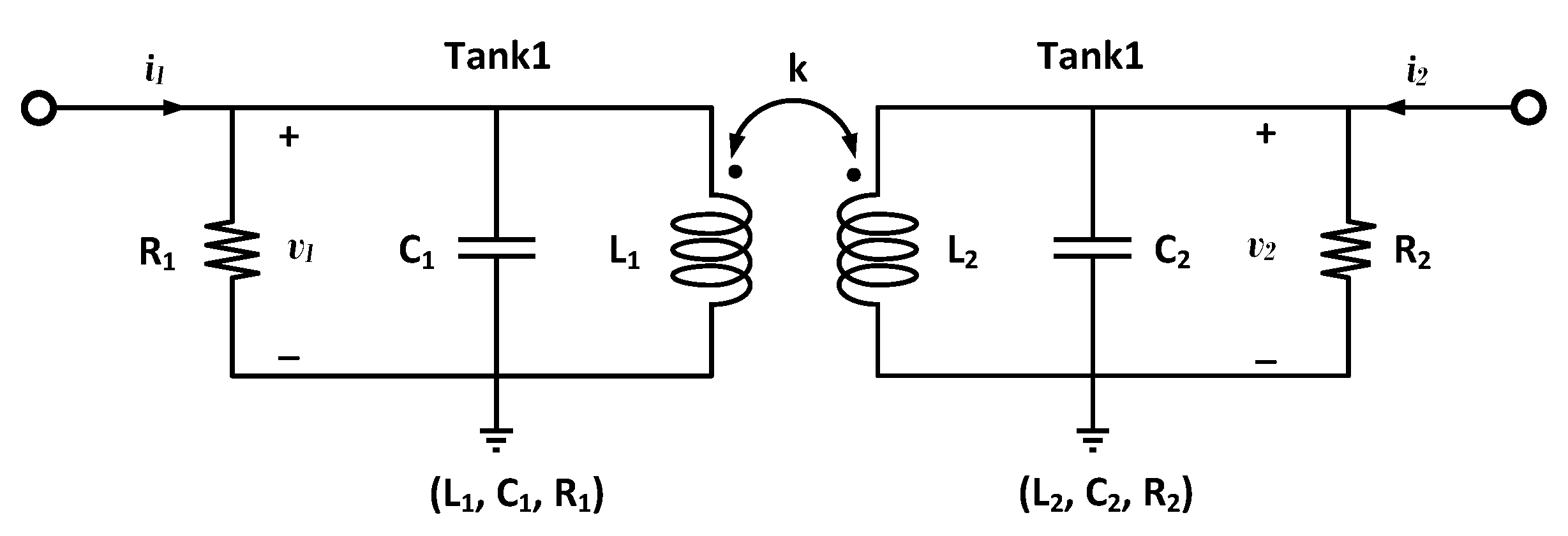
Wideband output matching network, which transfers the load impedance to Z o p t for the power stage in a wideband frequency range, is the key factor for large power characteristics of a PA [23]. A symmetrical MCR could be used to achieve the broadband Z o p t [16]. In a symmetrical MCR, as shown in Figure 2,
Q 1 = Q 2 = Q 0
ω 1 = ω 2 = ω 0
in which
Q 0 = Q 1 = Q 2 = ω 1 R 1 C 1 = ω 2 R 2 C 2
ω 0 = ω 1 , 2 = 1 L 1 C 1 = 1 L 2 C 2
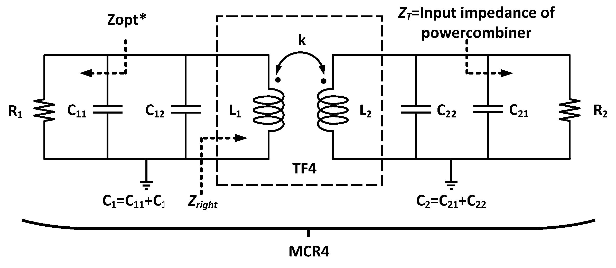
K is the coupling coefficient between the two inductors, as shown in Figure 2. In this work, the interest frequency band is from 26 GHz to 36 GHz. As the output power and power gain at low frequency is larger than that at high frequency, we choose 32 GHz rather than 31 GHz as the center operation frequency to calculate the parameters of the output-matching MCR. Based on the loadpull simulation, we choose Z o p t = (26 + j*26) Ω for the power stage at 32 GHz. The conjugate of Zopt is Z o p t = (26 − j*26) Ω , which is equivalent to a resistor of R 1 = 52 Ω parallel with a capacitor of C 11 = 95.65 fF, as shown in the lumped model of the output symmetrical MCR in Figure 3. The symmetrical MCR transfers the input impedance of the power combiner to Z o p t for the power stage. The power combiner at the output, as shown in the dashed line on the top of Figure 1a, is designed to reactively transfer the load impedance to Z T = (27.86 − j*25.96) Ω for the output transformer by using microstrip transmission-line segments. In the output symmetrical MCR shown in Figure 3, C 1 = C 11 + C 12 , C 2 = C 21 + C 22 . C 12 represents the extra added capacitor on the primary side if needed. C 21 represents the equivalent paralleled output capacitance of the power combiner input impedance ( Z T ), which is 89 fF in this work. C 22 represents the extra added capacitor on the right side if needed. R 2 represents the equivalent paralleled output resistor of the power combiner input impedance ( Z T ), which is also 52 Ω in this work. For a symmetrical MCR, the coupling factor k and Q factor satisfy the equations below under the no in-band ripple condition [16]:
Q = 1 + 1 + 4 ( ω c R 1 C 1 ) 4 2
k = 1 1 + Q 2
L 1 = R 1 2 C 1 Q 2
L 1 L 2 = R 1 R 2
C 2 = R 1 R 2 C 1
in which ω c is the center operation frequency with 32 GHz, as mentioned above.
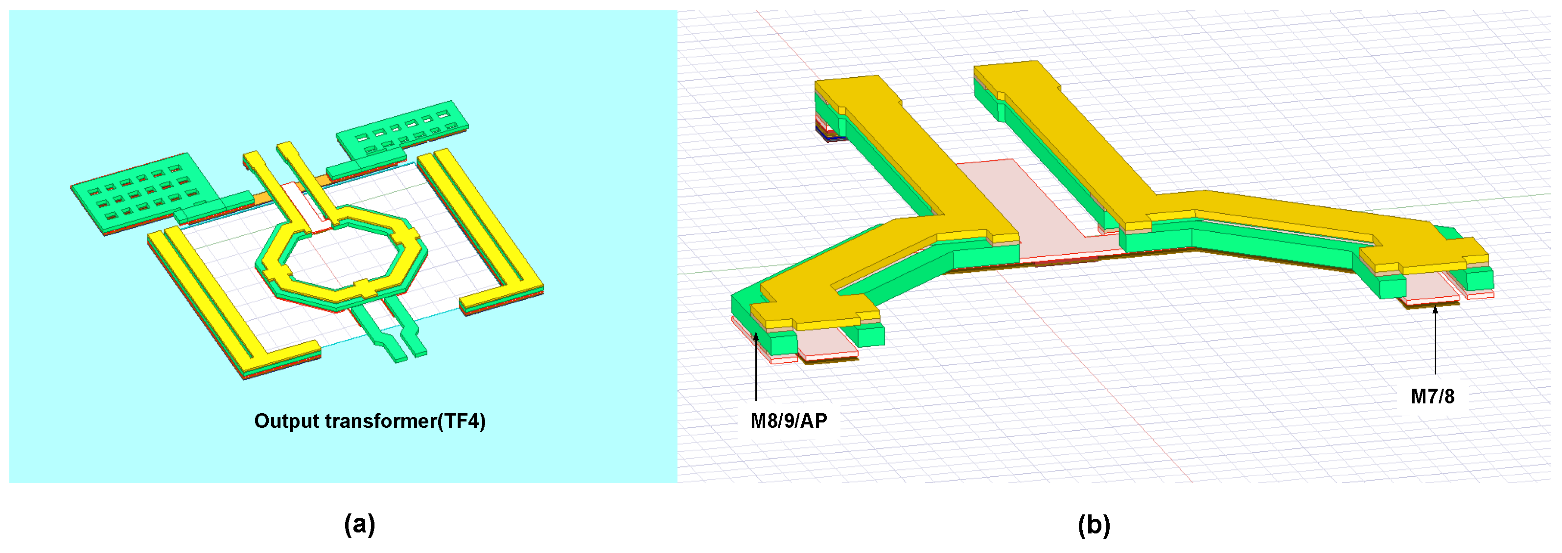
Assuming C 12 is 19 fF (could be changed in a later design stage if needed), then the total left capacitance C 1 = C 11 + C 12 is calculated to be 114.69 fF. An initial assumption of C 12 of 19 fF is based on the fact that there is usually parasitic capacitance of the transformer [16], and extra added capacitor C 12 can be used as an additional degree of freedom to facilitate the design of MCR. C 12 should be as small as possible because a larger C 12 (leading to a larger C 1 ) results in decreased GBW of the MCR [16]. According to Equations (6) and (7), Q = 1.0116, and k = 0.703 are obtained. According to Equations (8)–(10), we obtain that L 2 = L 1 = 303.26 pH, C 2 = C 1 = 114.69 fF, and C 22 = 25.69 fF at 32 GHz, respectively. Some iterations of the calculation and design tuning of the values of Q, k, L 1 , L 2 , and C 12 are necessary to make these parameters satisfy the no in-band ripple condition equations. Figure 4 presents (a) the 3D view of the output transformer (TF4 in Figure 1) in the symmetrical MCR and (b) its layer structure. To achieve a coupling factor k as high as 0.7, a combination of interleaved and stacked structures is employed [24,25,26], as shown in Figure 4b. The primary inductor of the stacked part is metal 8 paralleled with metal 7. The secondary inductor consists of metals 8 and 9 and the AP layer in parallel. These paralleled metals increase the Q factor of the windings. Also with a high k factor, according to Formula (11), the insertion loss of the transformer is decreased, in which η , Q p , Q s , and k represent the passive efficiency, the Q factor of primary/secondary windings, and the coupling coefficient of the two windings, respectively [5]. The distance between AP layer and metal 8 is as far as 4.94 μ m, so the parasitic capacitance between L 1 and L 2 is not high enough to affect the SRF of the output transformer seriously. Figure 5a,b show the finally realized inductance and Q factor of L 1 and L 2 . Figure 6a shows the k between L 1 and L 2 , and Figure 6b shows the 3D view of the whole output matching network, respectively.
η = 1 1 + 2 1 k 2 Q p Q s ( 1 + 1 k 2 Q p Q s ) + 2 k 2 Q p Q s
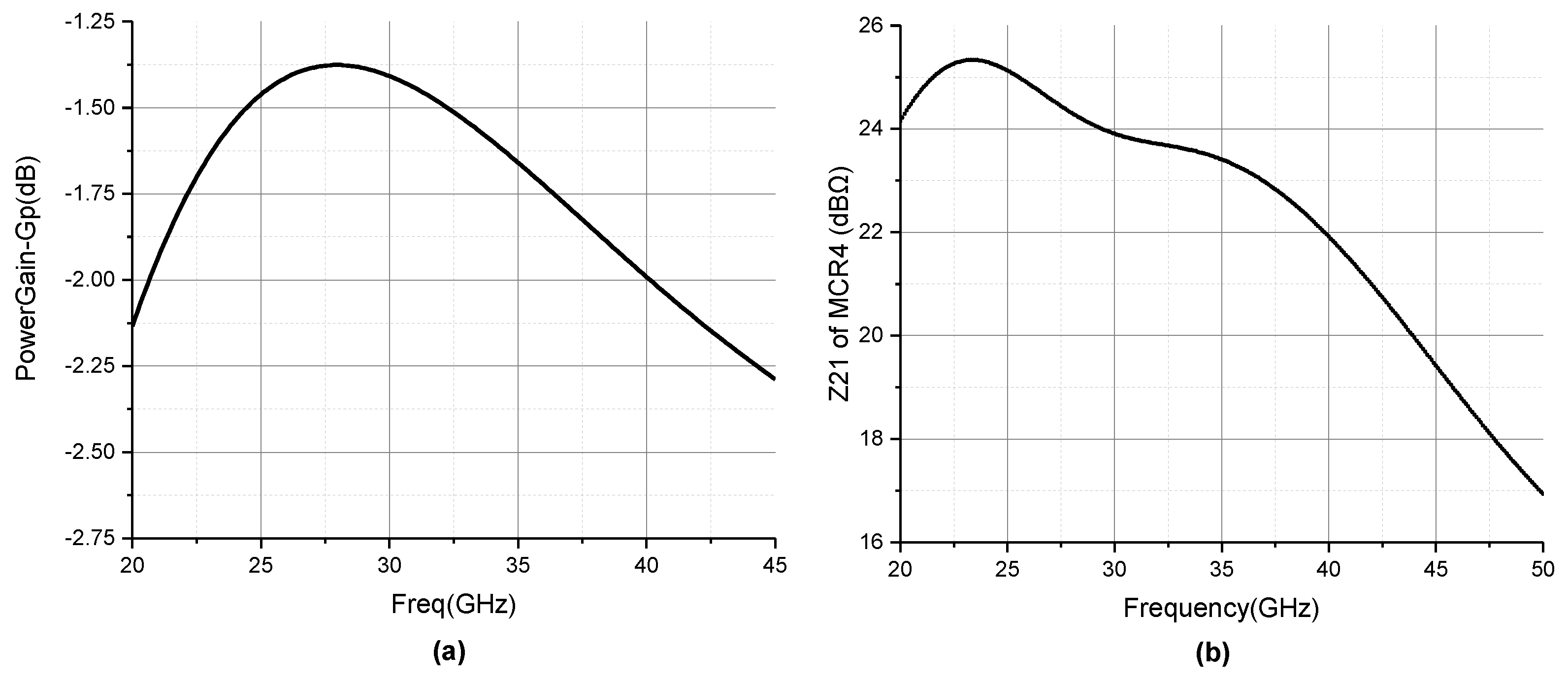
The power gain of the whole output matching network is presented in Figure 7a. The power gain is defined as [27]:
G p = P L P i n
in which P L represents the power delivered to the load, and P i n represents the power fed into the network. This factor takes into account the situation that the load impedance is not always matching [27]. The minimum loss is −1.376 dB at 28.1 GHz. In general, from 25 GHz to 40 GHz, the loss at high frequency is larger than that at low frequency. Figure 7b presents the trans-impedance (Z21) of the MCR4 with Z21 being defined as [28]:
Z 21 ( d B Ω ) = 20 l o g ( v 2 i 1 ) | i 2 = 0
in which v 2 , i 1 , and i 2 are defined in Figure 2. Compared with an ideal lossless symmetrical MCR, the finite Q parameter of the lossy transformer makes the two amplitude peaks of Z21 not equal anymore [29]. Also, the practical coupling factor k of a lossy transformer is not a constant value compared with an ideal transformer. The test schematic for the Z21 of MCR4 with a 50 Ω resistor at the input is shown in Figure 8. Although the input-matching condition of the power stage affects the test results, the power stage has good isolation due to the neutralization capacitors. Therefore, directly connecting a 50 Ω resistor at the power stage input does not have a significant impact on the test results of the Z21. Also, the test iteration for Z21 is needed when the matching passives are designed. As a result, the initial Z21 test result is used to provide an intuitive perception of the gain shape. With the matching network being placed in the circuit, the “in-situation” Z21 test method takes the circuit parasitics into account [20].
Figure 9a shows the power gain (Gp) of the power stage with the whole output matching network. From Figure 9a, we can see that the peak power gain at low frequency is much higher than that at high frequency, which has a similar trend as the Z21 shown in Figure 7b. Figure 9b presents a flattened input impedance of the output symmetrical MCR4 (including C 11 + C 12 of the power stage) over a wide frequency band, especially a wide band near zero imaginary part, which means that the capacitor ( C 11 + C 12 ) resonates with the right side impedance Z r i g h t shown in Figure 3, so that the drain of the output stage transistors can see a nearly pure real Ropt. The test circuit for the power stage with the whole output matching network is shown in Figure 10. With ideal LC input-matching networks at every single-frequency point, the large-signal performance of the power stage is tested from 26 GHz to 36 GHz and the results are shown in Figure 11a,b. For the large-signal performance, the power stage achieves a P s a t of 17.87 dBm at 31 GHz, a P A E m a x of 33.55% at 26 GHz, and a 14.4 dBm O P 1 d B at 31 GHz and 32 GHz. From Figure 11b, the simulated results reveal over a 17.3 dBm P s a t , over a 25% P A E m a x , and over a 13.8 dBm O P 1 d B from 26 to 36 GHz, which explains the wideband load–pull matching achieved by the whole output matching network.

2.2. Interstage Matching Network Design

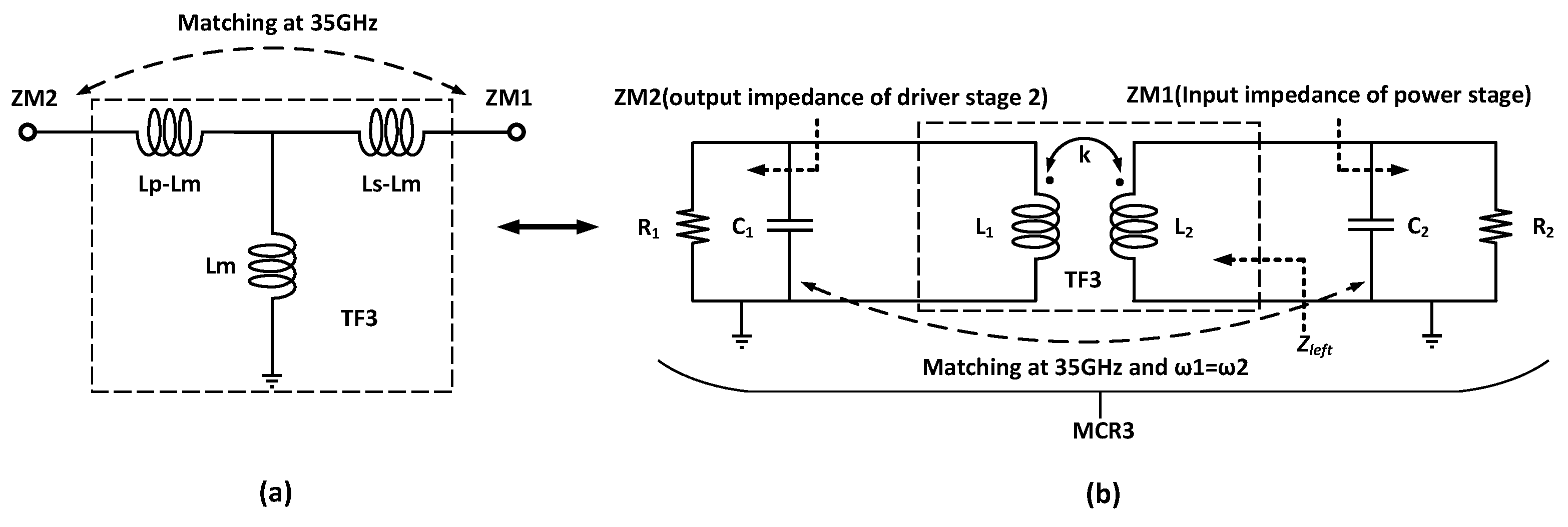
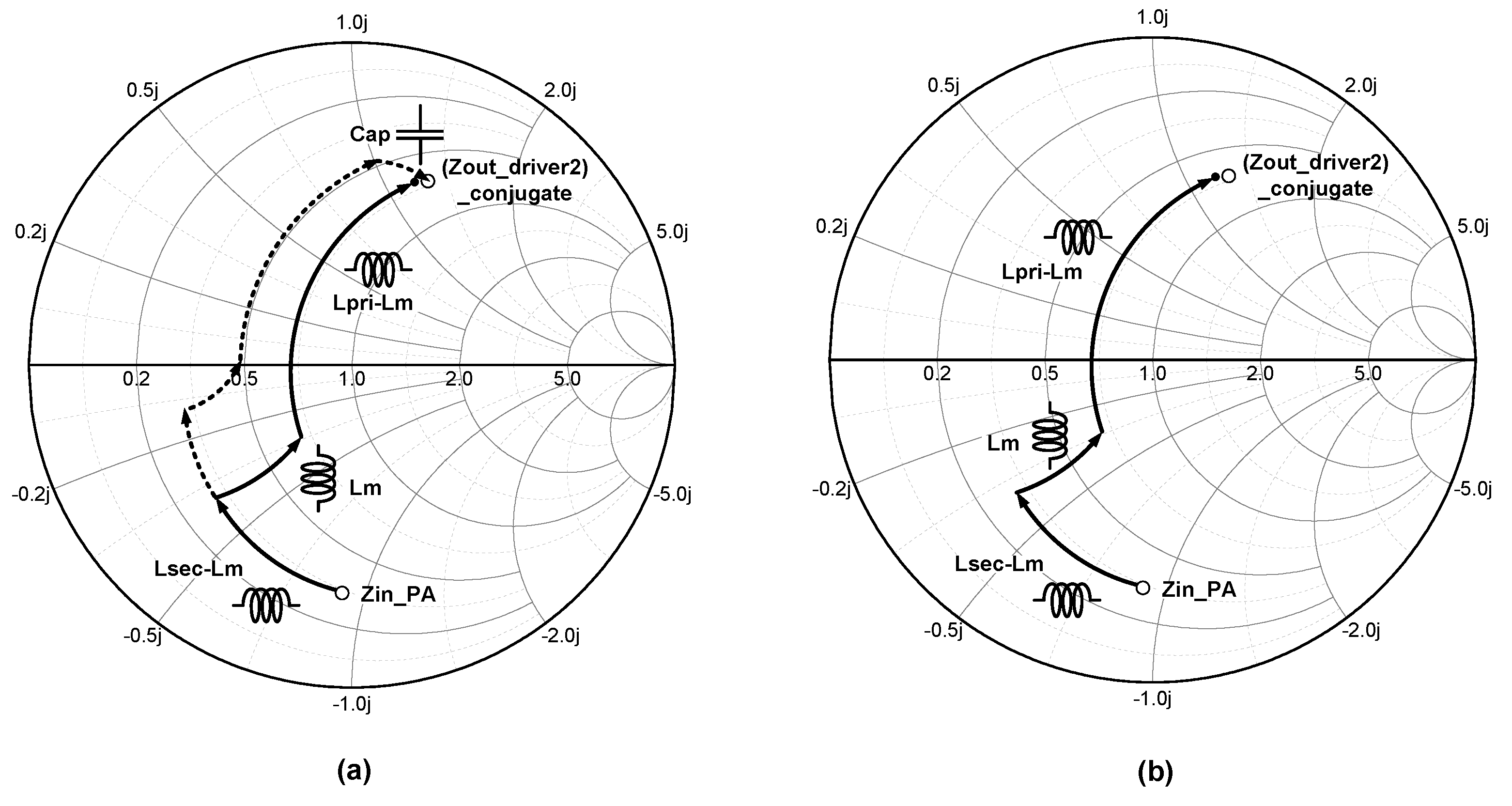
For the interstage matching network between the power stage and driver stage 2, the target is to achieve broadband matching between driver stage 2 output impedance and power stage input impedance. In transformer matching, we uses a simplified lumped T-model, shown in Figure 12, to estimate the size/parameters of the transformers [30]. For a transformer-based MCR, both the bandwidth and in-band ripple increase with higher coupling factor k, which has been investigated previously in references [16,31,32,33]. Meanwhile, the higher k results in lower insertion loss of the transformer. Considering that the TF1 and TF2 in MCR1 and MCR2 (shown in Figure 1) are used to adjust the small-signal bandwidth performance of the power amplifier, a higher k is preferred for TF3 (transformer 3 in MCR3 shown in Figure 1) regardless of the higher in-band ripple. Usually, the gate impedance has a higher Q factor than the output impedance of the transistor, and the higher Q results in increased gain ripple [16]. Adding paralleled resistors at the gate is an alternative way to reduce the Q factor and to extend the bandwidth [16,34]. Two 150 Ω resistors (Rg at the power stage) are added at the gate of the power stage. Then, the input impedance of the power stage after adding resistors at the gate is ZM1 = 16 − j*43.6. The output impedance of driver stage 2 is ZM2 = 33.56 − j*62.78. The equivalent T matching of TF3 and the specific structure of MCR3 are shown in Figure 13a,b, respectively. In the MCR3, the output impedance of diver stage 2 (ZM2) is equivalent to a paralleled tank including a resistor R 1 and a capacitor C 1 . The input impedance of the power stage (ZM1) is equivalent to a paralleled tank including a resistor R 2 and a capacitor C 2 . The ZM2 is affected by the input-matching condition of driver stage 2 due to the non-zero S12 of the transistors. Considering that the neutralization technique is used for all three stages to cancel out the effect of Cgd of the transistors, the S12 for all three stages is small enough so that the ZM2 of driver stage 2 is not severely affected by the previous matching condition. Also, simulation iterations can be set to reset the value of ZM2. The TF3 is used to match ZM1 and ZM2. According to reference [35], when the two resonators of an MCR satisfy the condition of ω 1 = ω 2 , the peak Z21 of an asymmetrical MCR is almost the same as that of a symmetrical MCR, and the mismatch of ω 1 and ω 2 will deteriorate the insertion loss, especially at a higher frequency. In MCR3, Q 1 = 1.87 and Q 2 = 2.725 are obtained at 35 GHz. With a lower Q 1 and ω 1 = ω 2 , the MCR3 achieve a better flat response and the mismatch of Q 1 and Q 2 could be accepted [35]. With the help of TF3, the matching between ZM1 and ZM2 has lots of matching trajectories, only including the T-model or T-model with extra capacitors, as shown in Figure 14a. Considering that the gain and output power of the transistors decrease as the operating frequency increases, the matching trajectory of TF3 is designed to achieve a good match at 35 GHz, and also ω 1 = ω 2 is set at 35 GHz, as shown in Figure 14b. Thus, a good match between ZM1 and ZM2 at 35 GHz and ω 1 = ω 2 for a better flat response are both satisfied for MCR3. Figure 15 presents the 3D view of the practical designed TF3. For the finally realized TF3, L1 is 561.46 pH and L2 is 348.62 pH with k being 0.525 at 35 GHz. Figure 16a presents the matching situation between power stage input impedance (ZM1) and Z l e f t (shown in Figure 13b) from 26 GHz to 36 GHz. A good match (S11 below −11 dB) between ZM1 and Z l e f t is achieved from 26 GHz to 36 GHz. Figure 16b shows the Z21 of MCR3 (TF3 is included) with the similar test method of MCR4 mentioned above. In Figure 16b, the Z21 magnitude at low frequency (25–30 GHz) is higher than that at higher frequency (35–40 GHz).
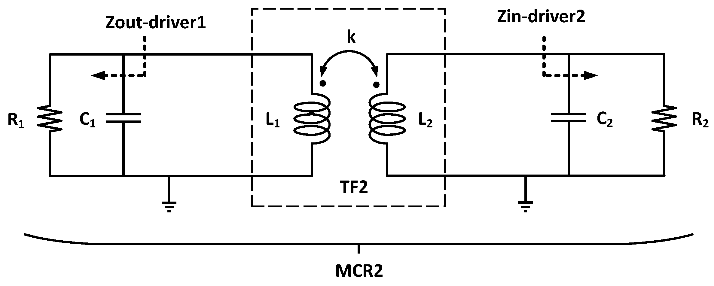
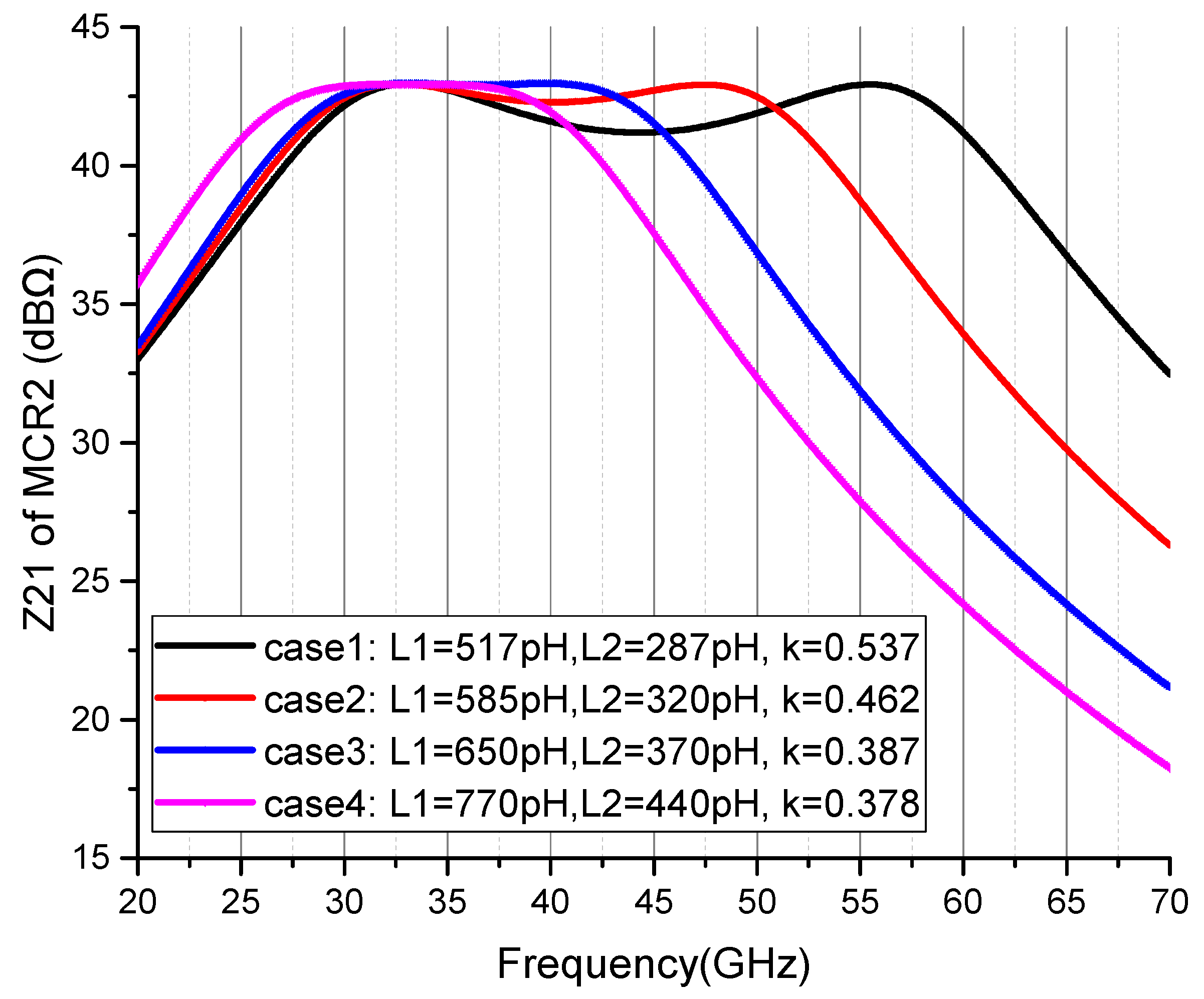
For the interstage matching network between driver stage 1 and driver stage 2, which is part of MCR2, it aims to achieve a high-pass form Z21 to compensate for the gain drop in MCR3 and MCR4 at high frequency. To achieve the high-pass form Z21, 33 GHz is selected as the initial matching frequency point between the input impedance of driver stage 2 (Zin-diver2) and the output impedance of driver stage 1 (Zout-driver1). At 33 GHz, Zin-driver2 = 30.62 − j*72.94 and Zout-driver1 = 50.48 − j*130.14, which is equivalent to parallel R and C of (204.37 Ω ||56.21 fF) and (385.99 Ω ||32.21 fF), respectively, as shown in Figure 17. Actually, there are lots of alternative transformers with different parameter combinations to match Zin-driver2 and Zout-driver1 at 33 GHz. The frequency points of the two peaks of Z21 for an MCR are affected by 1 L 1 C 1 , 1 L 2 C 2 , and the coupling coefficient k [36]. Thus, the peak Z21 positions for MCR2 is adjusted by tuning these parameters. Figure 18 presents a group of Z21 lines with different L 1 , L 2 , and k. In all four cases, Zin-driver2 and Zout-driver1 are conjugate-matched at 33 GHz. In Figure 18, different parameter combinations of the transformers have different peak Z21 positions and different in-band ripples, resulting in different Z21 gain shapes with matching networks inserted in the amplifier. A combination of L 1 = 585 pH, L 2 = 320 pH, and k = 0.462 (red line in Figure 18) is selected for TF2 to achieve the high-pass Z21 shape of MCR2. The two Z21 peaks are located at 32.5 GHz and 47.5 GHz, respectively, as shown in Figure 18. Figure 19a presents the 3D view of transformer 2 (TF2) in MCR2. Figure 19b shows the Z21 of MCR2 with a similar test method to those of MCR3 and MCR4, as mentioned above, by using the EM simulation result of TF2. Like the cases in MCR4 and MCR3, a finite Q of the inductors makes the Z21 line of MCR2 different from that using an ideal transformer (red line in Figure 18). However, the average magnitude of the Z21 from 32.5 GHz to 40 GHz is relatively higher than that from 25 GHz to 32.5 GHz. Therefore, it indicates that a high-pass form Z21 is achieved.

2.3. Input-Matching Network Design

For the input-matching network, an asymmetrical MCR1 satisfying ω 1 / ω 2 = Q 1 / Q 2 and resulting in two equal Z21 peaks, is used to extend the bandwidth [16]. Figure 20a presents the lumped model of MCR1 based on TF1 for matching. The input impedance of the input stage (ZM1 = 42.94 − j*119 at 36 GHz) is equivalent to a paralleled tank including a resistor R 2 and a capacitor C 2 . The output impedance of the power splitter (ZM2 = 82.16 − j*22.12 at 26 GHz) is equivalent to a paralleled tank including a resistor R 1 and a capacitor C 11 . The power splitter is designed by using microstrip transmission-line segments to reactively match the impedance and split the input power to the two-way driver stage 1 in-phase, as shown in Figure 20b. C 12 on the left side is the extra added capacitor to satisfy the condition of ω 1 / ω 2 = Q 1 / Q 2 for the asymmetrical MCR1. In MCR1, we set ω 1 = 26 GHz, ω 2 = 36 GHz. For the input stage, as shown in Figure 1, a pair of paralleled Rg of 500 Ω , and a pair of series Rs of 10 Ω are added at the gate of the input transistors. All these resistors decrease the Q factor of the input impedance of the transistors. Also, Rs improves the common mode stability of the circuit. After adding these resistors, the input impedance of the input stage ZM1 is 42.94 − j*119 at 36 GHz. Its equivalent paralleled resistance and capacitance are R 2 = 372.7 Ω and C 2 = 32.87 fF, respectively. As L 2 resonates with C 2 at 36 GHz, we obtain L 2 = 1 ω 2 2 C 2 = 594.6 pH and Q 2 = ω 2 * R 2 C 2 = 2.771. Based on ω 1 / ω 2 = Q 1 / Q 2 , we obtain Q 1 = 2 and C 1 = 139 fF. As L 1 resonates with C 1 at 26 GHz, we acquire L 1 = 1 ω 1 2 C 1 = 269.5 pH. As mentioned above, C 11 is the equivalent output paralleled capacitor of the power splitter, which is 18.7 fF at 26 GHz in this work; thus, the added extra capacitor C 12 is 120.33 fF (equals to ( C 1 C 11 )). So far, the coupling factor k between L 1 and L 2 has not been determined. Usually, a higher k makes the two Z21 magnitude peaks of an MCR be apart from each other [16,31,32,33]. Figure 21 shows the Z21 of the MCR1 with a k increasing from 0.3 to 0.7, when the inductors and capacitors are all ideal components. With an increasing k, both the bandwidth and in-band ripple are increased. Considering the target frequency, in-band ripple, and the difficulties of an actual transformer implementation, a k of 0.573 at 32 GHz is selected and achieved for this MCR1. The 3D view of the input transformer (TF1) is shown in Figure 20b. The primary inductance ( L 1 ) at 26 GHz is 266.65 pH, and the secondary inductance ( L 2 ) is 596.4 pH at 36 GHz for the finally achieved practical transformer.
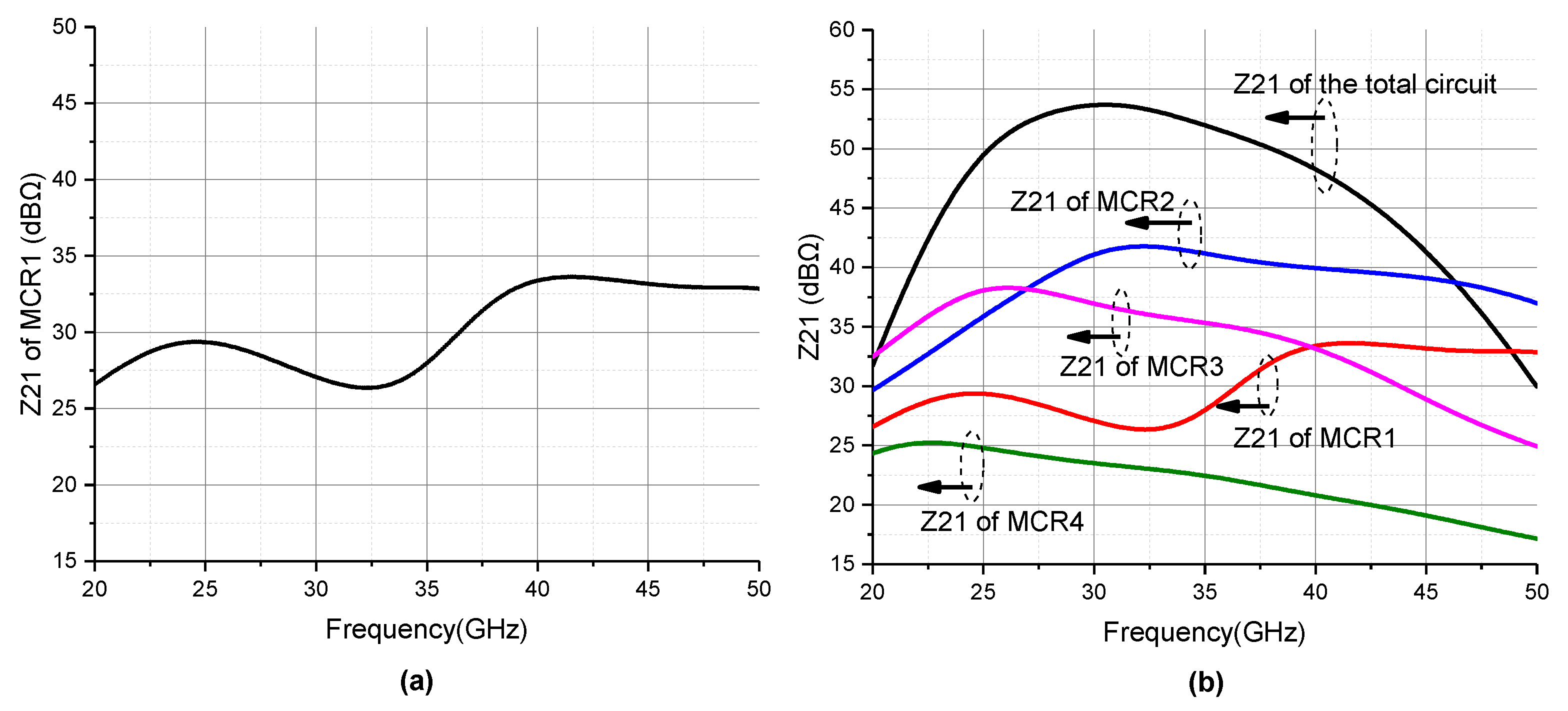
Figure 22a presents the Z21 of MCR1 with the whole input-matching network shown in Figure 20b. Compared with the initial desire with the condition of ω 1 / ω 2 = Q 1 / Q 2 , the two Z21 peaks are not equal anymore. The loss of the transformer affects the Z21 response [29]. Meanwhile, the equivalent R 1 , R 2 , L 1 , L 2 , and k being non-constant with frequency also affects the Z21 response. In Figure 22a, the Z21 magnitude of MCR1 at the frequency edge (from 25 GHz to 40 GHz) is much higher than that at the frequency center (from 30 GHz to 35 GHz). Therefore, the Z21 drop at the band edge is compensated, like the case in reference [7]. Figure 22b presents the Z21 of each MCR and the Z21 of the total circuit. It indicates that the Z21 amplitudes of the first and second MCRs compensate for that of the third and the fourth. Therefore, a wideband total Z21 of the whole circuit from input to output is achieved.

3. The PA Circuit Implementation

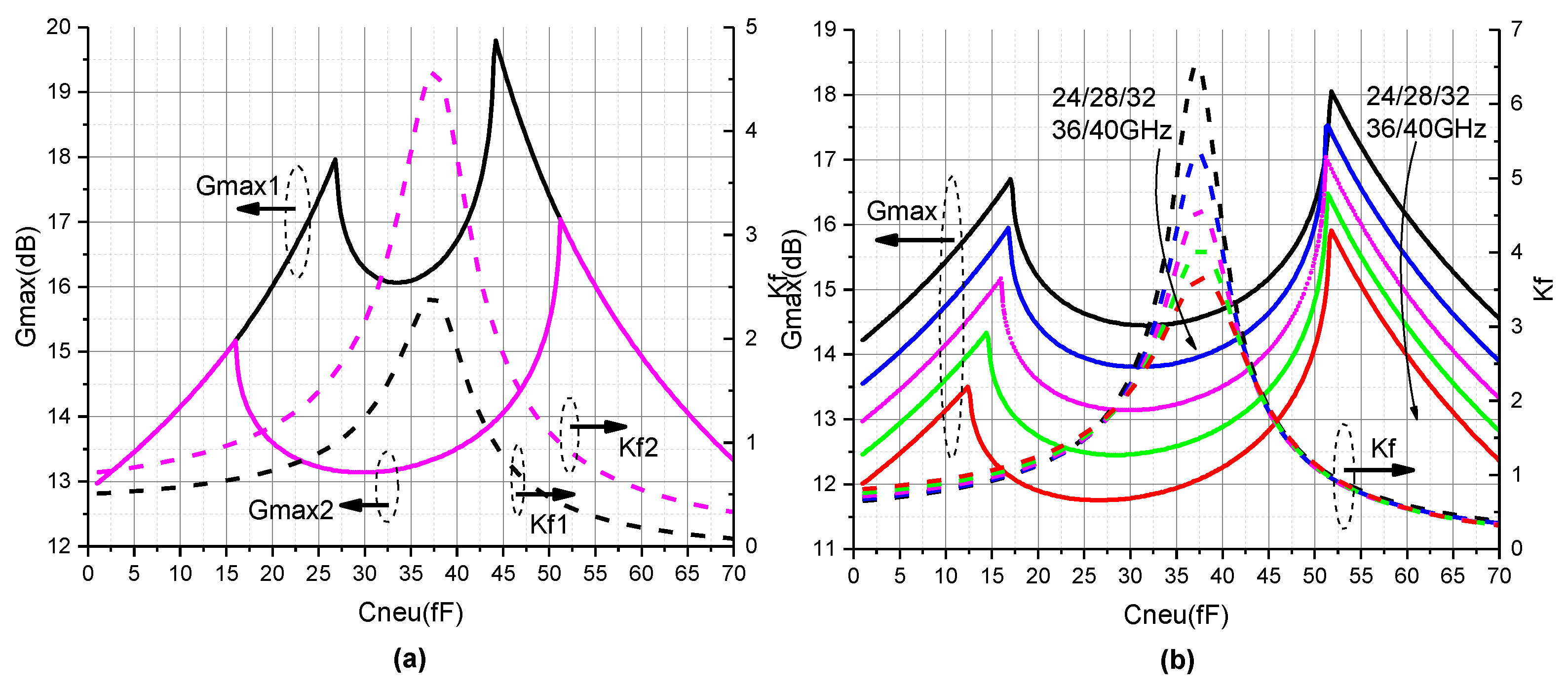
Figure 1 shows the architecture of the implemented wideband power amplifier. Three common-source stages are used to improve power gain and to stagger the Z21 of each MCR stage conveniently. Output power is increased by two-way current-combining. The matching networks mainly consist of transformer-based MCRs between each stage and transmission lines for the input and output. The gate biases of the transistors are supplied through the center tap of the transformers (TF1, TF2, and TF3) by series resistors (R1) of 250 Ω to improve common mode stability [37]. Especially for the input stage, series resistors Rs of 10 Ω are inserted between gate and the input transformer (TF1) to further suppress the common-mode oscillation. Pseudo-differential NMOS pair with neutralization capacitors has been employed to all the stages. The neutralization capacitors implemented via metal–oxide–metal are used to tackle the negative feedback and to improve reverse isolation [37]. Then, both the power gain and stability are improved. Shunt resistors are added at the gate of each stage to reduce the Q factor of the impedance, to help implement matching, and also to improve the stability of the circuit. Figure 23a presents the Gmax and stability of the 128 μ m transistor used in the output differential pair versus the values of neutralization capacitance (Cneu) at 32 GHz. Gmax1 and Kf1 present the condition without gate paralleled resistors, and Gmax2 and Kf2 present the condition that two 150 Ω gate paralleled resistors (Rg for output stage) are added. It indicates that the Cneu range sustaining Kf > 1 is extended from about 23.9% to 51.7%. Also, the Gmax decreases by about 3 dB when Cneu is 37 fF. Considering that the whole circuit is composed of three cascaded circuit stages, the gain reduction induced by these shunt resistors at each stage is acceptable. Figure 23b shows the Gmax and Kf at different frequencies with shunt resistors added. It demonstrates that the Cneu ranges sustaining Kf > 1 at different frequencies are almost the same. Even at 40 GHz, the Gmax is bigger than 11.75 dB. The neutralization capacitance (Cneu) selected for the three stages are 37 fF/17 fF/9.5 fF, respectively. All the neutralization capacitors are implemented with parallel-plate metals. In this work, 2*32/1*32/1*16 fingers with a finger width of 2 µm (128 μ m*2 for the output stage differential pair) for the output stage, driver stage 2, and driver stage 1 are used for better performance. The metal lines on transistors are simulated using a 3D EM simulator. The 1.1 V VDD supply is fed through the center tap of the transformers. The 0.6 V VGS for the power stage and driver stage 2 and 0.55 V for driver stage 1 are selected for the consideration of output power and PAE.

4. Results and Discussion

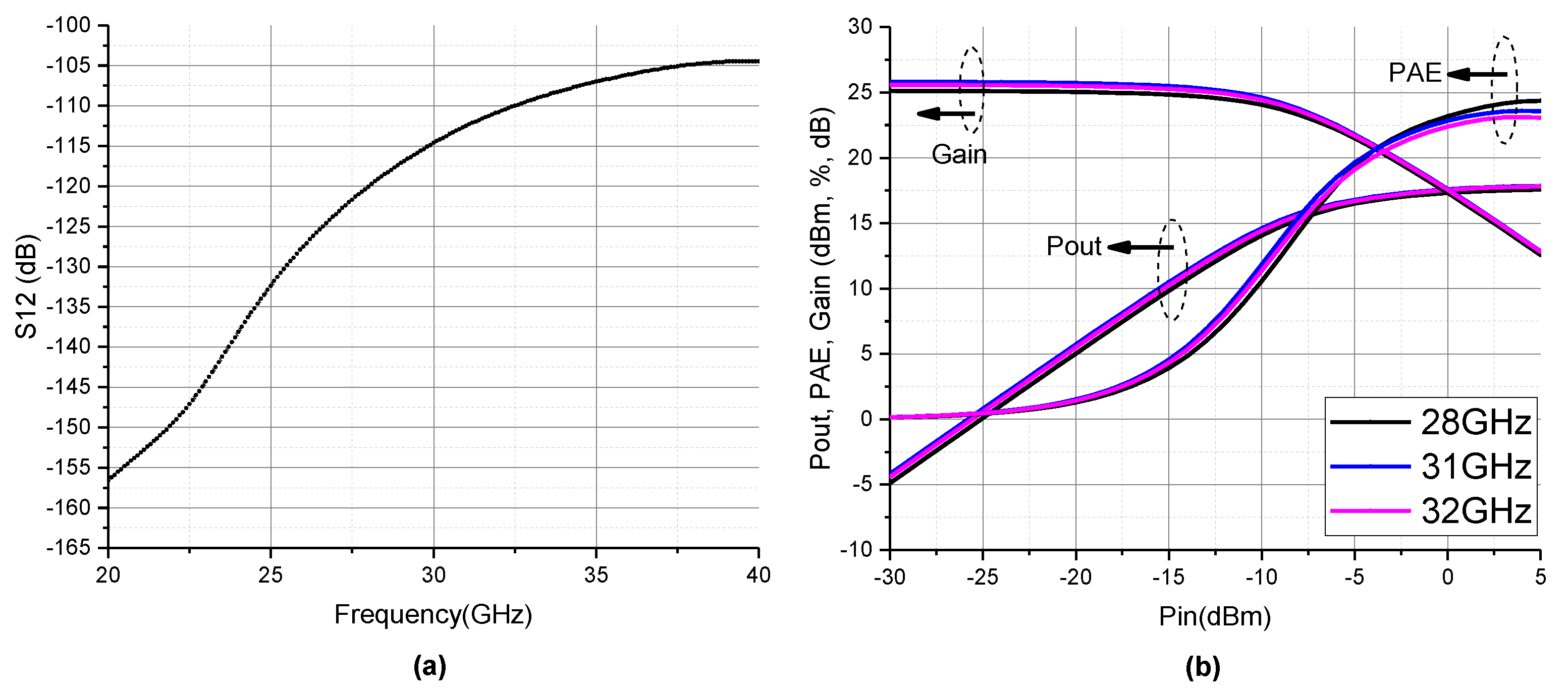
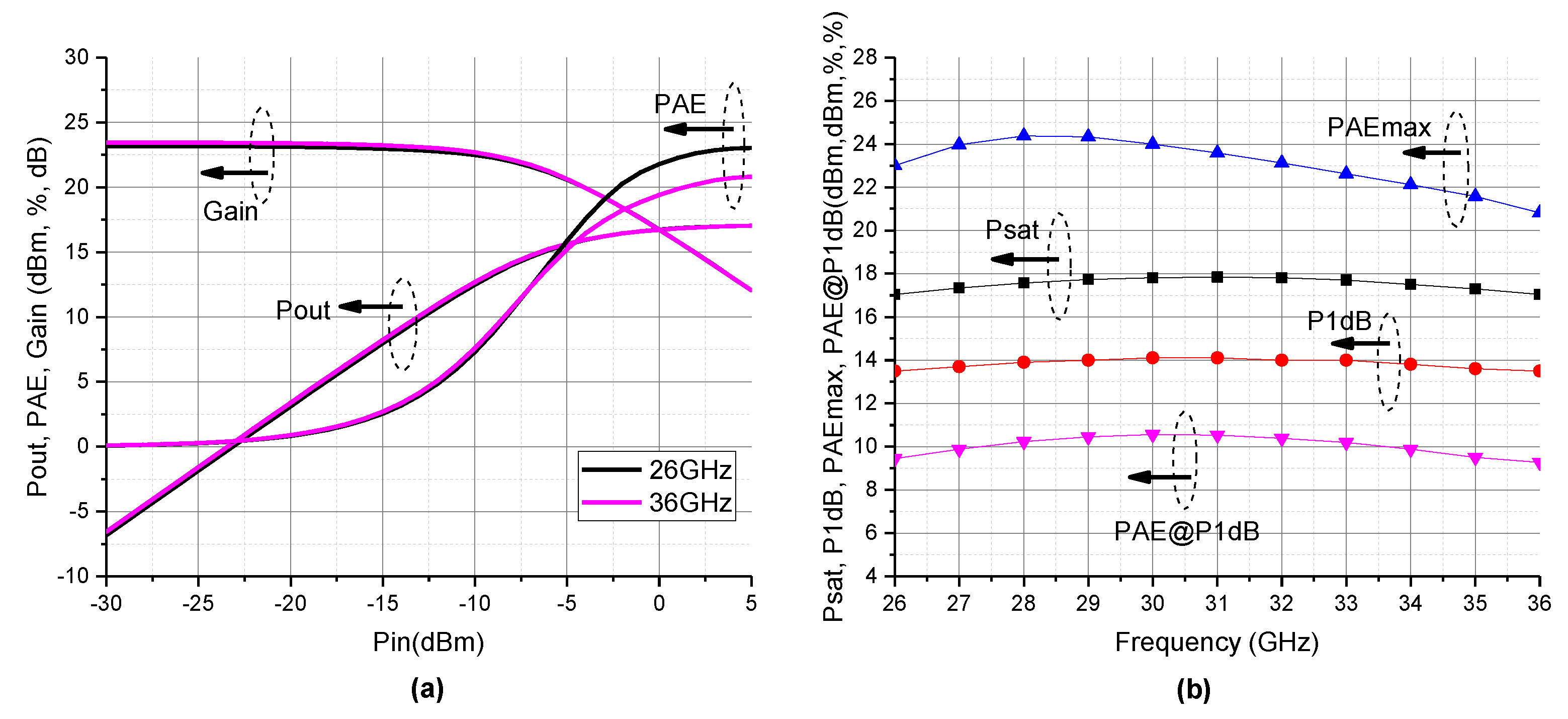
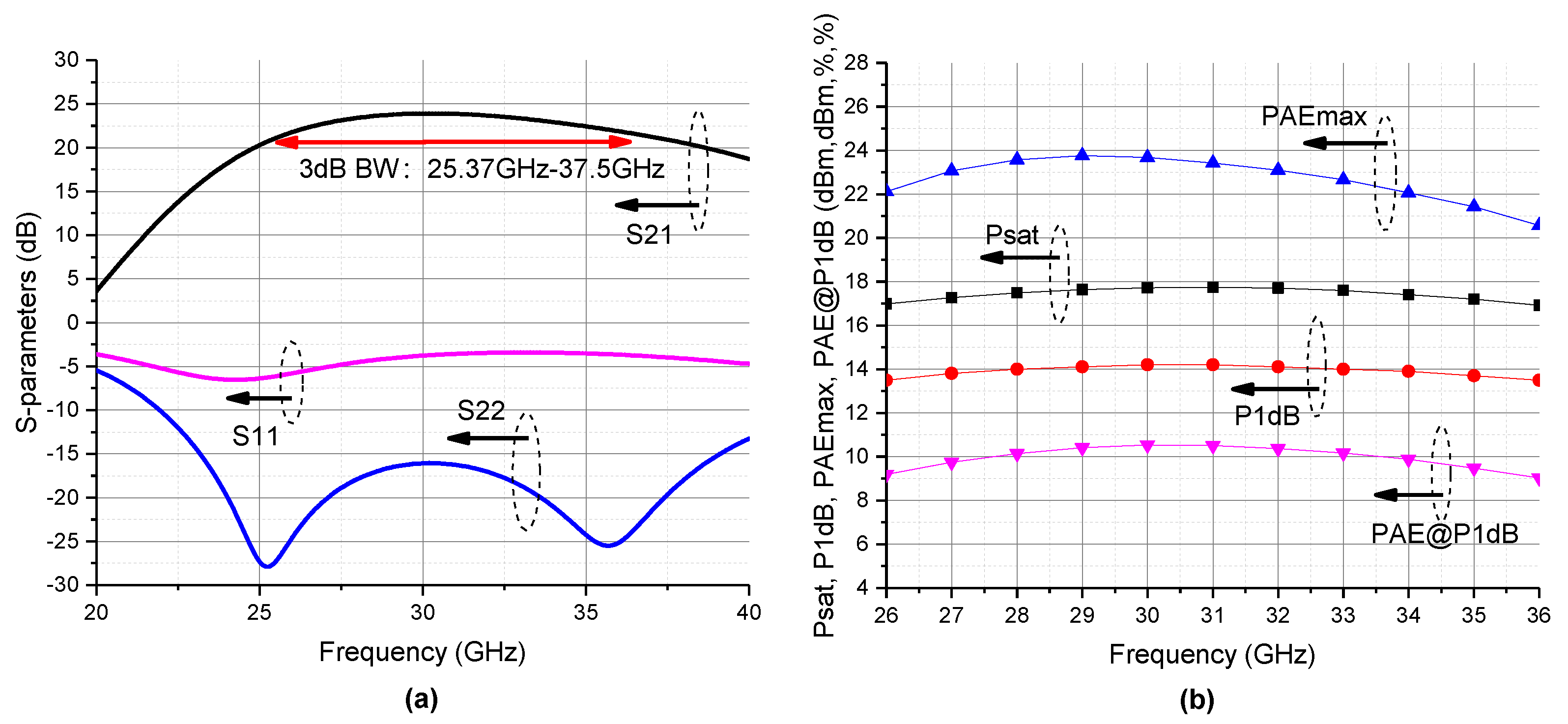
A wideband power amplifier is designed in 65 nm CMOS technology and the layout is shown in Figure 24a. The area of the chip core is about 0.686 mm*1.933 mm. Figure 24b presents the simulated S-parameters of the designed power amplifier. The peak small-signal gain is 25.87 dB at 35.5 GHz, with a 3 dB bandwidth of 11.1 GHz from 25.8 GHz to 36.9 GHz. The output reflection coefficient is lower than −10 dB from 22 GHz to 43.5 GHz while the worst input reflection coefficient is only lower than −3 dB as the design goal is to broaden the bandwidth of the gain rather than wideband input matching at the input. Benefiting from the multiple-neutralization-stage design, the reverse isolation is better than −100 dB from 20 GHz to 40 GHz, as shown in Figure 25a. The stability factor Kf is greater than 1000 for all the frequencies. The large-signal performance versus input power (Pin) at 28/31/32 GHz is shown in Figure 25b. Biased at 1.1 V supply voltages for all the three stages, the power amplifier achieves a P s a t of 17.57 dBm/17.84 dBm/17.81 dBm, a P A E m a x of 24.37%/23.59%/23.12%, a O P 1 d B of 13.92 dBm/14.09 dBm/14.04 dBm, and a P A E P 1 d B of 10.24%/10.53%/10.38% at 28/31/32 GHz, respectively. Also, as shown in Figure 26a, at the frequency edge of interest, i.e., 26 GHz and 36 GHz, a P s a t of 17.04 dBm/17.04 dBm, an O P 1 d B of 13.54 dBm/13.47 dBm, a P A E m a x of 23%/20.81%, and a P A E P 1 d B of 9.45%/9.27% are achieved, respectively. To check the wideband large-signal performance of the designed power amplifier, Figure 26b presents the P s a t , O P 1 d B , P A E m a x , and P A E P 1 d B from 26 GHz to 36 GHz. The designed power amplifier achieves a P s a t of 17.44 ± 0.4 dBm with a P A E m a x of 22.59 ± 1.78%, and an O P 1 d B of 13.78 ± 0.31 dBm under the 1.1 V supply voltage. Compared with the results of the only power stage with ideal LC input matching in Figure 11b, the average P s a t and O P 1 d B deteriorate from 17.66 dBm and 14.21 dBm to 17.52 dBm and 13.85 dBm from 26 GHz to 36 GHz, respectively. The average P A E m a x decreases from 29.46% to 23.04%. The results prove that the designed power amplifier achieves wideband performances in both small- and large-signal performance using the wideband output symmetrical MCR and the staggered MCRs between stages. Table 1 summarizes the performance of the designed wideband power amplifier and compares it with other state-of-the-art PAs in the Ka-band. Our power amplifier demonstrates the highest gain compared with the previous work in Table 1 despite the use of staggering. Both the small- and large-signal bandwidths are competitive among the references in Table 1 besides the FD-SOI power amplifier in reference [29]. With a 1.1 V VDD supply and the power combining method, the P s a t and O P 1 d B of our power amplifier are impressive besides the work with a 3.3 V/2.2 V supply in references [23,38], respectively. Figure 27 and Figure 28 present the S-parameters and large-signal performance at the ff corner and ss corner, respectively. At both the ff corner and ss corner, the DC bias current of all the stages is adjusted by changing the gate bias voltage to make it nearly the same as that at the tt corner. At the ff corner, the 3 dB small-signal bandwidth is 12.13 GHz, with a peak gain of 23.9 dB, as shown in Figure 27a. It achieves a flat P s a t of 16.91–17.74 dBm, a flat O P 1 d B of 13.51–14.17 dBm, and a P A E m a x of 20.57–23.76%, between 26 GHz and 36 GHz, at the ff corner. At the ss corner, the 3 dB small-signal bandwidth is 10.29 GHz, with a peak gain of 27.57 dB, as shown in Figure 28a. In Figure 28b, the power amplifier achieves a flat P s a t of 17.08–17.87 dBm, a flat O P 1 d B of 13.22–13.88 dBm, and a P A E m a x of 20.72–24.7%, between 26 GHz and 36 GHz. These results indicate that the broadband characteristics of the designed power amplifier are relatively stable.

5. Conclusions

This article presents a wideband power amplifier in 65nm CMOS covering the bandwidth from 25.8 GHz to 36.9 GHz. A symmetrical output MCR is designed to achieve wideband optimum load impedance for the power amplifier. To flatten the small-signal bandwidth of the power amplifier, staggered interstage and input MCRs are custom-designed. A high-pass form MCR2 and an asymmetrical MCR1 satisfying ω 1 / ω 2 = Q 1 / Q 2 are used to successfully compensate and stagger the Z21 shape of MCR3 and MCR4. To increase the output power, the two-way current combining method is used via a microstrip transmission line power combiner and splitter. Three common-source stages with neutralization capacitors are used to improve power gain and stability and to stagger the Z21 of each MCR conveniently. Benefiting from the above-mentioned design considerations, the power amplifier achieves both wideband small- and large-signal performance. A peak small-signal gain of 25.87 dB with 3 dB bandwidth from 25.8 GHz to 36.9 GHz is achieved. From 26 GH to 36 GHz, a P s a t of 17.44 ± 0.4 dBm with a 22.59 ± 1.78% P A E m a x and an O P 1 d B of 13.78 ± 0.31 dBm under the 1.1 V supply voltage are realized. These results indicate that this power amplifier is competitive on the applications of wideband millimeter-wave communication.

Author Contributions

Conceptuation, Z.W.; methodology, Z.W.; validation, Z.W.; software, Z.W. and X.W.; formal analysis, Z.W.; investigation, Z.W.; writing—original draft preparation, Z.W.; writing—review and editing, Z.W., X.W. and Y.L.; project administration X.W. and Y.L. All authors have read and agreed to the published version of the manuscript.

Funding

This work was supported by National Natural Science Foundation of China under grant 61574165.

Data Availability Statement

Not applicable.

Conflicts of Interest

The authors declare no conflict of interest.

References

  1. Zhao, C.; Zhang, X.; Liu, H.; Yu, Y.; Wu, Y.; Kang, K. A SiGe Power Amplifier with Double Gain Peaks Based on the Control of Stationary Points of Impedance Transformation. IEEE Trans. Microw. Theory Tech. 2021, 69, 2279–2290. [Google Scholar] [CrossRef]
  2. Cheng, D.; Chen, X.; Chen, Q.; Li, L.; Sheng, B. Design of an Ultra-Compact 60-GHz Bi-Directional Amplifier in 65-nm CMOS. IEEE Microw. Wirel. Components Lett. 2022, 32, 343–346. [Google Scholar] [CrossRef]
  3. 3GPP 5G-NR Specifications. Available online: http://www.3gpp.org/DynaReport/38-series.htm> (accessed on 15 August 2019).
  4. Federal Communications Commission FCC 16–89. Available online: https://docs.fcc.gov/public/attachments/FCC-16-89A1.pdf (accessed on 15 August 2019).
  5. Wang, F.; Wang, H. A Broadband Linear Ultra-Compact mm-Wave Power Amplifier With Distributed-Balun Output Network: Analysis and Design. IEEE J. Solid State Circuits 2021, 56, 2308–2323. [Google Scholar] [CrossRef]
  6. Wang, F.; Wang, A.; Wang, H. A 22–37 GHz Broadband Compact Linear Mm-Wave Power Amplifier Supporting 64-/256-/512-QAM Modulations for 5G Communications. In Proceedings of the 2020 IEEE/MTT-S International Microwave Symposium (IMS), Los Angeles, CA, USA, 4–6 August 2020; pp. 1105–1108. [Google Scholar] [CrossRef]
  7. Wang, D.; Shen, Z.; Su, X.; Liu, Z.; Tan, Y.; Xu, C.; Liu, J.; Liao, H. A Gm-Compensated 46–101 GHz Broadband Power Amplifier for High-Resolution FMCW Radars. In Proceedings of the 2021 IEEE International Symposium on Circuits and Systems (ISCAS), Daegu, Republic of Korea, 22–28 May 2021; pp. 1–5. [Google Scholar] [CrossRef]
  8. Mostajeran, A.; Naghavi, S.M.; Emadi, M.; Samala, S.; Ginsburg, B.P.; Aseeri, M.; Afshari, E. A High-Resolution 220-GHz Ultra-Wideband Fully Integrated ISAR Imaging System. IEEE Trans. Microw. Theory Tech. 2019, 67, 429–442. [Google Scholar] [CrossRef]
  9. Wu, H.F.; Cheng, Q.F.; Li, X.G.; Fu, H.P. Analysis and Design of an UltraBroadband Stacked Power Amplifier in CMOS Technology. IEEE Trans. Circuits Syst. II Express Briefs 2016, 63, 49–53. [Google Scholar] [CrossRef]
  10. Thayyil, M.V.; Li, S.; Joram, N.; Ellinger, F. A 4–32 GHz SiGe Multi-Octave Power Amplifier with 20 dBm Peak Power, 18.6 dB Peak Gain and 156. IEEE Microw. Wirel. Components Lett. 2019, 29, 745–748. [Google Scholar] [CrossRef]
  11. Lin, J.; Li, L.; Huang, J. A Design of Full Ka-Band Power Amplifier in 65 nm SOI CMOS. In Proceedings of the 2022 7th International Conference on Integrated Circuits and Microsystems (ICICM), Xi’an, China, 28–31 October 2022; pp. 295–298. [Google Scholar] [CrossRef]
  12. Arbabian, A.; Niknejad, A.M. Design of a CMOS Tapered Cascaded Multistage Distributed Amplifier. IEEE Trans. Microw. Theory Tech. 2009, 57, 938–947. [Google Scholar] [CrossRef]
  13. El-Aassar, O.; Rebeiz, G.M. A DC-to-108-GHz CMOS SOI Distributed Power Amplifier and Modulator Driver Leveraging Multi-Drive Complementary Stacked Cells. IEEE J. Solid State Circuits 2019, 54, 3437–3451. [Google Scholar] [CrossRef]
  14. Mosalam, H.; Allam, A.; Jia, H.; Abdel-Rahman, A.B.; Pokharel, R.K. High Efficiency and Small Group Delay Variations 0.18- μ m CMOS UWB Power Amplifier. IEEE Trans. Circuits Syst. II Express Briefs 2019, 66, 592–596. [Google Scholar] [CrossRef]
  15. Hadipour, K.; Ghilioni, A.; Mazzanti, A.; Bassi, M.; Svelto, F. A 40 GHz to 67 GHz bandwidth 23 dB gain 5.8 dB maximum NF mm-Wave LNA in 28 nm CMOS. In Proceedings of the 2015 IEEE Radio Frequency Integrated Circuits Symposium (RFIC), Phoenix, AZ, USA, 17–19 May 2015; pp. 327–330. [Google Scholar] [CrossRef]
  16. Jia, H.; Prawoto, C.C.; Chi, B.; Wang, Z.; Yue, C.P. A Full Ka-Band Power Amplifier with 32.965-nm CMOS. IEEE Trans. Circuits Syst. Regul. Pap. 2018, 65, 2657–2668. [Google Scholar] [CrossRef]
  17. Wan, C.; Zhang, H.; Zhao, Y.; Zeng, M.; Dong, J.; Li, L.; Wang, K. A Broadband SiGe HBT Cascode Power Amplifier Achieving Watt-Level Peak Output Power with 38.6. IEEE Trans. Circuits Syst. II Express Briefs 2022, 69, 4734–4738. [Google Scholar] [CrossRef]
  18. Wei, D.; Wu, T.; Ma, S.; Chen, Y.; Ren, J. A 35-to-50 GHz CMOS Low-Noise Amplifier with 22.2 Bandwidth and 30.5-dB Maximum Gain for 5G New Radio. In Proceedings of the ESSCIRC 2021—IEEE 47th European Solid State Circuits Conference (ESSCIRC), Online, 6 September–30 November 2021; pp. 195–198. [Google Scholar] [CrossRef]
  19. Chou, C.F.; Hsiao, Y.H.; Wu, Y.C.; Lin, Y.H.; Wu, C.W.; Wang, H. Design of a V-Band 20-dBm Wideband Power Amplifier Using Transformer-Based Radial Power Combining in 90-nm CMOS. IEEE Trans. Microw. Theory Tech. 2016, 64, 4545–4560. [Google Scholar] [CrossRef]
  20. Xue, Y.; Shi, C.; Chen, G.; Chen, J.; Zhang, R. Two W-Band Wideband CMOS mmW PAs for Automotive Radar Transceivers. In Proceedings of the 2020 IEEE/MTT-S International Microwave Symposium (IMS), Los Angeles, CA, USA, 4–6 August 2020; pp. 1109–1112. [Google Scholar] [CrossRef]
  21. Zhang, R.; Xue, Y.; Jiang, C.; Shi, C.; Chen, G. Two High Power and Broadband Power Amplifiers using Transformer-based Resonating Peak Control Technique for E-Band Communication and Automotive Radars in 55-nm CMOS. In Proceedings of the 2020 International Conference on Microwave and Millimeter Wave Technology (ICMMT), Shanghai, China, 20–23 September 2020; pp. 1–3. [Google Scholar] [CrossRef]
  22. Gu, Q.J.; Xu, Z.; Chang, M.C.F. Two-Way Current-Combining W-Band Power Amplifier in 65-nm CMOS. IEEE Trans. Microw. Theory Tech. 2012, 60, 1365–1374. [Google Scholar] [CrossRef]
  23. Lee, J.; Hong, S. A 24–30 GHz 31.7% Fractional Bandwidth Power Amplifier with an Adaptive Capacitance Linearizer. IEEE Trans. Circuits Syst. II Express Briefs 2021, 68, 1163–1167. [Google Scholar] [CrossRef]
  24. Hadipour, K.; Amschl, D.; Knauder, D.; Di Martino, S. A High GBW High Power Wideband Power Amplifier for Automotive Radar Application. In Proceedings of the 2021 16th European Microwave Integrated Circuits Conference (EuMIC), London, UK, 3–4 April 2022; pp. 76–79. [Google Scholar] [CrossRef]
  25. Cheung, T.; Long, J. A 21–26-GHz SiGe bipolar power amplifier MMIC. IEEE J. Solid State Circuits 2005, 40, 2583–2597. [Google Scholar] [CrossRef]
  26. Chowdhury, D.; Ye, L.; Alon, E.; Niknejad, A.M. An Efficient Mixed-Signal 2.4-GHz Polar Power Amplifier in 65-nm CMOS Technology. IEEE J. Solid State Circuits 2011, 46, 1796–1809. [Google Scholar] [CrossRef]
  27. Chowdhury, D.; Reynaert, P.; Niknejad, A.M. Design Considerations for 60 GHz Transformer-Coupled CMOS Power Amplifiers. IEEE J. Solid State Circuits 2009, 44, 2733–2744. [Google Scholar] [CrossRef]
  28. Liu, Y.; Mao, L.; Chi, B. 185–220 GHz wideband amplifier in 40 nm CMOS. Electron. Lett. 2018, 54, 802–804. [Google Scholar] [CrossRef]
  29. Zavarei, M.J.; Kim, K.; Song, H.J. A 26–40 GHz Wideband Power Amplifier with Transformer-Based High-Order Matching Networks in 28-nm CMOS FD-SOI. IEEE Microw. Wirel. Components Lett. 2022, 32, 1079–1082. [Google Scholar] [CrossRef]
  30. Yu, C.; Feng, J.; Zhao, D. A Ka-band 65-nm CMOS neutralized medium power amplifier for 5G phased-array applications. In Proceedings of the 2018 IEEE MTT-S International Wireless Symposium (IWS), Chengdu, China, 6–10 May 2018; pp. 1–3. [Google Scholar] [CrossRef]
  31. Li, C.H.; Kuo, C.N.; Kuo, M.C. A 1.2-V 5.2-mW 20–30-GHz Wideband Receiver Front-End in 0.18-μm CMOS. IEEE Trans. Microw. Theory Tech. 2012, 60, 3502–3512. [Google Scholar] [CrossRef]
  32. Mangraviti, G.; Parvais, B.; Vidojkovic, V.; Vaesen, K.; Szortyka, V.; Khalaf, K.; Soens, C.; Vandersteen, G.; Wambacq, P. A 52–66 GHz subharmonically injection-locked quadrature oscillator with 10 GHz locking range in 40 nm LP CMOS. In Proceedings of the 2012 IEEE Radio Frequency Integrated Circuits Symposium, Montreal, QC, Canada, 17–19 June 2012; pp. 309–312. [Google Scholar] [CrossRef]
  33. Jia, H.; Kuang, L.; Wang, Z.; Chi, B. A W-Band Injection-Locked Frequency Doubler Based on Top-Injected Coupled Resonator. IEEE Trans. Microw. Theory Tech. 2016, 64, 210–218. [Google Scholar] [CrossRef]
  34. Zhao, J.; Bassi, M.; Bevilacqua, A.; Ghilioni, A.; Mazzanti, A.; Svelto, F. A 40–67 GHz power amplifier with 13 dBm PSAT and 16CMOS LP. In Proceedings of the ESSCIRC 2014—40th European Solid State Circuits Conference (ESSCIRC), Venice, Italy, 22–26 September 2014; pp. 179–182. [Google Scholar] [CrossRef]
  35. Zhang, J.; Wu, T.; Nie, L.; Ma, S.; Chen, Y.; Ren, J. A 120–150 GHz Power Amplifier in 28-nm CMOS Achieving 21.9-dB Gain and 11.8-dBm Psat for Sub-THz Imaging System. IEEE Access 2021, 9, 74752–74762. [Google Scholar] [CrossRef]
  36. Son, H.S.; Jang, T.H.; Kim, S.H.; Jung, K.P.; Kim, J.H.; Park, C.S. Pole-Controlled Wideband 120 GHz CMOS Power Amplifier for Wireless Chip-to-Chip Communication in 40-nm CMOS Process. IEEE Trans. Circuits Syst. II Express Briefs 2019, 66, 1351–1355. [Google Scholar] [CrossRef]
  37. Deferm, N.L. Differential and common mode stability analysis of differential mm-wave CMOS amplifiers with capacitive neutralization. Analog. Integr. Circuits Signal Process. 2014, 80, 1–12. [Google Scholar] [CrossRef]
  38. Wan, C.; Zhang, H.; Li, L.; Wang, K. A 30-to-41 GHz SiGe Power Amplifier with Optimized Cascode Transistors Achieving 22.8 dBm output power and 27% PAE. IEEE Trans. Circuits Syst. II Express Briefs 2021, 68, 1158–1162. [Google Scholar] [CrossRef]
  39. Shakib, S.; Elkholy, M.; Dunworth, J.; Aparin, V.; Entesari, K. 2.7 A wideband 28 GHz power amplifier supporting 8 × 100 MHz carrier aggregation for 5G in 40 nm CMOS. In Proceedings of the 2017 IEEE International Solid-State Circuits Conference (ISSCC), San Francisco, CA, USA, 5–9 February 2017; pp. 44–45. [Google Scholar] [CrossRef]
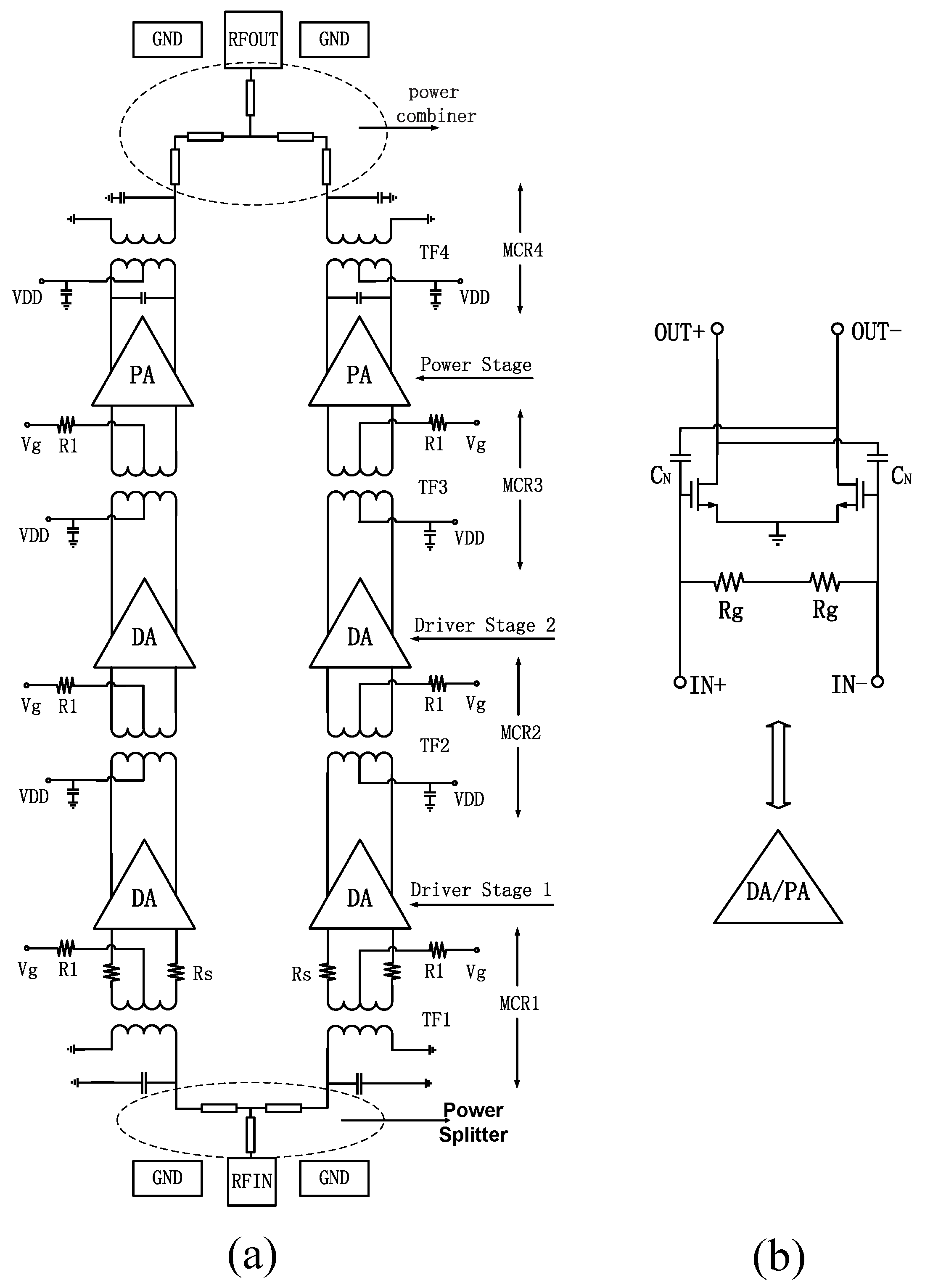
Figure 1. (a) The whole three-stage wideband power amplifier. (b) The unit stage cell of the power amplifier.
Electronics 12 03566 g001
Figure 2. The lumped model of a MCR.
Electronics 12 03566 g002
Figure 3. The lumped model of the output symmetrical MCR4.
Electronics 12 03566 g003
Figure 4. (a) The 3D view of the output transformer (TF4) in the symmetrical MCR4 and (b) its layer structure.
Electronics 12 03566 g004
Figure 5. The (a) inductance and (b) Q factor of L 1 and L 2 for the output transformer (TF4) in MCR4.
Electronics 12 03566 g005
Figure 6. (a) The coupling coefficient between L 1 and L 2 for the output transformer (TF4) in MCR4 and (b) the 3D view of the whole output matching network.
Electronics 12 03566 g006
Figure 7. (a) The insertion loss of the whole output matching network and (b) the Z21 of MCR4.
Electronics 12 03566 g007
Figure 8. The Z21 test schematic for MCR4.
Electronics 12 03566 g008
Figure 9. (a) The power gain (Gp) of power stage with the whole output matching network and (b) the input impedance of the output symmetrical MCR4 (including C 11 + C 12 of the power stage).
Electronics 12 03566 g009
Figure 10. Circuit schematic of power stage with ideal LC input matching.
Electronics 12 03566 g010
Figure 11. (a) Pout and PAE of power stage with ideal LC input-matching network at 32 GHz and (b) Pout and PAE of power stage with ideal LC input-matching network from 26 GHz to 36 GHz.
Electronics 12 03566 g011
Figure 12. Lumped model of a transformer for matching.
Electronics 12 03566 g012
Figure 13. (a) The equivalent T matching of TF3 in MCR3 and (b) the specific structure of MCR3.
Electronics 12 03566 g013
Figure 14. (a) Different TF matching trajectories from ZM1 to ZM2 on Smith Chart and (b) the chosen trajectory that both satisfies matching and ω 1 = ω 2 .
Electronics 12 03566 g014
Figure 15. The 3D view of transformer 3 (TF3) in MCR3.
Electronics 12 03566 g015
Figure 16. (a) S11 at the gate of power stage from 26 GHz to 36 GHz and (b) the Z21 of MCR3 between driver stage 2 and power stage.
Electronics 12 03566 g016
Figure 17. The lumped model of MCR2 including TF2.
Electronics 12 03566 g017
Figure 18. The Z21 of MCR2 between driver stage 1 and driver stage 2 in four different cases.
Electronics 12 03566 g018
Figure 19. (a) The 3D view of transformer2 (TF2) in MCR2 and (b) the Z21 of MCR2 between driver stage 1 and driver stage 2 with EM simulation results.
Electronics 12 03566 g019
Figure 20. (a) The lumped model of MCR1 based on TF1 for matching and (b) the 3D view of the input-matching network including TF1 and the power splitter.
Electronics 12 03566 g020
Figure 21. The Z21 of the MCR1 when the inductors and capacitors are all ideal components with a k increasing from 0.3 to 0.7.
Electronics 12 03566 g021
Figure 22. (a) The Z21 of MCR1 at the input of the power amplifier and (b) the Z21 of each MCR and the total circuit.
Electronics 12 03566 g022
Figure 23. (a) The Gmax and stability of the 128 μ m transistor used in the output differential pair versus the values of neutralization capacitance (Cneu) at 32 GHz and (b) the Gmax and Kf at different frequencies when shunt resistors are added to the output stage pair.
Electronics 12 03566 g023
Figure 24. (a) The layout of the designed wideband power amplifier and (b) the post-simulated S-parameters of the designed power amplifier.
Electronics 12 03566 g024
Figure 25. (a) The simulated S12 of the designed power amplifier and (b) Pout, PAE, and gain of the designed power amplifier at 28GHz, 31GHz, and 32GHz, respectively.
Electronics 12 03566 g025
Figure 26. (a) Pout, PAE, and gain of the designed power amplifier at 26 GHz and 36 GHz, respectively and (b) the large-signal performance of the designed power amplifier from 26 GHz to 36 GHz.
Electronics 12 03566 g026
Figure 27. (a) Post-simulated S-parameters of the designed power amplifier at ff corner and (b) the large-signal performance at ff corner from 26 GHz to 36 GHz.
Electronics 12 03566 g027
Figure 28. (a) Post-simulated S-parameters of the designed power amplifier at ss corner and (b) the large-signal performance at ss corner from 26 GHz to 36 GHz.
Electronics 12 03566 g028
Table 1. Performance comparison with the state of the art.
TCAS-II 2021 [38]TCAS-II 2021 [23]MWCL 2022 [29]ISSCC2017 [39]This Work
Technology130 nm SiGe28 nm CMOS28 nm FD-SOI40 nm CMOS65 nm CMOS
Frequency (GHz)3524/26/28/30302731/32
Peak gain (dB)25.321.21922.425.87 [email protected] GHz
3 dB S21 BW (GHz)1121.8–3026–39.826–3225.8-36.9
P s a t (dBm)22.819.7/20.3/20/2017.115.117.84/17.81
1 dB P s a t BW (GHz)7N/A12N/A10
O P 1 d B (dBm)22.618.2/18.2/17.8/17.216.113.714.09/14.04
1 dB O P 1 d B BW (GHz)N/AN/A13710
P A E m a x (%)2734.5/33.1/30/30.325.333.724.37%
VDD (V)3.32.2N/A1.11.1
Area ( mm 2 )0.480.1890.1620.2251.326
Disclaimer/Publisher’s Note: The statements, opinions and data contained in all publications are solely those of the individual author(s) and contributor(s) and not of MDPI and/or the editor(s). MDPI and/or the editor(s) disclaim responsibility for any injury to people or property resulting from any ideas, methods, instructions or products referred to in the content.