Abstract
With the specialization of VLSI ASICs for front-end signal processing electronics, the customization of the control back-end electronics (BEE) has become critical to fully deploy the ASIC performance. In the context of space operations, with typical constraints on power and reliability, the design and qualification of such integrated systems present significant challenges. In this paper, we review the design and performance of the BEE systems after two years of operations in low Earth orbit (LEO); these systems read out the custom ASICs inside the gas pixel detectors, which are located at the heart of the imaging X-ray polarimetry explorer (IXPE), a NASA-ASI small explorer mission designed to measure X-ray polarization in the 2–8 keV energy range.
1. Introduction
The imaging X-ray polarimetry explorer (IXPE) [1], launched in late 2021, is a NASA-ASI Small Explorer mission designed to perform polarization measurements in the 2–8 keV band, complemented with imaging, spectroscopy, and timing capabilities. At the heart of the focal plane is a set of three polarization-sensitive gas pixel detectors (GPDs) [2], each based on a custom ASIC acting as a charge-collecting anode, which we developed on purpose [3].
The space environment introduces a series of system constraints. Some of these are purely mechanical, relating to the solicitations during the spacecraft launch or the out-gassing properties of the materials that tend to contaminate the spacecraft with potential instrumentation damage. Heat transfer is a major concern during the design of devices operating in space due to the absence of air convection. Other constraints, more related to electronic devices, include stringent power requirements, operating temperature ranges, and radiation hardness. All of these must be managed at the system level, aiming for proper evaluation and control, and the subsystem level, via hardening techniques and device hardness effectiveness estimation. For radiation hardness, it is crucial to assess the impact of energetic particles on electronic devices in the space environment. A proper assessment relies on the analysis of energetic particle concentrations within the specific orbital context combined with device sensitivity and the secondary effects of surrounding materials.
2. Instrument Description
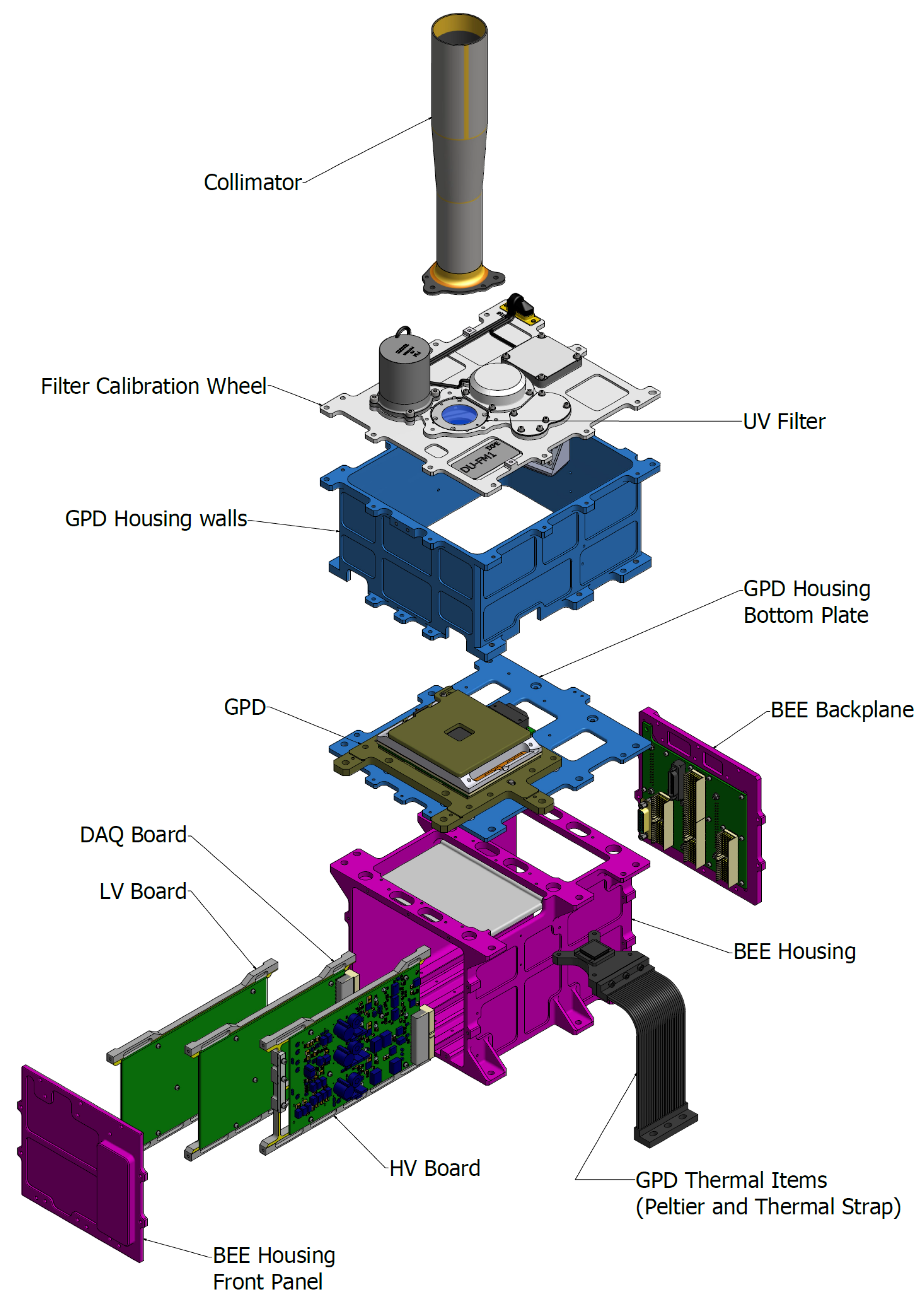
The imaging X-ray polarimetry explorer (IXPE) encompasses a set of three identical X-ray telescopes, consisting of a polarization-sensitive, imaging X-ray detector unit (DU) [4] aligned to a mirror module assembly (MMA) and separated by a deployable boom at the focal distance of 4 m, which focuses the incoming radiation from the target sources in the sky to the detectors. Each IXPE DU integrates the core imaging, polarization-sensitive gas pixel detector (GPD [2]) with its readout electronics and mechanical housing accommodating services for flight operations (see Figure 1).

Figure 1.
IXPE detector unit—exploded view; the GPD stands horizontally in the middle of the stack, just below the stray light collimator, which is in charge of preventing background radiation from entering the detector’s sensitive area. Readout electronics boards are mounted vertically at the bottom of the DU, connecting to the backplane at the rear of the DU. Custom-designed aluminum enclosures ensure robustness, offer thermal dissipation paths, and shield the entire assembly.
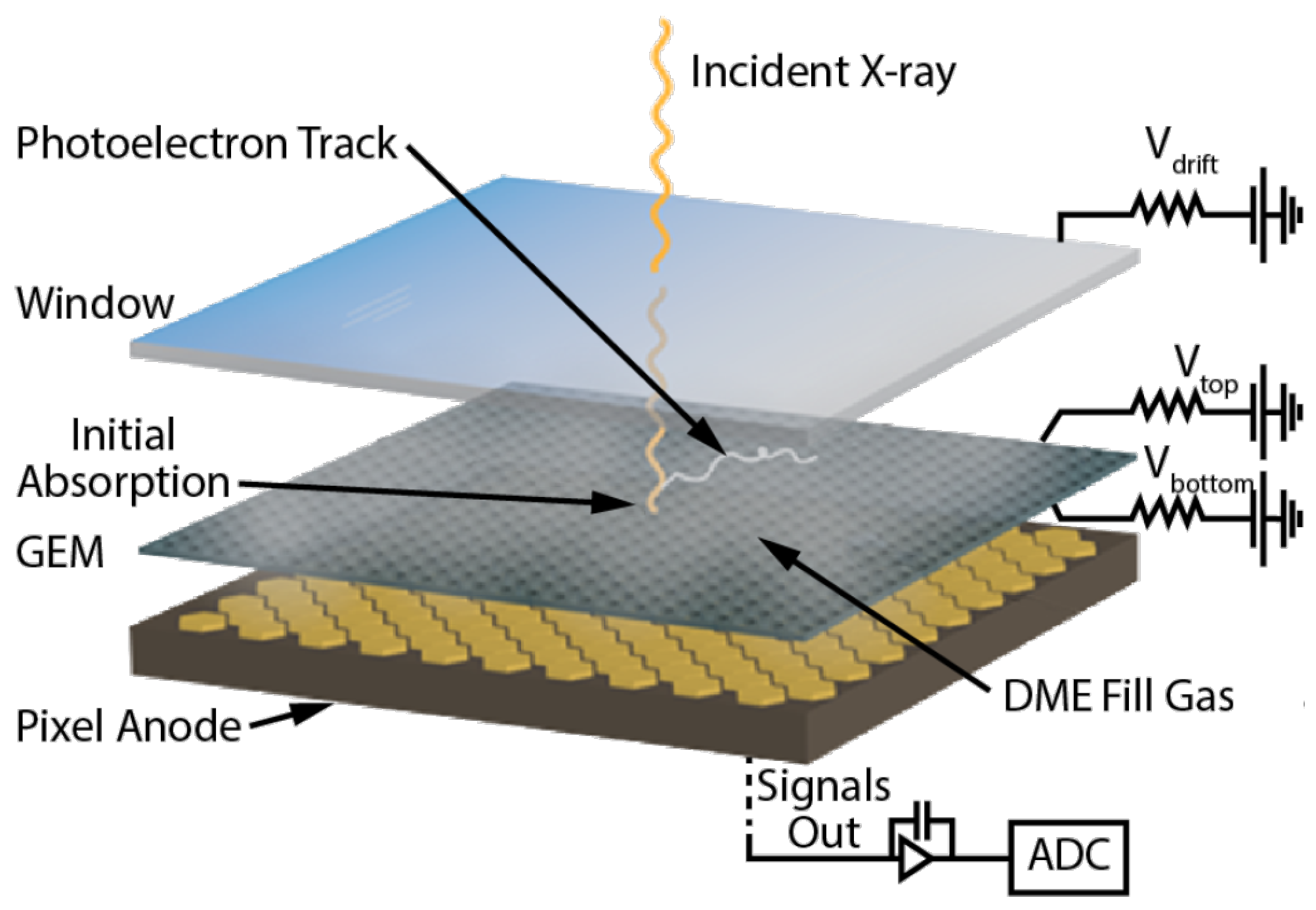
The GPD (see Figure 2) is a sealed gas pixel detector based on the same amplification principle of a proportional counter, where photons are detected and processed one by one and assigned with energy, point-of-absorption, polarization, and time-of-arrival data. The primary electrons, due to the photoelectron ionization track in pure DME gas, drift in a uniform electric field region (of the order of V/cm) toward a gas electron multiplier (GEM) stage, where, thanks to a stronger electric field (of the order of V/cm), they trigger Townsend avalanches. The result is a secondary charge distribution with the same shape but a proportionally increased number of electrons involved (at a fixed bias voltage, the GEM’s average effective gain is determined and independent of the primary charge, so that the readout electronics can easily estimate the original photon energy, being the collected charge amount that is linearly dependent on the energy of the impinging photon). This distribution can be imaged by a custom, finely pixelated (50 m pitch hexagonal pixels) application-specific integrated circuit (ASIC), namely XPOL, at the bottom of the GPD gas cell, which operates as the detector’s front-end electronics (FEE) [3,5], providing triggers, charge sensing, signal shaping, and analog event readouts to the dedicated back-end electronics (BEE). This system provides a time-of-arrival with a resolution of a few hundred ns.
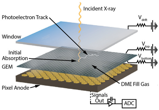
Figure 2.
GPD operational principle schematic. Photoelectric absorption occurs in the “drift region”, where a relatively weak electric field ( V/cm) makes the primary charge distribution drift toward the amplification stage (GEM). Avalanche multiplication occurs in the GEM thanks to a stronger electric field ( V/cm) in the amplification region while preserving the primary track shape. The secondary charge distribution is then transferred for readout to the pixelated ASIC readout, located at the base of the detector assembly, through a moderate electric field ( V/cm).
The photoelectron track retains information about the detected photon energy, polarization, and point-of-absorption. These are extracted by offline software that processes the ground-collected data and analyzes the photoelectron track morphology, as depicted by the XPOL readout, ASIC (see Figure 3). The single photon processing is feasible thanks to the low source intensities, which are typical for astronomical X-ray sources, and to a tailored readout architecture based on advanced capabilities that are specific to XPOL, which can finely identify a region of interest (ROI), typically made of a few hundred pixels over the entire sensitive area (>100 k pixels). The sensitivity of the polarization measurement is directly linked to the observation time, which can vary between a few days to several weeks, depending on the source intensity. Therefore, the need for a reliable and stable detector control is evident.
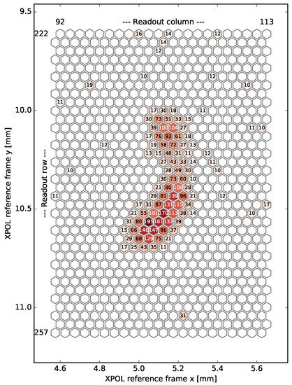
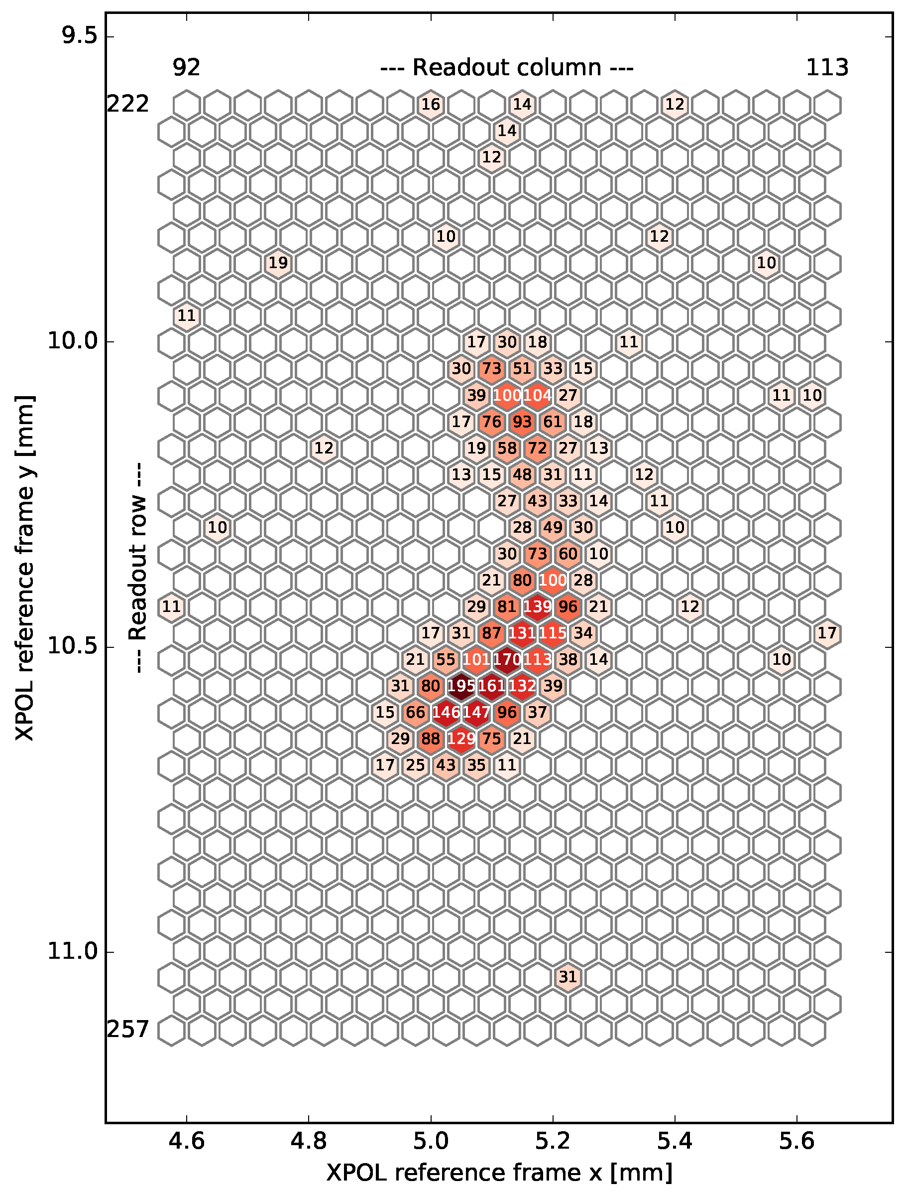
Figure 3.
Example of a real track from a 5.9 keV photon, as depicted by the GPD. Small hexagons represent pixels on the ASIC readout. X and Y real dimensions are shown for reference. Pixels with a charge content greater or equal to 10 ADC counts (corresponding to ) are displayed in color. The numbers drawn inside hexagons represent the charge detected by the pixels in ADC units (1 LSB = ). The charge distribution within the track holds the photon energy, absorption point, and polarization information. The readout electronics assign the photon’s time-of-arrival with a timing resolution of several hundred nanoseconds.
2.1. The Front-End ASIC
Years of development culminated in the creation of the 180 nm CMOS VLSI large-area chip dubbed XPOL, currently in use aboard the IXPE and PolarLight X-ray observatories [6]. XPOL is organized as a pixel matrix of 105,600 pixels on a 50 m pitch over a mm active area with a power consumption of ∼350 mW/cm. In each pixel, a charge-sensitive amplifier (CSA), shaper, peak detector, and sample and hold (S/H) circuits, are are situated below the collection anode, crafted using the top metal layer (see Figure 4a,b). The pixel’s very low noise level ( ENC) allows for efficient self-trigger functionality, which represents the core of the readout paradigm. A dedicated mixed-signal circuitry, referred to as a “mini-cluster”, is provided for every four pixels. These mini-clusters sum the charge signals of the related pixels, compare them with a global threshold that is externally applied to the ASIC by means of a voltage reference, and generate a global trigger signal whenever such a threshold is crossed. A trigger-processing logic chooses a region of interest (ROI), which encloses the triggering pixels plus a margin. The mini-cluster-based triggering scheme provides an efficient way to mitigate the effects of pixel noise and non-uniformity responses, which otherwise negatively impact the trigger efficiency. Firstly, by allocating 1 discriminator out of 4 pixels, a larger area budget becomes available, allowing for proper device-matching during the layout. Secondly, due to their stochastic nature, the dispersion in the pixel’s electrical parameters results in a factor 2 in the sum RMS, while the charge signals contribute a straight factor of 4, providing an effective increase in the trigger circuit SNR [2]. During the readout, the S/H outputs of the ROI pixels are sequentially connected at the input of an on-chip global differential amplifier, which drives the output pads. The readout sequence and signal digitization are managed by a dedicated FPGA and analog-to-digital converter (ADC) in the BEE in order to extract information about the charge collected by each pixel. The charge collection and readout processes conclude with the extraction of the data presented in Figure 3, where a typical ROI readout result is shown.
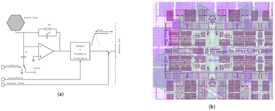
Figure 4.
XPOL in-pixel electronic symbolic representation (a). Each pixel is equipped with its own complete spectroscopic conditioning chain, made by the charge sensor amplifier (CSA), the CR-RC shaper, and a peak and hold circuitry triggered by a signal that is globally distributed to the pixel matrix. Each four-pixel group makes a mini-cluster, which provides a global trigger signal, comparing the sum of the four-pixel charge content to a global threshold that is externally applied. XPOL mini-cluster layout snapshot (b).
2.2. The Readout and Control Electronics
The IXPE’s back-end electronics (BEE) are responsible for the commanding and control of the GPD readout chip, as well as the generation of low and high voltages for the detector and the handling of the science data and telemetry interfaces. At the hardware level, the BEE consists of three distinct electronic boards plugged onto a common backplane:
- The low-voltage power supply (LVPS);
- The high-voltage power supply (HVPS);
- The data acquisition (DAQ) board.
The LVPS board generates and distributes the secondary voltages, deriving them from the main 5 V power supply by means of three independent DC/DC converters. Current sensing circuits allow for the run-time monitoring of power absorption. Finally, the high-voltage power supply board generates three high voltages needed to operate the GPD, typically 1800 V at the GPD drift electrode, defining the electric field in the drift region, 500 V across the amplification stage, and 400 V at the GEM bottom for the secondary charge collection at the FE ASIC.
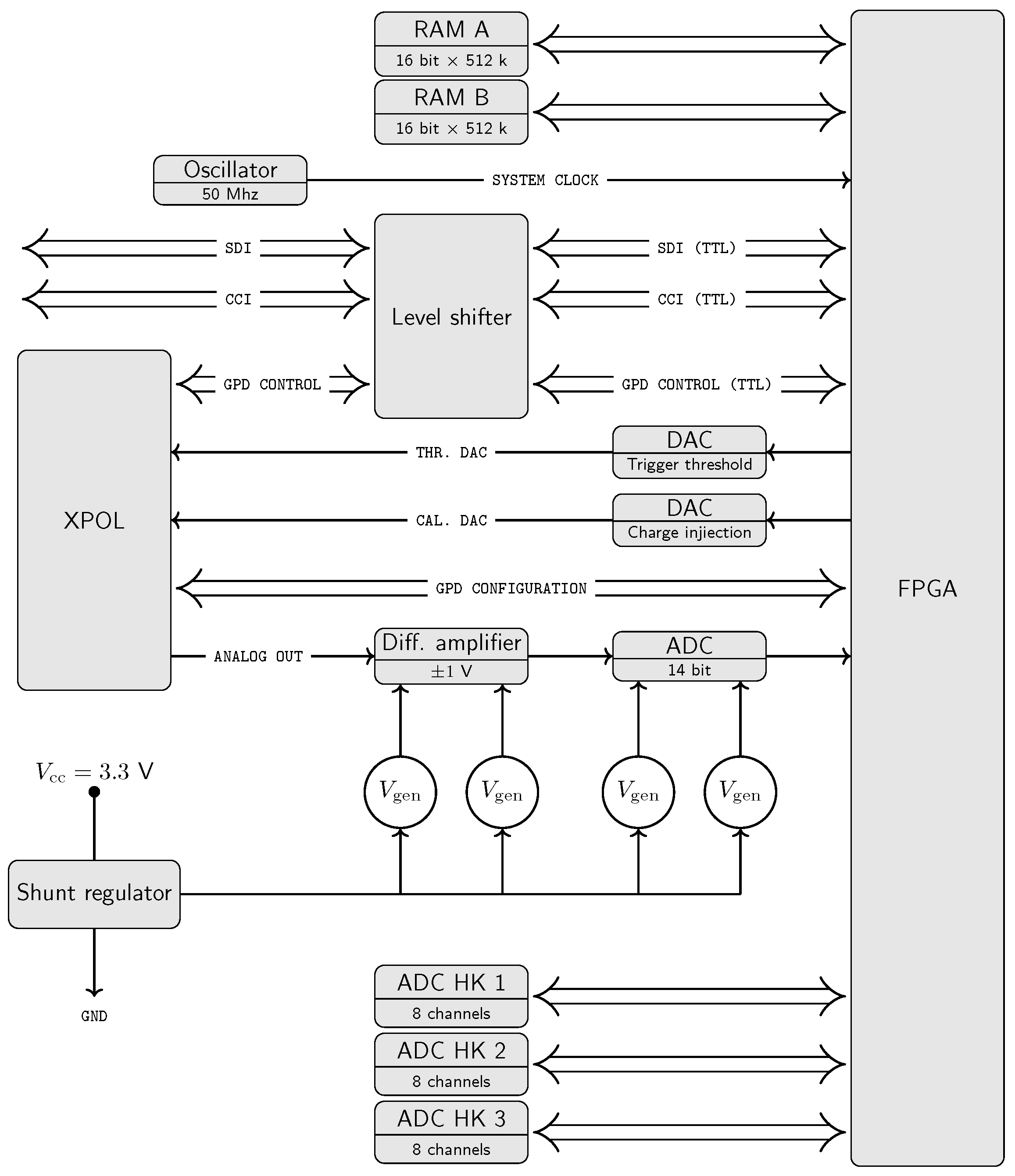
The DAQ is a mixed-signal board centered around the Microsemi RTAX2000 FPGA, which forms the core logic of the BEE, managing the GPD configuration, the control and readout, as well as the communication with the IXPE onboard computer (DSU) for the telemetry and science data transmission (see Figure 5). Sensor pixel charge information is represented by means of a differential voltage output, which is then sampled on the DAQ board by a dedicated 14-bit pipeline ADC. Two digital-to-analog converters (DAC) provide the voltage references for the proper biasing of the GPD, generating the global threshold and the calibration signal. Three multi-channel ADC sample voltages distributed throughout the whole BEE, traditionally referred to as housekeeping (HK) data, primarily monitor temperatures and currents from the secondary power supply. A set of 16 × 128 bits registers is incorporated in the FPGA logic in order to keep system configuration data and register overall BEE functional parameters. A dedicated FPGA logic manages the sampling of the HK ADCs and data storage in the designated BEE registers. The content is available for the Alarming logic (See Section 5), which is in charge of detecting and signaling anomalies in the BEE functional parameters. Additionally, the content can be acquired by the DSU through the CCI for the HK telemetry data packet composition.
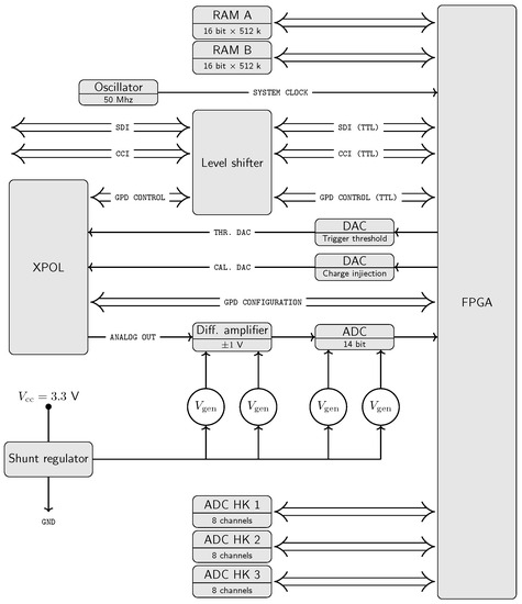
Figure 5.
DAQ board—detailed block diagram. The FPGA integrates all logic for the communication interfaces with the DSU (CCI, SDI), the GPD, the HK ADCs, the main ADC in charge of converting the GPD analog output, and the SRAMs used for data buffering. The level-shifter block encompasses the LVTTL/LVDS adapter devices.
2.3. Communication Interfaces
The BEE implements point-to-point communication with the DSU, accepting control commands and transmitting both scientific and HK data. Two independent interfaces manage the detector’s configuration, control, monitoring, and science data transmission, ensuring efficient, low-latency communications.
The command control interface (CCI) accesses the DAQ registers (to control the BEE status), while the scientific data interface (SDI) is designed for the independent transmission of detector scientific data. Both SDI and CCI make use of the low-voltage differential signaling (LVDS) standard in order to maximize electromagnetic compatibility and minimize power consumption. The CCI is based on a four-line SPI protocol with error protection mechanisms. The DSU, acting as the master device, can access the DAQ board’s internal register bank in both read and write modes, thus commanding specific DAQ functions, reading its status, and retrieving all HK quantities. Each CCI transaction represents a command issued by the DSU for the DU and implies the transmission of three 8-bit words and 1 parity bit each (27 bits in total). Parity is checked for the three words and the command is ignored if one or more errors are found. An internal counter keeps track of the number of errors and can be acquired by the DSU to verify the success of any transaction.
The SDI is reserved for the scientific event data transmission from the DU to the DSU. It is a five-line synchronous serial streaming link with hardware flow control and basic error correction mechanisms. X-ray photon data are transmitted one by one over the SDI. A CRC-16 checksum, encapsulated in variable-length SDI packets, is included in the packet body for basic error detection purposes. A deeper description of the communication interface performance can be found in [7].
3. Thermal Control
Heat dissipation is always a concern for electronic boards in space. Even with a limited power budget, the heat produced by each component must be taken away to ensure that the entire system can operate within a defined temperature range and guarantee the required performance. This is not a simple component selection problem; it has implications on the design of the entire system.
Since the electronics operate in a vacuum, there is no convection for heat transfer and conduction is only practically available for thermal control. In general, passive systems are preferred to maximize reliability. The boards are in good thermal contact with the housing, which in turn is in contact with the spacecraft structures acting as heat sinks. The BEE is not an exception. While the backplane is completely in contact with the housing, the three boards are mounted vertically on an aluminum frame that has been specifically designed to provide mechanical support and to transfer the heat toward the bottom of the BEE housing. In this way, the GPD is shielded from the heat generated by the BEE, allowing for more efficient thermal control. More specifically, there is only one rail for each board at the bottom of the housing that keeps the boards in place, maximizing the heat transfer on this side. The entire DU is placed on an adapter plate whose temperature is actively controlled by the spacecraft. The plate is directly connected to a radiator by means of a thermal strap for cooling, and resistive heaters are installed as well. Each board is monitored with two temperature sensors (three for the LVPS), placed in critical areas, to monitor the system’s behavior in orbit and during tests. Table 1 lists a simplified power budget breakdown for the IXPE readout electronics.

Table 1.
IXPE readout electronics nominal power consumption.
The initial design of the BEE included wide margins on the temperature range (both for operation and in survival mode), e.g., by selecting MIL-standard components. Subsequent thermal analyses and vacuum tests identified the operational BEE thermal requirement to be in the temperature range between 0 and +50 °C. Finally, operations in orbit showed that the actual range can be further reduced without exceeding the allocated power budget. The actual set points depend on satellite orientation, but stability during a single scientific observation remains under 1 °C.
The detector thermal control is more complex since it has different requirements than the electronics. It uses an active thermal control system based on three heaters, one thermoelectric cooler (TEC), and a dedicated thermal path to the adapter plate. The details of the GPD’s thermal control system are beyond the scope of this paper.
4. Radiation Effects
The energetically charged particles present in space can impact the functionality of the detector electronics. Some of the effects that this radiation can cause include electrical transients, digital circuit soft errors, permanent device performance deterioration, and even the destruction of the device itself. The three main components of radiation are galactic cosmic rays (GCRs), solar energetic particles (SEPs), and trapped particles [8].
GCRs mainly consist of protons and heavy ions and originate from outside of the solar system. Even though ions from hydrogen to uranium can be found in GCRs, ions from hydrogen to iron represent the vast majority. SEPs are transient events associated with solar activity, particularly solar flares and coronal mass ejections (CMEs). They are composed of electrons, protons, and heavy ions. Proton peak fluxes as high as 10 scmsrMeV can be registered at 1 AU [9]. Even though they are quite rare, high-intensity SEP events can significantly affect space instrumentation behavior.
The trapped particle population primarily consists of electrons, protons, and heavy ions, and is the result of GCRs and SEPs interacting with the magnetosphere. These particles form the Van Allen belts that extend from 0.2 to 2 Earth radii (1000–12,000 km) and from 3 to 10 Earth radii (13,000–60,000 km). Due to the asymmetry in the Earth’s magnetic field, the inner belt reaches altitudes as low as 200 km in a region known as the South Atlantic Anomaly (SAA). In addition, the inner belts bend at the poles, where charged particles can be found in much higher concentrations at relatively low altitudes.
In a more specific context, like that of a spacecraft orbiting the earth at low altitudes, the exposure to these energetic particles depends on local factors, like interactions with magnetic fields, solar wind, and atmosphere filtering effects. Solar wind has a sweeping effect on particles; thus, a higher GCR flux is detected during a minimum of solar activity, and vice versa. Also, trapped proton fluxes are found to be higher when a solar activity minimum is detected; this is due to the effects of the solar flux on the upper atmosphere [10]. It must be pointed out that particle fluxes must be accounted for, together with their energy distribution, since energy deposition in the devices, shielding effectiveness, and secondary particle fluxes strictly depend on the primary particle energy. Indeed, low-energy particles pose a greater concern for designers as they release much more energy than their high-energy counterparts. Radiation exposure definitely depends on the spacecraft’s orbit parameters (Perigee, Apogee, inclination), as well as on the solar activity during the flight. During the mission radiation plan assessment, engineers are typically interested in determining the SEE rates and the TD in the mission’s lifetime, referring to the “worst case” condition. There are several tools available for the radiation environment; effect determination, data, and plots in this paper were generated in SPENVIS [11], the ESA’s SPace ENVironment Information System, which provides a reliable interface of models for estimations of the space environment radiation and its effects on electronics. The IXPE spacecraft orbits at a 600 km altitude with a 0.2° inclination. In terms of radiation exposure, such equatorial orbits are rather steady, and considerably high trapped particle fluxes are only expected in a small portion of the route, corresponding to the lower part of the SAA.
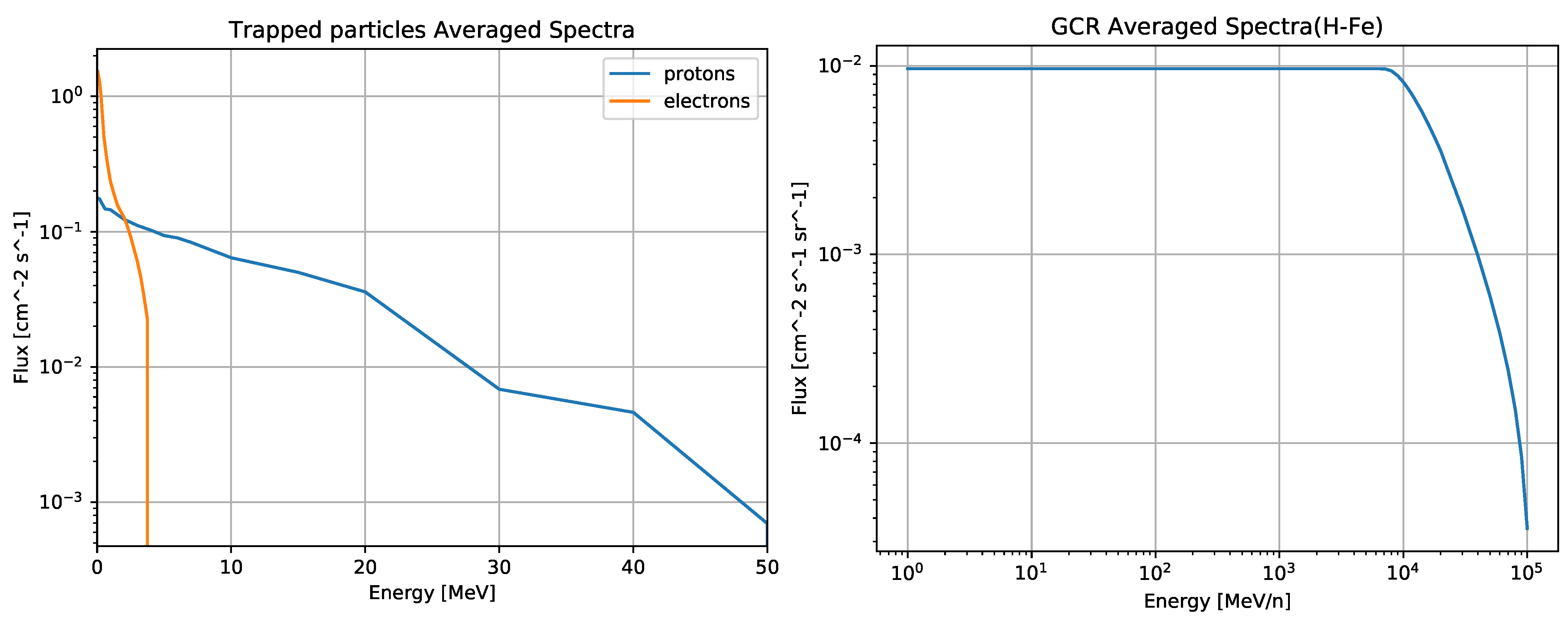
Figure 6 shows trapped particles and worst-case averaged fluxes of GCR for the IXPE spacecraft. As per the AE-8 and AP-8 model estimations, low-energy electrons can be registered with fluxes on the order of a few per second per cm, while less frequent, more energetic protons are expected at rates on the order of one within tens of seconds. Nuclei fluxes due to the GCR are expected with rates of one per minute. It should be noted that such fluxes are calculated at the spacecraft’s external shell. Filtering effects and secondary radiation due to shielding materials also play a role in the radiation exposure of electronic components. In particular, low-energy trapped particle fluxes are reduced by two orders of magnitude by a single 0.5 g/cm (ca 1.85 mm) aluminum shield. Total ionizing dose and single-event effects rates are calculated by integrating spectra over the proper energy range, combined with shielding effectiveness and device sensitivity. Such processing is typically performed using advanced tools, like Geant4 [12], simulating complex interactions between energetic particles and matter. With respect to the IXPE mission, the estimated total ionizing dose for DU electronics devices is as low as a few rad, and its effect can be neglected. In terms of SEE rates estimation, trapped particles and GCR fluxes must be convoluted with device-specific SEE cross-sections.
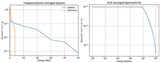
Figure 6.
Trapped protons and electrons (left) and GCR nuclei (right) fluxes averaged on the LEO 0.2° inclination orbit. Data from AP-8, AE-8, and CREME-96 models with solar activity, at minimum.
Radiation Sensitivity in Readout Electronics
When talking about radiation effects, a distinction between single-event effects (SEEs) and total dose (TD) effects must be conducted. While the previous are measured by their probability of occurrence, which results as a combination of the particle fluxes and the device-specific sensitivity (i.e., SEE cross-section), the TD effect estimation focuses more on the evaluation of the device performance dependence on the total dose deposited to the device. A detailed description of the processes related to the ionizing and non-ionizing radiation exposure is beyond the scope of this paper, which focuses on the overall flow adopted for the BEE device verification. Due to the very low TD foreseen in the IXPE mission, we concentrated on the evaluation of expected SEE rates, specifically the single-event latch-up (SEL) and single-event upset (SEU) rates, according to the radiation hardness assurance program specified in [13]; this program is a standard from the European Cooperation for Space Standardization (ECSS). All the BEE components were found to be free of any potentially destructive failures, like latch-up and gate rupture or burnout. For most of the electronic devices in the BEE, we relied on the manufacturer radiation assessment reports required for typical space qualifications; for the GPD, we performed irradiation tests ourselves. As the GPD is a complex system, radiation hardness was analyzed in two separate steps: one aimed to verify the overall GPD with interest in the amplification stage in the gas detector, and the other aimed to assess the ASIC readout radiation hardness. Several heavy ion accelerator facilities are available worldwide, differentiating between the beam specifications. We performed irradiation tests on the XPOL ASIC at the SIRAD facility at the INFN National Laboratory of Legnaro in Padova. We analyzed performance during exposure to high-energy nuclei at different LETs, extrapolating SEE cross-sections and TD effects. No SEE, other than regular and expected SEU sensitivity or performance degradation, was spotted after irradiating with several ion species (F, Cl, Br, I) for an overall TD greater than 500 krad. Table 2 lists a summary of the main devices’ SEU rates and estimated worst-case failure rates. The overall GPD hardness verification tests were performed at the Heavy Ions Medical Accelerator in Chiba (HIMAC, Ibaraki, Japan), with no significant damage after total exposure to more than Fe ions, corresponding to more than 40 years in space in low Earth orbit.
Table 2.
IXPE BEE’s main EE parts, SEU cross-sections, and worst-case mean time between failures.
Even though no issues were spotted in the radiation assessment plan, we introduce some hardening features to establish the ultimate level of system reliability (see Section 5).
5. Hardening
At the system level, ’Hardening’ refers to design practices that have been accomplished at the device level and software level. Generally speaking, the IXPE BEE hardening for the space environment meant putting together a set of design choices that affected the device selection, electrical scheme drawing, FPGA logic, communication protocol, and data format specification. In the following sections, we describe some general hardening techniques that have been adopted by manufacturers when designing the devices selected for the BEE, as well as more specific features developed by the IXPE BEE designer team.
5.1. Device Selection
FPGAs are the primary choice when assembling complex sequential logic. Sequential logic suffers from SEU sensitivity at the state memory registers. Those SEUs can infer random behaviors in counters or finite state machines (FSMs). Such issues are usually treated using majority voter logic schemes at the expense of a greater area budget and performance degradation. The configuration memory itself can experience SEU. The device that we selected tackles the configuration issue by means of a highly reliable anti-fuse one-time programming technology. While being the most reliable solution to the problem, one-time-programmable (OTP) FPGAs add a bit of complexity to the firmware development phase. High-reliability FW design techniques as well as accurate post-fitting timing analyses granted us a peaceful path to the flight FW release, which happened to be exactly the same as the very first OTP device that we programmed for the BEE engineering model (EM). SEU sensitivity in the user logic registers is managed by a compact majority voting scheme implemented in hard silicon, transparent to the designer, which can describe the user logic and avoid the complexity of the voting logic implementation in the HDL design.
5.2. BEE Alarming
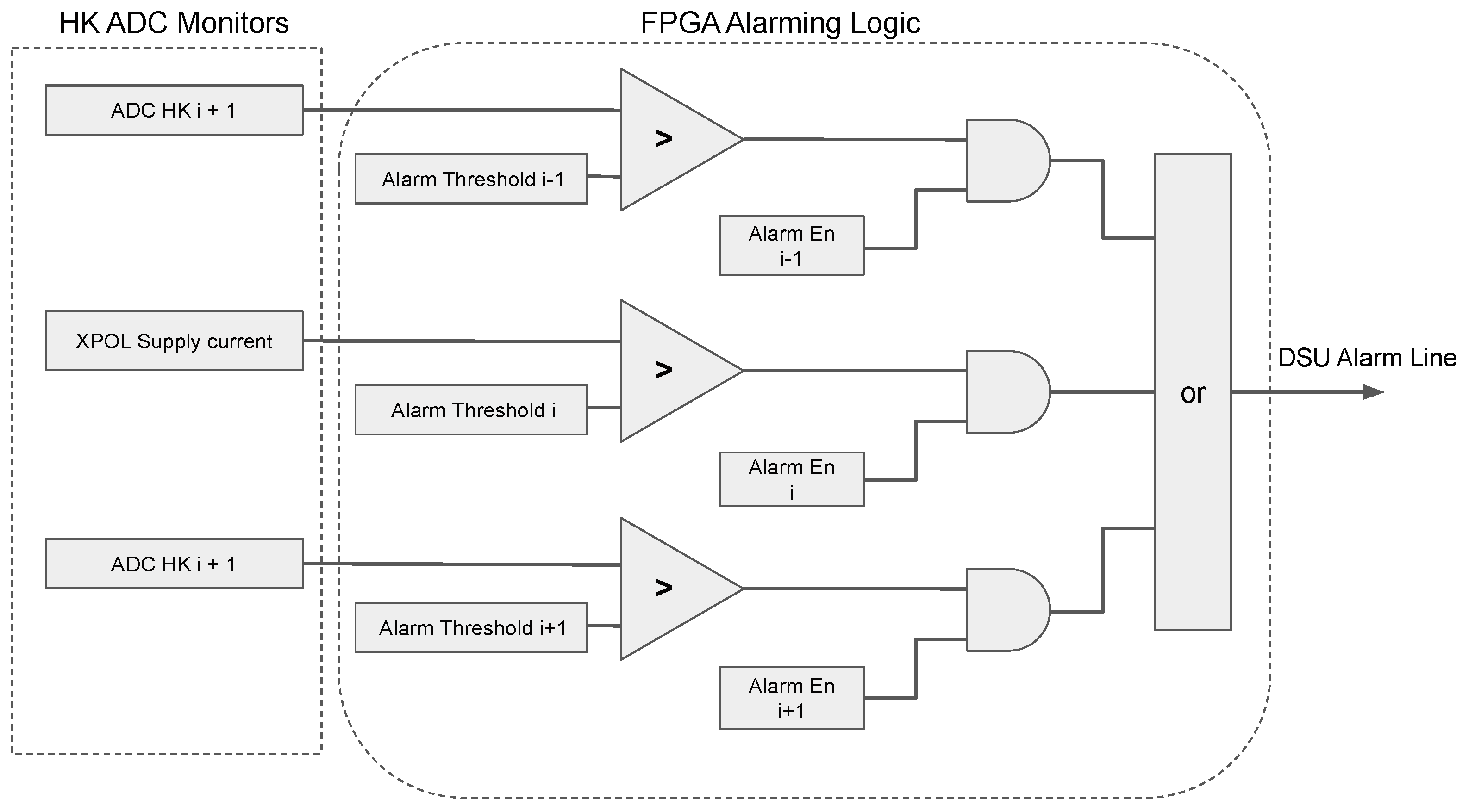
Even though each EE component had to be tested and qualified for SEE sensitivity, the final results are inevitably affected by uncertainties and, when it comes to potentially destructive events like latch-ups, a way-out strategy shall be considered anyway. Typical approaches to the latch-up mitigation make use of resettable fuses or implement feedback circuits, monitoring the current delivered to a specific sub-circuit and interrupting the power supply line when an anomalous current rise is detected. Implementing such strategies at the circuit level guarantees the shortest intervention times, but it requires careful design. Failure rates of the additional circuitry could be higher than the SEL rate itself. In the IXPE BEE, there is an additional criticality related to the high-voltage detector bias, which requires proper ramping-up and ramping-down procedures to be synchronized with the BEE power supply control. If not, it can be fatal to the detector itself. In the IXPE BEE, we took advantage of the FPGA flexibility to implement a configurable alarm system, which is symbolically depicted in Figure 7. Data from multi-channel ADCs (HK1, HK2, HK3 in Figure 5) devoted to the HK sampling are checked on the FPGA itself and compared to thresholds programmed in the register bank. If an over-threshold condition occurs, then an alarm condition is signaled to the DSU via a dedicated line. A fault detection, isolation, and recovery routine (FDIR), executed on the DSU, checks the alarm code by accessing the register bank only once, and applies the proper recovery strategy that, in case of an unexpected increase of a power supply current, consists of a DU power cycle. Such a highly ”at run-time” configurable alarming scheme is a reasonable trade-off between short intervention times and detector safety.
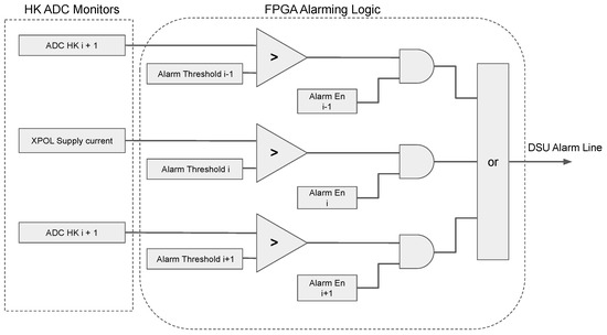
Figure 7.
Symbolic representation of the alarming logic implemented in the IXPE DU FPGA. Functional parameters (HK), like boards, temperature, and secondary power supply output currents are monitored and verified against a programmable digital threshold. If an over-threshold condition occurs, a dedicated line to the DSU signals the alarm condition. Channels can be individually enabled/disabled by a designated configuration register bit.
5.3. Error Detection
Access to the BEE register bank through the CCI is reinforced by a parity bit error detection mechanism. Parity bits are effective at detecting single-bit errors, where only one bit in the transmitted data is flipped or corrupted during transmission. Since the DSU transmits configuration commands to the DU through the CCI, a transmission error could infer anomalies in the system behavior. In such cases, the BEE FPGA’s parity check logic will identify the error, reject the command, and augment a dedicated error counter. Transmission errors can be detected on both sides, allowing for a proper recovery procedure execution.
In the SDI, the error detection mechanism is based on the CRC-16 checksum calculation and verified on the SDI packet payload. The DSU verifies the packet’s CRC-16 with a locally calculated CRC to detect data corruption. The DSU can request packet retransmission for a limited number of times. If errors persist, the packet is flagged with an error code in the designated header location but is still transmitted to the ground station. It is important to note that communication interface errors can be caused by transmission errors or single-event upsets (SEUs) occurring in the BEE memory. In the latter case, checksum checks would fail on the retransmitted packets as well.
6. In-Orbit Operations
During in-orbit operations, we continuously check the functionality of the detector units by means of several monitors; some are analog, measuring temperatures and power supply output currents, and others are digital, monitoring the data transmission statistics.
Digital counters in the DSU keep track of the total number of errors detected at the CCI (parity errors) and SDI (CRC errors) interfaces. These counters are periodically sent to the ground station via telemetry as part of the standard HK information. Table 3 summarizes the error statistics observed in orbit.
Table 3.
IXPE BEE in-orbit error statistics.
At the time of this writing, we collected about 520 days of fully functional operations without any issue in the BEEs for an operation time of about ∼ s (the acquisition was paused during SAA passage, for about 11% of the total time). We did not experience any interruption due to an alarm or other issues with our electronics. Moreover, we did not record any errors in the CCI, indicating the absence of any errors in the FPGA register bank.
We acquired data at an average rate of about 4.5 events per second in each DU, including both scientific observations and calibration sources. We registered only three CRC errors in the SDI at DU1. These three events were sent to the ground after subsequent successful retransmission.
Four radioactive sources, namely CalA, CalB, CalC, and CalD, are directed toward the GPD to periodically verify the X-ray detector’s overall performance and derive calibration parameters. Figure 8 shows a charge map resulting from the superposition of a recent in-orbit observation of the Fe-55 CalC calibration source onto the DU1 sensor. In the map, each pixel corresponds to a physical pixel in the detector and its content represents the total integrated charge (in ADC counts) during the observation. Figure 9 shows the pulse height distribution for the same observation. The distribution, fitted with a Gaussian model, peaks at 18,500 ADC counts, corresponding to the characteristic 5.9 keV energy photons emitted by the Fe-55 source. For the purpose of this paper, the peak position and dispersion (Sigma, Kawasaki, Japan) are the main figures of merit, indicating the entire system’s integrity. In-orbit calibration data are perfectly aligned with the pre-flight data, meaning that both the GPD and the readout electronics have been consistently operating with no significant deviation since the IXPE’s launch in late 2021.
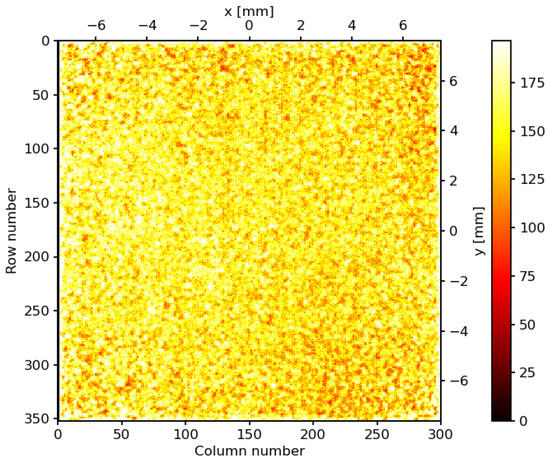
Figure 8.
DU1 sensor charge map. Each pixel on the map represents a detector’s physical pixel. The intensity scale, expressed in ADC units (1 LSB = ), is proportional to the total charge integrated during the CalC calibration source (Fe-55). Photons are processed one by one, and the charge map is developed by multiple-track superposition.
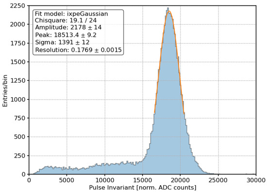
Figure 9.
CalC (FE-55) spectrum in ADC units (1 LSB = ), collected at the DU1 sensor. Each photon is processed individually for energy, position, and time tagging. The Energy of the detected photon is calculated, starting from the overall charge content in the pixels belonging to the track in the ROI. This charge is then histogrammed. A Gaussian model (orange line) fits the distribution at the main peak. The peak position corresponds to the 5.9 keV characteristic of the Fe-55 radioactive source. The tail on the left of the photo peak is expected and is due to photoelectrons losing some of their energy in the non-active areas of the detector.
7. Conclusions
Space instrumentation is expected to face strong mechanical solicitation during rocket launches and extended temperature ranges. Moreover, space can be a hostile environment for electronic equipment due to the presence of energetic radiation, which could potentially induce malfunctions and even result in device destruction. We provided a design overview, addressing major concerns in complex space electronics systems, with reference to detector units, which we developed for the IXPE X-ray observatory. After almost two years of operation in an equatorial LEO orbit, our experimental results demonstrate the success of our quite demanding engineering efforts. The initial IXPE lifetime expectation was three years, with at least two functioning DUs out of the total three. After almost two years of operation, the entire instrument is fully functional, with no significant deviations from its pre-launch performance.
Author Contributions
Conceptualization, M.M. (Massimo Minuti) and C.S.; methodology, M.M. (Massimo Minuti) and C.S.; software, M.M. (Massimo Minuti), C.S., L.B. and A.M. (Alberto Manfreda); resources, all authors; writing, M.M., C.S., L.B., L.L. (Luca Latronico), L.L. (Leonardo Lucchesi), L.O. and M.P.-R. All authors have read and agreed to the published version of the manuscript.
Funding
This research was funded by the Italian Space Agency (ASI), grant numbers ASI-OHBI-2017-12-I.0, ASI-INAF-2017-12-H0, ASI-INFN-2017.13-H0, the ASI Space Science Data Center (SSDC), the italian Istituto Nazionale di Astrofisica (INAF), the italian Istituto Nazionale di Fisica Nucleare (INFN).
Data Availability Statement
IXPE scientific data are available at https://heasarc.gsfc.nasa.gov/docs/heasarc/missions/ixpe.html. Engineering data are private.
Conflicts of Interest
The authors declare no conflict of interest. The funders had no role in the design of the study; in the collection, analyses, or interpretation of data; in the writing of the manuscript; or in the decision to publish the results.
Abbreviations
The following abbreviations are used in this manuscript:
| ADC | analog-to-digital converter |
| ASIC | application-specific integrated circuit |
| BEE | back-end electronics |
| CSA | charge sensor amplifier |
| DAC | digital-to-analog converter |
| DU | detector unit |
| DSU | detector service unit |
| EE | electrical and electronics |
| ENC | equivalent noise charge |
| ECSS | European Cooperation for Space Standardization |
| FPGA | field programmable gate array |
| FSM | finite state machine |
| FW | firmware |
| GCR | galactic cosmic ray |
| GEM | gas electron multiplier |
| GPD | gas pixel detector |
| HDL | hardware description language |
| HK | housekeeping |
| HV | high voltage |
| HVPS | high-voltage power supply |
| IC | integrated circuit |
| LEO | low Earth orbit |
| LET | linear energy transfer |
| LVPS | low-voltage power supply |
| MTBF | mean time between failures |
| OTP | one-time programmable |
| ROI | region of interest |
| RMS | root mean square |
| SAA | South Atlantic Anomaly |
| SEE | single-event effect |
| SEL | single-event latch-up |
| SEU | single-event upset |
| SEFI | single-event functional interruption |
| SEP | solar energetic particle |
| SRAM | static random access memory |
| S/H | sample and hold |
| TD | total dose |
| TEC | thermoelectric cooler |
| VLSI | very large-scale integration |
References
- Weisskopf, M.C.; Soffitta, P.; Baldini, L.; Ramsey, B.D.; O’Dell, S.L.; Romani, R.W.; Matt, G.; Deininger, W.D.; Baumgartner, W.H.; Bellazzini, R.; et al. Imaging X-ray Polarimetry Explorer: Prelaunch. J. Astron. Telesc. Instrum. Syst. 2022, 8, 026002. [Google Scholar] [CrossRef]
- Baldini, L.; Barbanera, M.; Bellazzini, R.; Bonino, R.; Borotto, F.; Brez, A.; Caporale, C.; Cardelli, C.; Castellano, S.; Ceccanti, M.; et al. Design, Construction, and Test of the Gas Pixel Detectors for the IXPE Mission. Nucl. Instrum. Methods Phys. Res. Sect. A Accel. Spectrometers Detect. Assoc. Equip. 2021, 103, 552–562. [Google Scholar] [CrossRef]
- Bellazzini, R.; Angelini, F.; Baldini, L.; Bitti, F.; Brez, A.; Ceccanti, M.; Latronico, L.; Massai, M.; Minuti, M.; Omodei, N.; et al. Reading a GEM with a VLSI pixel ASIC used as a direct charge collecting anode. Nucl. Instrum. Methods Phys. Res. Sect. A Accel. Spectrometers Detect. Assoc. Equip. 2004, 535, 477–484. [Google Scholar] [CrossRef]
- Soffitta, P.; Baldini, L.; Bellazzini, R.; Costa, E.; Latronico, L.; Muleri, F.; Monte, E.D.; Fabiani, S.; Minuti, M.; Pinchera, M.; et al. The Instrument of the Imaging X-ray Polarimetry Explorer. Astron. J. 2021, 162, 18. [Google Scholar] [CrossRef]
- Bellazzini, R.; Spandre, G.; Minuti, M.; Baldini, L.; Brez, A.; Cavalca, F.; Latronico, L.; Omodei, N.; Massai, M.; Sgrò, C.; et al. Direct reading of charge multipliers with a self-triggering CMOS analog chip with 105k pixels at 50 μm pitch. Nucl. Instrum. Methods Phys. Res. Sect. A Accel. Spectrometers Detect. Assoc. Equip. 2006, 566, 552–562. [Google Scholar] [CrossRef]
- Feng, H.; Jiang, W.; Minuti, M.; Wu, Q.; Jung, A.; Yang, D.; Citraro, S.; Nasimi, H.; Yu, J.; Jin, G.; et al. PolarLight: A CubeSat X-ray Polarimeter based on the Gas Pixel Detector. Exp. Astron. 2019, 47, 225–243. [Google Scholar] [CrossRef]
- Barbanera, M.; Citraro, S.; Magazzú, C.; Manfreda, A.; Minuti, M.; Nasimi, H.; Sgró, C. Initial Tests and Characterization of the Readout Electronics for the IXPE Mission. IEEE Trans. Nucl. Sci. 2021, 68, 1144–1151. [Google Scholar] [CrossRef]
- Badhwar, G.D. The Radiation Environment in Low-Earth Orbit. Radiat. Res. 1997, 148, S3–S10. [Google Scholar] [CrossRef]
- Biji, M.S.; Prince, P.R. A study of the characteristic properties of SEP events observed by SOHO ERNE during solar cycle 24. Adv. Space Res. 2022, 69, 2902–2920. [Google Scholar] [CrossRef]
- Huston, S.L.; Kuck, G.A.; Pfitzer, K.A. Solar cycle variation of the low-altitude trapped proton flux. Adv. Space Res. 1998, 21, 1625–1634. [Google Scholar] [CrossRef] [PubMed]
- Heynderickx, D.; Quaghebeur, B.; Wera, J.; Daly, E.J.; Evans, H.D.R. New radiation environment and effects models in the European Space Agency’s Space Environment Information System (SPENVIS). Space Weather 2004, 2, S10S03. [Google Scholar] [CrossRef]
- Agostinelli, S.; Allison, J.; Amako, K.; Apostolakis, J.; Araujo, H.; Arce, P.; Asai, M.; Axen, D.; Banerjee, S.; Barrand, G.; et al. Geant4—A simulation toolkit. Nucl. Instrum. Methods Phys. Res. Sect. A Accel. Spectrometers Detect. Assoc. Equip. 2003, 506, 250–303. [Google Scholar] [CrossRef]
- ECSS-Q-ST-60-15C; Radiation Hardness Assurance—EEE Components. European Cooperation and Space Standardization (ECSS): Noordwijk, The Netherlands, 2012.


Disclaimer/Publisher’s Note: The statements, opinions and data contained in all publications are solely those of the individual author(s) and contributor(s) and not of MDPI and/or the editor(s). MDPI and/or the editor(s) disclaim responsibility for any injury to people or property resulting from any ideas, methods, instructions or products referred to in the content. |
© 2023 by the authors. Licensee MDPI, Basel, Switzerland. This article is an open access article distributed under the terms and conditions of the Creative Commons Attribution (CC BY) license (https://creativecommons.org/licenses/by/4.0/).