Article

A Switchable Frequency Selective Rasorber with a Broad Transmission Window at the X-Band

School of Microelectronics, Shandong University, Jinan 250100, China
*
Author to whom correspondence should be addressed.
Electronics 2023, 12(18), 3941; https://doi.org/10.3390/electronics12183941
Submission received: 14 August 2023 / Revised: 9 September 2023 / Accepted: 11 September 2023 / Published: 19 September 2023
(This article belongs to the Section Circuit and Signal Processing)

Abstract

:
This paper proposes a switchable polarization-insensitive frequency selective rasorber (FSR) within the X-band. The FSR comprises a lossy layer, a lossless layer, and an intermediate air layer. The lossy layer consists of metal patches, folded wires, and lumped resistors, while the lossless layer is formed with square and cross patches loaded with PIN diodes. An equivalent circuit model (ECM) has been developed to analyze and verify the working principle of the system. By altering the state of the PIN diodes, it is feasible to switch between absorbing and transmitting modes. In the rasorber mode, the switchable FSR attains a transmission window ranging from 10.13 to 12.27 G H z with a minimum insertion loss below 2 d B and a broad absorption band covering 5.79–15.37 G H z . When switched to absorber mode, the passband is negated, and the FSR exhibits a low transmission band from 10.68 to 18.00 G H z . This innovation can improve the omni-directional stealth capability and battlefield survivability of radar systems, possessing substantial research importance and practical applications.

1. Introduction

The frequency selective rasorber (FSR) is a multi-layer composite structure that typically consists of a lossless layer and a lossy layer cascaded together [1,2,3,4,5,6,7,8]. Utilizing the absorbing and transmitting electromagnetic characteristics of the FSR, the technology does not hinder the standard communication of the antenna, enabling out-of-band stealth, and is thereby widely employed in antenna stealth designs [9,10,11,12,13]. Within the absorbing band, the FSR exhibits all-reflective characteristics. While in the transmissive band, the bandpass frequency selective surface (FSS) [14,15,16,17] provides transmission functionality, allowing the incident wave to pass through with minimal loss. Historical designs of integrated absorbing and transmitting structures can be traced back to a 1995 patent [2], in which W.S. Arceneaux crafted a transmission absorber mask by merging a lossless bandpass FSS with a lossy absorbing dielectric plate. This structure included three layers: an artificial loss layer, a dielectric layer, and a bandpass frequency selective surface layer. The transmission rasorber combined the wave-transparent property of the FSS with the wave-absorbing property of metamaterials, setting the groundwork for subsequent FSR structures. In 2012, F. Costa [18,19] from the University of Pisa further enhanced this concept, devising a low-frequency wave-transparent/high-frequency wave-absorbing FSR using a low-frequency bandpass FSS. This design achieved integrated wave-absorbing and wave-transparent properties, and an equivalent circuit model (ECM) analysis method was also introduced. The evolution of the FSR continued in 2013 when Liu et al. [20] proposed a design featuring low-frequency wave transparency and high-frequency wave absorption. This design employed two differently sized lossy square loops to extend the absorption bandwidth and modified the bandpass layer with a bent slit cross to reduce the cell size. Subsequent contributions in 2014 by Shang et al. [21] combined square-ring arrays and cross-dipole arrays to create an FSR that absorbed waves on both sides of the transmission band. By introducing lumped resistors into metal cells of varying sizes, double resonance absorption was achieved, resulting in high- and low-frequency absorption bands. Huang et al. [22] introduced an absorptive-transmissive FSR in 2017, employing a square-ring hybrid resonator and a bent bandpass layer based on slit crosses to extend the absorption bandwidth. This design yielded a low insertion loss of 0.29 d B at 6.10 G H z and an S 11 parameter of less than −10 d B in the 2.80–9.80 G H z frequency range. In 2019, Guo et al. [23] proposed a dual-passband FSR with impedance poles realized through a double resonance structure in the center of the impedance layer. The depletion-free layer incorporated a double passband FSS with two slit structures, achieving transmission windows at 7.20 G H z and 13.05 G H z . These advancements have contributed valuable insights to the theoretical and practical design of FSRs, and most of the recent proposals continue to be grounded in this foundational structure.
The conventional passive FSR possesses a fixed structure, resulting in unchangeable filter characteristics. When the surrounding electromagnetic environment changes, the single filter characteristic of the passive FSR fails to adapt to evolving requirements. With the rapid development and wide application of wireless communications and microwave technology, the future electromagnetic environment is bound to become more and more complex. In order to make more efficient use of limited electromagnetic resources, electromagnetic control technology will also usher in a more prosperous development. To overcome this limitation, the active frequency selective rasorber (AFSR) has been introduced, enabling the achievement of different electromagnetic properties within the same FSR through human intervention. According to the cell structure of FSRs, FSRs can be categorized into 3D FSRs [24,25,26,27,28,29] and 2D FSRs [30,31,32,33,34,35,36,37,38,39]. Moreover, 3D FSRs generally contain at least two types of resonant structures, depleted and less depleted structures, which produce absorbing and transmissive resonant modes, respectively. In the 3D designs, these two resonant modes are almost independent of each other to ensure that the wave-absorbing and wave-transmitting properties do not affect each other as much as possible. And the 3D FSR design theory is based on the fundamental transmission mode of the parallel-plate waveguide structure, constructing a resonant cavity and making the resonant cavity exhibit different characteristics by loading metal strips with collector elements [24,25]. The loss characteristics are realized by placing metal strips loaded with lumped resistors [26,27], ferrite absorbers [28], and magnetic absorbers inside the cavity [29]. In 2016, Yu et al. [26] proposed a 3D absorptive-permeable unitary structure consisting of open and shorted parallel-plate waveguides. The passband was obtained by lossless open parallel-plate waveguides, and the two absorption bands located on both sides of the passband were generated by lossy shorted parallel-plate waveguides loaded with sheet resistors. The two absorption bands on either side of the passband were generated by lossy short-circuit parallel-plate waveguides loaded with sheet resistors. A capacitor was inserted into the shorted parallel-plate waveguide to form an additional resonant cavity, which greatly extends the bandwidth of the high-frequency absorption band. Compared with the 2D FSRs, the proposed structure realized the wave absorption by means of the resistor-loaded shorted parallel-plate waveguide, which reduces the use of integrated components. In 2020, Wang et al. [28] proposed an ultrathin 3D frequency selective absorber with broadband wave absorption capabilities. The ferrite material had a strong magnetic loss capability and a wide working band. By loading the ferrite material to achieve broadband absorption, the relative absorption bandwidth can reach 164%. At the same time, the slow wave structure was also used to reduce the thickness of the structure, which is only 0.016 times the working wavelength. In 2021, a 3D FSR based on stepped impedance resonators to achieve broadband wave absorption on both sides of the transmission band was proposed by Wang et al. [29]. The broadband wave absorption was achieved by filling magnetic materials between parallel plates, avoiding the use of lumped elements. At the same time, intersecting bending lines were used to achieve a low insertion loss in the transmission band. The structure was symmetrical and its electromagnetic characteristics remain stable for incident waves of different polarizations. Notably, 3D FSRs have achieved improved performance in recent years, such as having wider passbands and better tilt performance. However, 3D FSRs are difficult to process and costly, so they lack general applicability in practical applications. Generally, 2D FSRs are loaded with active components such as varactors, PIN diodes, or variable inductors, either on the metal patch or in the gap between the patches. The tunability of FSRs can be accomplished by means of loading varactors. For instance, in 2019, Wu et al. [30] proposed an FSR with a tunable transmission band by means of loading varactors in both the lossy and lossless layers. This structure facilitates a dynamically tunable transmission band from 2.20 to 3.30 G H z , with an insertion loss ranging from 6.6 to 3.3 d B . Simultaneously, the reflection coefficient is maintained below −10 d B within 1.90–5.40 G H z . However, the insertion loss of the structure is excessive at the transmission frequency. Another advance was made by Guo et al. [31], who introduced a folded line structure in 2019. This allowed for a dynamically tunable transmission window from 9.87 to 11.22 G H z , achieving the lowest insertion loss of only 0.8 d B . Meanwhile, the reflection coefficient remained below −10 d B within the 5.65 to 15.39 G H z frequency range. Switching FSR states is primarily achieved in two ways: by targeting a single frequency point [32] or a certain portion of the frequency band [33,34,35,36,37,38,39]. For example, Saikat Chandra Bakshi et al. [32] presented a large-angle broadband absorber with switchable modes in 2021, facilitated by loading PIN diodes. Unfortunately, this method only allows switching at a specific point, compromising communication efficiency. Qian et al. [33] presented a PIN diode-loaded FSR in 2019, capable of switching between a passband state and an absorption state. The loss layer of the structure was composed of a metal patch as well as a square loop. When the PIN diodes switched to the OFF state, the structure exhibited a passband at 1.60 G H z with an insertion loss of 1.7 d B . When switched to the ON state, it achieved more than 80% absorption in the range of 0.80 to 3.40 G H z . However, the FSR had a higher insertion loss and a narrower passband. In 2021, Li et al. [34] introduced a design to switch between absorbing/transmitting states, featuring a parallel resonant loss layer to increase transmission bandwidth. In the transmission state, the structure had a passband range of 3.75–4.87 G H z (with a relative bandwidth of 26%). In the absorption state, the structure can effectively absorb waves from 0.85 to 7.13 G H z , and the relative bandwidth reaches more than 150%. However, the operating band of this structure is narrow, with a relative bandwidth of 67%. A low-profile passband switchable FSR was proposed by Tang et al. [35] in the same year. The structure has a 3 d B transmission window at 8.90–9.80 G H z and a wide absorption band at low frequencies in the frequency range of 2.30–8.20 G H z in the ON state; the transmission window of the structure is cut off, and the absorption rate in the frequency band of 2.60–7.90 G H z can be more than 98% in the OFF state. The transmissivity band of this structure is only 0.80 G H z , which can achieve the effect of stealth. But the wave-transparent band is too narrow. In 2022, Rahul Dutta et al. [36] introduced an FSR without an air layer, integrating connected double square-ring structures with lumped resistors into the top lossy layer and a combination of metal patches and inductive grids into the bottom lossless layer. When the PIN diodes are OFF, the structure obtains a wide transmission bandwidth of 9.00–11.00 G H z . When the PIN diodes are ON, the reflection and transmission coefficients are well below −10 d B over the entire frequency range from 4.80 to 15.00 G H z . Despite its impressive performance across a wide frequency range, this structure fails to achieve bipolarization, representing an area for potential improvement.
This paper introduces a switchable FSR capable of implementing a 2.14 G H z transverse-band switch within the X-band frequency range. The design leverages a folded lines structure to widen the transmission band’s bandwidth, coupled with the addition of resistances to facilitate the wave-absorbing function. Further, by loading PIN diodes and modulating their switching state, the absorbing wave function can be dynamically altered. In the ON state, the proposed switchable FSR demonstrates a passband ranging from 10.13 to 12.27 G H z (a span of 19.11%) with an insertion loss of 1.94 d B at 11.44 G H z . Within this state, the bandwidth reflecting a coefficient less than −10 d B extends from 5.79 to 15.37 G H z . When the PIN diodes are switched to the OFF state, the structure exhibits a transmission coefficient below −10 d B across the frequency range of 10.68 to 18.00 G H z . Notably, this is the widest range achieved by any switchable FSRs to date.

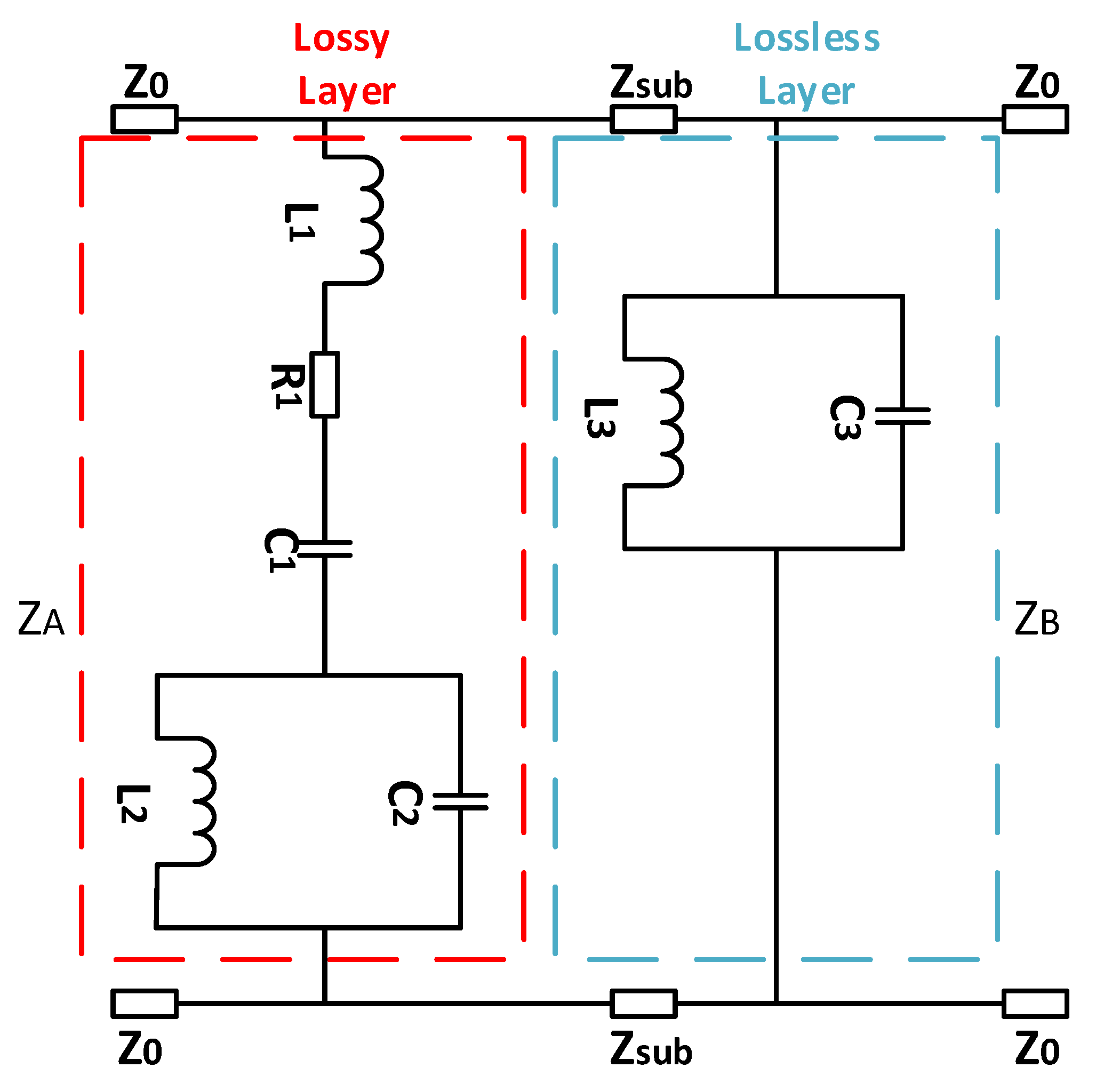
2. Basic Guidelines of the FSR

The ECM of a two-layer FSR structure is shown in Figure 1.   Z 0 and Z s u b denote the characteristic impedances of the free space and the dielectric spacer, respectively. Z A and Z B are the equivalent impedances of the lossy layer and the lossless layer, respectively. Z A is expressed as Z A = R 1 + j X R , and is a complex impedance due to its lossy properties. Z B is a pure reactance expressed as Z B = j X B .
According to the transmission line theory and the ECM depicted in Figure 1, the ABCD matrix is equal to the following [1]:
A B C D = 1 0 1 Z A 1 cos θ j Z s u b sin θ j sin θ Z s u b cos θ 1 0 1 Z B 1 = cos θ + j Z s u b Z B sin θ j Z s u b sin θ Z A + Z B Z A Z B cos θ + j 1 Z s u b + Z s u b Z A Z B sin θ cos θ + j Z s u b Z A sin θ
where θ = β t = 2 π λ   t , t is the thickness of the dielectric spacer.
Based on the scatter matrix and the analysis of the ECM [1], the reflection coefficient S 11   and the transmission coefficient S 21 can be written as follows:
S 11 = j Z s u b Z 0 Z 0 Z s u b Z A Z B Z 0 Z A + Z B tan θ + j Z s u b Z A Z 0 Z B j Z s u b Z 0 + Z 0 Z s u b Z A Z B + 2 Z A Z B + Z 0 Z A + Z B tan θ + j Z s u b Z A + Z 0 + Z B
S 21 = 2 Z A Z s u b Z B 2 Z A Z B + Z 0 Z A + Z 0 Z B Z s u b cos θ + j sin θ Z 2 s u b Z 0 + Z 0 Z A Z B + Z 2 s u b Z 0 + Z A + Z B
At the absorptive band, to reflect all incident power, the lossless layer should act as a metallic ground plane, so S 21 = 0 . Meanwhile, in order to make the design more feasible, foam is used as a dielectric spacer, which means that   Z s u b = Z 0 . Thus, the expression of S 11 can be calculated as
S 11 = Z 0 Z A cos θ + j Z 0 Z A Z 0 sin θ Z 0 Z A cos θ + j Z 0 Z A + Z 0 sin θ
At the same time, the transmission coefficient S 21 can be rewritten as follows:
S 21 = 2 2 + Z 0 Z A
From the equation, it can be seen that the larger Z A is, the closer the transmission coefficient is to one. The insertion loss decreases as the impedance Z A increases. When the resistor sheet is also in parallel resonance, an infinite value of Z A can be achieved, resulting in unity transmission. To realize a transmission passband, the parallel circuit L 2 C 2 and L 3 C 3 should resonate at the same frequency.

3. Design of the Switchable FSR

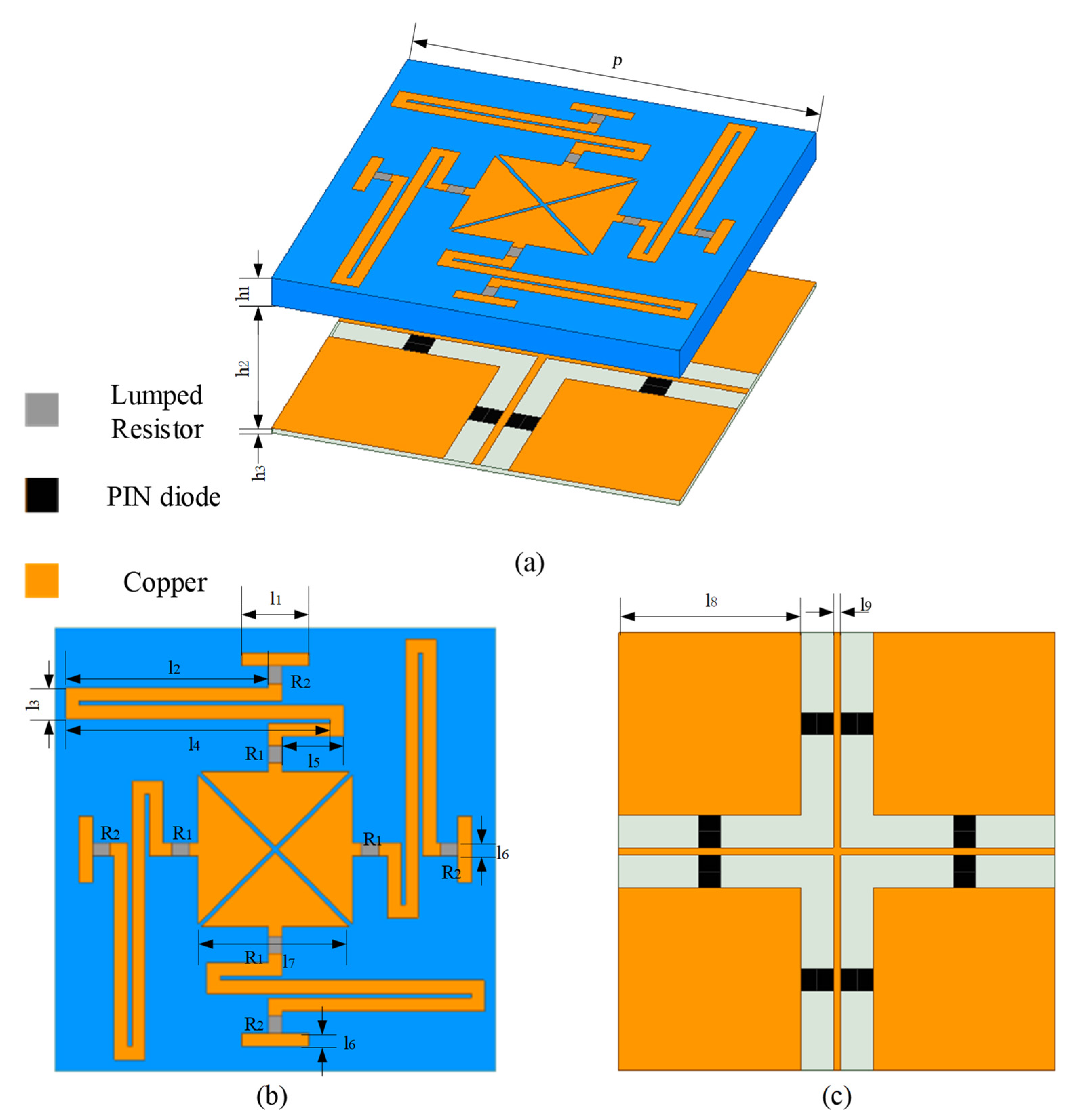
3.1. Design of the Proposed FSR

On the basis of the above analysis, the design of the proposed switchable FSR is illustrated in Figure 2. This switchable FSR consists of a lossless frequency-selective layer and a lossy wave-absorbing layer. In the unit structure of the switchable FSR, the lossy layer is composed of four triangular patches, four folded wires, and eight resistors which serve to absorb electromagnetic waves. The lossless layer consists of four square patches and cross-shaped patches, with eight sets of PIN diodes loaded in the middle of the crosses and squares, enabling the switchable function. The lossy layer is machined on a Rogers RT/duroid 5880 with a relative permittivity ɛ r of 2.2 while the lossless layer is processed on a Rogers RO3010 with ɛ r = 10.2 . The dimensions of the switchable FSR are as follows: p = 10.00   m m , l 1 = 1.50   m m , l 2 = 4.60   m m , l 3 = 0.70   m m , l 4 = 6.00   m m , l 5 = 1.40   m m , l 6 = 0.30   m m , l 7 = 3.35   m m , l 8 = 4.20   m m , l 9 = 0.20   m m , h 1 = 0.75   m m ,   h 2 = 3.375   m m , h 3 = 0.125   m m , R 1 = 40   Ω , and R 2 = 140   Ω . And the size of the PIN diode is 0.8   m m 0.6   m m .
The S-parameters of the switchable FSR, as simulated by the High-Frequency Structure Simulator (HFSS) under different polarizations, are shown in Figure 3. From the simulation results, it can be seen that for TE-polarized incident waves, when the PIN diodes are in the “ON” state, the passband with a −3 d B insertion loss for the switchable FSR ranges from 10.13 to 12.27 G H z and represents a fractional bandwidth of 19.11%. A transmission response occurs at around 11.44 G H z with an insertion loss of 1.94 d B . Additionally, the bandwidth for a reflection coefficient less than −10 d B extends from 5.79 to 15.37 G H z . Conversely, when the PIN diodes are switched “OFF”, the transmission from the switchable FSR falls well below −10 d B in the frequency range of 10.68 to 18.00 G H z . Meanwhile, when the TM-polarized wave is incident, its power is mostly equal to that of the TE wave. The simulation results indicate that the switchable FSR exhibits dual polarization. Whether the incident waves are TE or TM-polarized, the switchable FSR can be toggled between transmission and reflection modes.

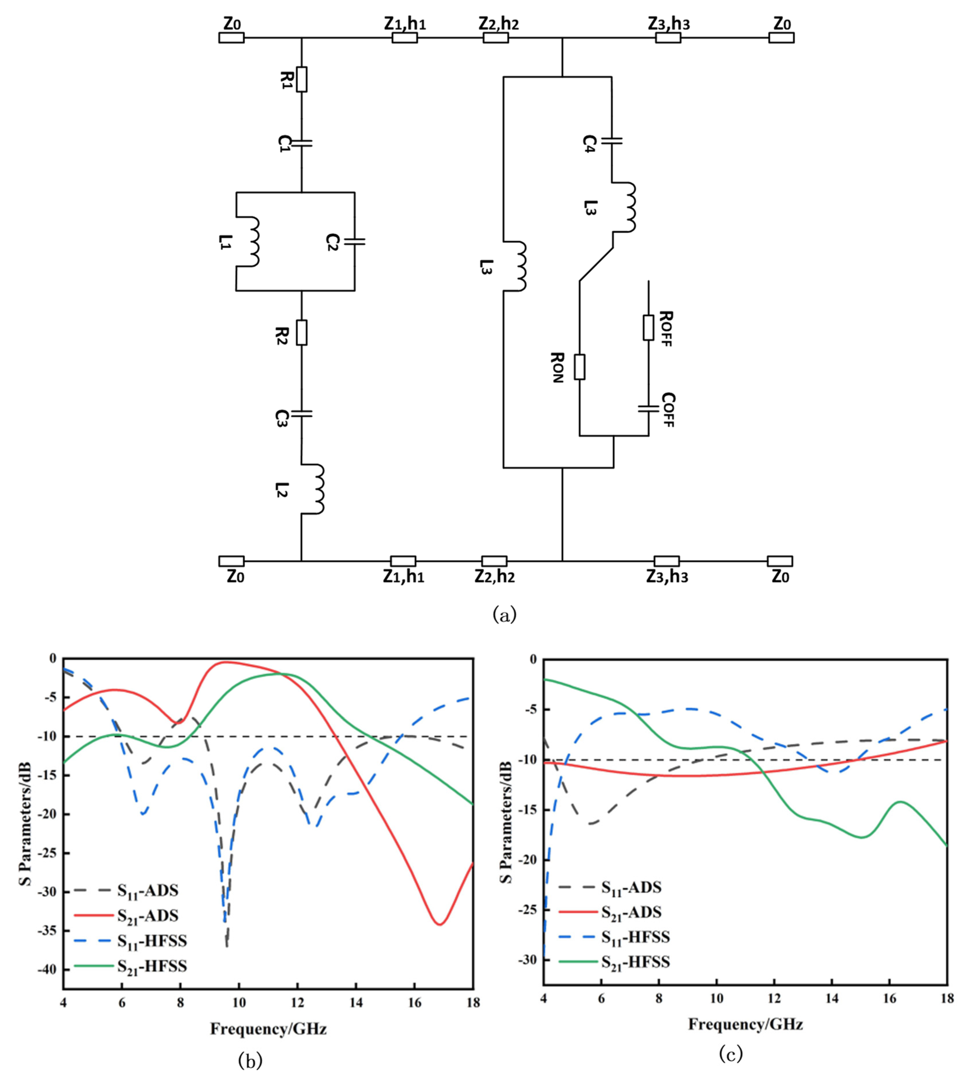
3.2. Equivalent Circuit Model

The complete ECM of the switchable FSR is given in Figure 4a. As can be seen in Figure 4a, the PIN diodes can be used as a device to control the switch. When the PIN diodes are in the ON state, they can be seen as a resistor. And when in the OFF state, they are a resistor and capacitor in a series. The reflection and transmission coefficients of the switchable FSR simulated by the HFSS and Advanced Design System (ADS) are shown in Figure 4b,c. The circuit simulation is conducted with the following optimized values:   Z 0 = Z 2 = 377   Ω , h 2 = 3.375   m m ,   Z 1 = 254   Ω ,   h 1 = 0.75   m m ,   Z 3 = 118   Ω ,   h 3 = 0.125   m m ,   R 1 = 60   Ω ,   C 1 = 0.04   p F ,   L 1 = 2.5   n H ,   C 2 = 0.1072   p F ,   R 2 = 140   Ω ,   C 3 = 0.2   p F ,   L 2 = 4.4   n H ,   L 3 = 2.83   n H ,   C 4 = 0.059   p F ,   L 4 = 1.5   n H ,   R O N = 10   Ω ,   R O F F = 1.5   k Ω , and C O F F = 0.1   p F . It can be observed from Figure 4b that the S 11 lower than −10 d B share the wide bandwidth from 7.47 to 14.22 G H z , with the exception of 7.46–8.83 G H z . Meanwhile, the passband with the −3 d B insertion loss of the switchable FSR is from 8.75 to 11.89 G H z . On the contrary, when the PIN diodes are in the OFF state, the transmission coefficient below −10 d B in the frequency range from 4.00 to 14.12 G H z can be seen. And the −10 d B transmission band covers from 4.21 to 9.94 G H z . It can be seen that the four lines roughly match. The difference between the two is that the ADS is an idealized model and the ECM is an approximation of the model structure. The difference may have a parasitic small inductive or capacitive effect. And at high frequencies, the effect of parasitic capacitance is stronger.

4. Analysis of the Switchable FSR

To explain the operating mechanism, the E-field and surface current distribution at 11.44 G H z for the switchable FSR are shown in Figure 5. As shown in Figure 5a, in the ON state, the electric field is mainly distributed in the X slit in the center, while a small portion of the current is also distributed along the folding lines. Meanwhile, regarding the current distribution, the current is present throughout the upper layers, but it is more intense along the upper-, right-, and lower-side folding lines. When the PIN diodes are switched OFF, the electric field is primarily distributed along the folding lines and X slits on the top and bottom sides, with the metal patches on the left and right sides also having a portion of the electric field. For the current distribution, it is evident that the current along the right-side folding line will be more pronounced, and the currents are also stronger on the left- and top-side folding lines.
The simulation results for the oblique incidence of the switchable FSR under different polarizations are depicted in Figure 6. For TE polarizations, as the oblique incidence angle reaches 15°, the switchable FSR displays a transmission window from 10.17 to 12.38 G H z with a minimum insertion loss under 2 d B in the ON state. Concurrently, an expansive absorption band from 6.10 to 16.07 G H z is observed. In the ON state for TM polarizations, the FSR offers a transmission band spanning 10.04 to 12.42 G H z and a reflection coefficient bandwidth below −10 d B from 6.12 to 15.84 G H z . However, in the OFF state for TE polarization, the transmission window vanishes, revealing an absorption band from 11.42 to 18.00 G H z . For TM polarization, the −10 d B absorption band ranges from 11.68 to 18.00 G H z . In the ON state and with oblique incidences up to 30° for TE polarizations, the 3 d B transmission band spans from 10.43 to 12.36 G H z , with a notable minimum insertion loss of 2.25 d B at 11.59 G H z . Excluding the range of 10.91–11.72 G H z , the working bands have S 11 < −10 d B from 6.10 to 16.02 G H z . For TM polarizations, the measured 3 d B transmission bands extend from 9.86 to 10.68 G H z and 11.29 to 12.56 G H z , with the working band exhibiting S 11 < −10 d B across 6.33–16.97 G H z . In contrast, with the PIN diodes in the OFF state, the transmission coefficient falls below −10 d B in the 11.23 to 18.00 G H z frequency range under TE polarization. The −10 d B transmission band for TM polarization spans from 12.27 to 18.00 G H z . For oblique incidences reaching 40° under TE polarizations in the ON state, the transmission window, with an insertion loss below 3 d B , lies between 10.93 and 12.26 G H z . The reflection coefficient below −10 d B (| S 11 | < −10 d B ) covers the 6.13 to 14.28 G H z range, excluding 7.99–8.70 G H z and 10.72–12.17 G H z . For TM polarizations, transmission bands of 9.69–10.72 G H z and 11.48–12.65 G H z are observed, with an insertion loss below 3 d B . Additionally, the −10 d B absorption band covers 6.50–18.00 G H z , save for the 12.02 to 12.77 G H z range. In the OFF state, the passband vanishes, presenting a wide low-reflection band from 10.88 to 18.00 G H z under TE polarization. The −10 d B bands under TM polarization extend from 13.12 to 18.00 G H z . Overall, the results indicate stable transmission characteristics for incidence angles ranging from 0° to 40° across both TE and TM polarizations.
To elucidate the advantages of the proposed FSR, Table 1 presents a comparison with recently reported FSR structures. It is evident from the table that the −3 d B transmission band of this structure is the widest, ranging from 10.13 to 12.27 G H z , marking it as the broadest FSR currently in the X-band. One drawback, however, is that the insertion loss is somewhat high. This is partly due to a portion of the transmittance being sacrificed to increase the transmittance band bandwidth, and partly because of the loss caused by the resonance within the resistance layer. Simultaneously, the operating bandwidth spans from 5.79 to 15.37 G H z , with a relative bandwidth of 91%. Additionally, the FSR is insensitive to both transverse and longitudinal electromagnetic waves and can ensure the passage of electromagnetic waves within a 0–40° range. As the FSR constitutes a periodic structure, it is dual-polarized.

5. Conclusions

In conclusion, we present a dual-polarized FSR that can switch between a passband and a reflection band within the X-band. Initially, we analyze the basic FSR circuit model and propose a switchable FSR model. The lossy layer of this model consists of four triangular patches and their corresponding folded lines, while the lossless layer is composed of square and cross metal patches, with PIN diodes loaded between them. Subsequently, we simulate the proposed FSR, establish its ECM, and analyze its working state. The simulation results reveal that, when the PIN diodes are in the ON state, the 3 d B transmission band of the proposed switchable FSR covers the range from 10.13 to 12.27 G H z . This represents the broadest coverage among all the switchable FSRs published to date. A minimum insertion loss of 1.94 d B is obtained at 11.44 G H z , and the working bands with S 11 < −10 d B range from 5.79 to 15.37 G H z . On the contrary, when the PIN diodes are in the OFF state, the transmission coefficient below −10 d B in the frequency range from 10.68 to 18.00 G H z can be seen. The development of this switchable FSR holds significant implications for the advancement of stealth technology.

Author Contributions

Conceptualization, S.S. and Z.C.; methodology, S.S.; software, Z.C.; validation, S.Z., Y.S. and Y.Z.; formal analysis, Z.C.; investigation, S.S.; resources, S.S.; data curation, S.Z.; writing—original draft preparation, S.S.; writing—review and editing, S.S., Y.S. and Y.Z.; visualization, Z.C.; supervision, Y.S. and Y.Z.; project administration, S.S.; funding acquisition, Y.S. All authors have read and agreed to the published version of the manuscript.

Funding

This work was supported in part by the Natural Science Foundation of Shandong Province under Grant ZR2019BF014.

Data Availability Statement

Not applicable.

Conflicts of Interest

The authors declare no conflict of interest.

References

  1. Munk, B.A. Frequency Selective Surfaces: Theory and Design; John Wiley & Sons: Hoboken, NJ, USA, 2005. [Google Scholar]
  2. Arceneaux, W.S.; Akins, R.D.; May, W.B. Absorptive/Transmissive Radome. U.S. Patent US5400043A, 21 March 1995. [Google Scholar]
  3. Munk, B.A. Metamaterials: Critique and Alternatives; John Wiley & Sons: Hoboken, NJ, USA, 2009. [Google Scholar]
  4. Kiani, G.I.; Esselle, K.P.; Ford, K.L.; Weily, A.R.; Panagamuwa, C. Angle and polarization-independent bandstop frequency selective surface for indoor wireless systems. Microw. Opt. Technol. Lett. 2008, 50, 2315–2317. [Google Scholar] [CrossRef]
  5. Kiani, G.I.; Ford, K.L.; Esselle, K.P.; Weily, A.R.; Panagamuwa, C.J. Oblique incidence performance of a novel frequency selective surface absorber. IEEE Trans. Antennas Propag. 2007, 55, 2931–2934. [Google Scholar] [CrossRef]
  6. Kiani, G.I.; Weily, A.R.; Esselle, K.P. Frequency selective surface absorber using resistive cross-dipoles. In Proceedings of the 2006 IEEE Antennas and Propagation Society International Symposium, Albuquerque, Mexico, 9–14 July 2006; pp. 4199–4202. [Google Scholar]
  7. Motevasselian, A.; Jonsson, B.L.G. Design of a wideband rasorber with a polarisation-sensitive transparent window. IET Microw. Antennas Propag. 2012, 6, 747–755. [Google Scholar] [CrossRef]
  8. Motevasselian, A.; Jonsson, B.L.G. Partially transparent Jaumann-like absorber applied to a curved structure. Int. J. Antennas Propag. 2011, 2011, 708987. [Google Scholar] [CrossRef]
  9. Li, B.; Shen, Z. Wideband 3D frequency selective rasorber. IEEE Trans. Antennas Propag. 2014, 62, 6536–6541. [Google Scholar] [CrossRef]
  10. Shen, Z.; Wang, J.; Li, B. 3-D frequency selective rasorber: Concept, analysis, and design. IEEE Trans. Microw. Theory Tech. 2016, 64, 3087–3096. [Google Scholar] [CrossRef]
  11. Chen, Q.; Yang, S.; Bai, J.; Fu, Y. Design of absorptive/transmissive frequency-selective surface based on parallel resonance. IEEE Trans. Antennas Propag. 2017, 65, 4897–4902. [Google Scholar] [CrossRef]
  12. Han, Y.; Che, W.; Xiu, X.; Yang, W.; Christopoulos, C. Switchable low-profile broadband frequency-selective rasorber/absorber based on slot arrays. IEEE Trans. Antennas Propag. 2017, 65, 6998–7008. [Google Scholar] [CrossRef]
  13. Xia, J.; Wei, J.; Liu, Y.; Zhang, Y.; Guo, S.; Li, C.; Bie, S.; Jiang, J. Design of a wideband absorption frequency selective rasorber based on double lossy layers. IEEE Trans. Antennas Propag. 2020, 68, 5718–5723. [Google Scholar] [CrossRef]
  14. Bouslama, M.; Traii, M.; Denidni, T.A.; Gharsallah, A. Beam-Switching Antenna with a New Reconfigurable Frequency Selective Surface. IEEE Antennas Wirel. Propag. Lett. 2016, 15, 1159–1162. [Google Scholar] [CrossRef]
  15. Fan, J.; Chen, W.; Chen, D.; Chen, H.; Luo, L.; Bao, S. Vibro-acoustic modulation-based bolt looseness detection method using frequency sweep probe waves. Nondestruct. Test. Eval. 2023, 1–22. [Google Scholar] [CrossRef]
  16. Marindra, A.M.J.; Tian, G.Y. Chipless RFID sensor for corrosion characterization based on frequency selective surface and feature fusion. Smart Mater. Struct. 2020, 29, 125010. [Google Scholar] [CrossRef]
  17. Daura, L.U.; Tian, G.Y. Characterization of Angular RCF Cracks in a Railway Using Modified Topology of WPT-Based Eddy Current Testing. IEEE Trans. Ind. Inform. 2023, 19, 5612–5622. [Google Scholar] [CrossRef]
  18. Costa, F.; Monorchio, A. A frequency selective radome with wideband absorbing properties. IEEE Trans. Antennas Propag. 2012, 60, 2740–2747. [Google Scholar] [CrossRef]
  19. Costa, F.; Monorchio, A. Absorptive frequency selective radome. In Proceedings of the 2011 XXXth URSI General Assembly and Scientific Symposium, Istanbul, Turkey, 13–20 August 2011; pp. 1–4. [Google Scholar]
  20. Liu, L.G.; Li, Y.Q.; Meng, Q.Z.; Wu, W.W.; Mo, J.J.; Fu, Y.Q.; Yuan, N.C. Design of an invisible radome by frequency selective surfaces loaded with lumped resistors. Chin. Phys. Lett. 2013, 30, 064101. [Google Scholar] [CrossRef]
  21. Shang, Y.; Shen, Z.; Xiao, S. Frequency-selective rasorber based on square-loop and cross-dipole arrays. IEEE Trans. Antennas Propag. 2014, 62, 5581–5589. [Google Scholar] [CrossRef]
  22. Huang, H.; Shen, Z. Absorptive frequency-selective transmission structure with square-loop hybrid resonator. IEEE Antennas Wirel. Propag. Lett. 2017, 16, 3212–3215. [Google Scholar] [CrossRef]
  23. Guo, M.; Chen, Q.; Sun, Z.; Sang, D.; Fu, Y. Design of dual-band frequency-selective rasorber. IEEE Antennas Wirel. Propag. Lett. 2019, 18, 841–845. [Google Scholar] [CrossRef]
  24. Li, B.; Shen, Z. Three-Dimensional Bandpass Frequency-Selective Structures with Multiple Transmission Zeros. IEEE Trans. Microw. Theory Tech. 2013, 61, 3578–3589. [Google Scholar] [CrossRef]
  25. Yu, W.; Luo, G.Q.; Yu, Y.; Liao, Z.; Jin, H.; Shen, Z. Broadband Band-Absorptive Frequency-Selective Rasorber with a Hybrid 2-D and 3-D Structure. IEEE Antennas Wirel. Propag. Lett. 2019, 18, 1701–1705. [Google Scholar] [CrossRef]
  26. Yu, Y.; Deng, T.; Shen, Z. Wideband 3D frequency selective rasorber with two absorption bands. In Proceedings of the 2016 11th International Symposium on Antennas, Propagation and EM Theory (ISAPE), Guilin, China, 18–21 October 2016. [Google Scholar]
  27. Omar, A.A.; Shen, Z.; Huang, H. Absorptive Frequency-Selective Reflection and Transmission Structures. IEEE Trans. Antennas Propag. 2017, 65, 6173–6178. [Google Scholar] [CrossRef]
  28. Wang, Y.; Qi, S.S.; Shen, Z.; Wu, W. Ultrathin 3-D frequency selective rasorber with wide absorption bands. IEEE Trans. Antennas Propag. 2020, 68, 4697–4705. [Google Scholar] [CrossRef]
  29. Wang, Y.; Wang, M.; Shen, Z.; Wu, W. 3-D Single- and Dual-Polarized Frequency-Selective Rasorbers with Wide Absorption Bands Based on Stepped Impedance Resonator. IEEE Access 2021, 9, 22317–22327. [Google Scholar] [CrossRef]
  30. Wu, L.; Zhong, S.; Huang, J.; Liu, T. Broadband frequency-selective rasorber with varactor-tunable interabsorption band transmission window. IEEE Trans. Antennas Propag. 2019, 67, 6039–6050. [Google Scholar] [CrossRef]
  31. Guo, M.; Chen, Q.; Zheng, Y.; He, Y.; Fu, Y. Continuous Tunable Transmission Band Frequency Selective Rasorber Radome with Inter-Absorption Band Based on Varactor. In Proceedings of the 2019 8th Asia-Pacific Conference on Antennas and Propagation (APCAP), Incheon, Korea, 4–7 August 2019; pp. 326–328. [Google Scholar]
  32. Bakshi, S.C.; Mitra, D.; Teixeira, F.L. Wide-angle broadband rasorber for switchable and conformal application. IEEE Trans. Microw. Theory Tech. 2021, 69, 1205–1216. [Google Scholar] [CrossRef]
  33. Qian, G.; Zhao, J.; Ren, X.; Chen, K.; Jiang, T.; Feng, Y.; Liu, Y. Switchable broadband dual-polarized frequency-selective rasorber/absorber. IEEE Antennas Wirel. Propag. Lett. 2019, 18, 2508–2512. [Google Scholar] [CrossRef]
  34. Li, R.; Tian, J.; Jiang, B.; Lin, Z.; Chen, B.; Hu, H. A switchable frequency selective rasorber with wide passband. IEEE Antennas Wirel. Propag. Lett. 2021, 20, 1567–1571. [Google Scholar] [CrossRef]
  35. Tang, M.; Zhou, D.F.; Liu, Q.K.; Yao, Z.N.; Liu, Q. Low-profile FSS-based polarization-insensitive rasorber with switchable transmission band. IEEE Antennas Wirel. Propag. Lett. 2021, 20, 1038–1042. [Google Scholar] [CrossRef]
  36. Dutta, R.; Ghosh, J.; Sarkhel, A. Planar Frequency Selective Surface-Based Switchable Rasorber/Absorber for Airborne Application. IEEE Antennas Wirel. Propag. Lett. 2022, 21, 1842–1846. [Google Scholar] [CrossRef]
  37. Wang, H.; Kong, X.; Zhang, X. A Dual-Polarized Frequency-Selective Rasorber With a Switchable Wide Passband Based on Characteristic Mode Analysis. Front. Mater. 2022, 9, 912913. [Google Scholar] [CrossRef]
  38. Yang, X.L.; Liu, Z.G.; Chen, H.; Geng, M.Y.; Bo, X.Z.; Lu, W.B. Switchable Rasorber/Absorber with Frequency Tuning Capability. In Proceedings of the 2022 IEEE MTT-S International Microwave Workshop Series on Advanced Materials and Processes for RF and THz Applications (IMWS-AMP), Guangzhou, China, 27–29 November 2022; pp. 1–3. [Google Scholar]
  39. Wu, Z.; Zhou, Q.; Liu, P.; Lin, M. Active Frequency Selective Rasorber with Switchable Transmission Band and Tunable Absorption Band. IEEE Microw. Wirel. Technol. Lett. 2023, 33, 1247–1250. [Google Scholar] [CrossRef]
Figure 1. General ECM of the dual-layer FSR.
Electronics 12 03941 g001
Figure 2. (a) The structure of the proposed FSR; (b) the top of the FSR; (c) the bottom of the FSR.
Electronics 12 03941 g002
Figure 3. The simulated results of the switchable FSR obtained from HFSS under different incidences: (a) when PIN diodes are in the ON state; (b) when PIN diodes are in the OFF state.
Electronics 12 03941 g003
Figure 4. (a) The ECM of the switchable FSR; (b) the S-Parameters of the switchable FSR calculated by ADS and HFSS when PIN diodes are in the ON state; (c) the S-Parameters of the switchable FSR calculated by ADS and HFSS when PIN diodes are in the ON state.
Electronics 12 03941 g004
Figure 5. The E-field and surface current distribution at 11.44 GHz of the switchable FSR with (a) the E-field distribution in the ON state; (b) the surface current distribution in the ON state; (c) the E-field distribution in the OFF state; and (d) the surface current distribution in the OFF state.
Electronics 12 03941 g005
Figure 6. Scattering parameters of the switchable FSR under oblique incidence with (a) diode ON under TE polarization; (b) diode OFF under TE polarization; (c) diode ON under TM polarization; and (d) diode OFF under TM polarization.
Electronics 12 03941 g006
Table 1. Comparisons between the switchable FSR and previously reported FSRs.
Ref.Realization of Lossy FSS The 3   d B   Transmission   Bandwidth   ( G H z ) Insertion   Loss   ( d B ) FBW   ( S 11 < 10 d B )Oblique PerformancePolarization
[33]a square loop, the center patch metallic parts1.61.7124%30°dual
[34]the dual-spiral structure1.1<167%45°dual
[35]the parallel outer loop and inner rectangles0.80.35112%40°dual
[36]the outer and inner square
loop
20.2103%30°single
This workthe four triangular patches and four folded wires2.141.9491%4dual
Disclaimer/Publisher’s Note: The statements, opinions and data contained in all publications are solely those of the individual author(s) and contributor(s) and not of MDPI and/or the editor(s). MDPI and/or the editor(s) disclaim responsibility for any injury to people or property resulting from any ideas, methods, instructions or products referred to in the content.

