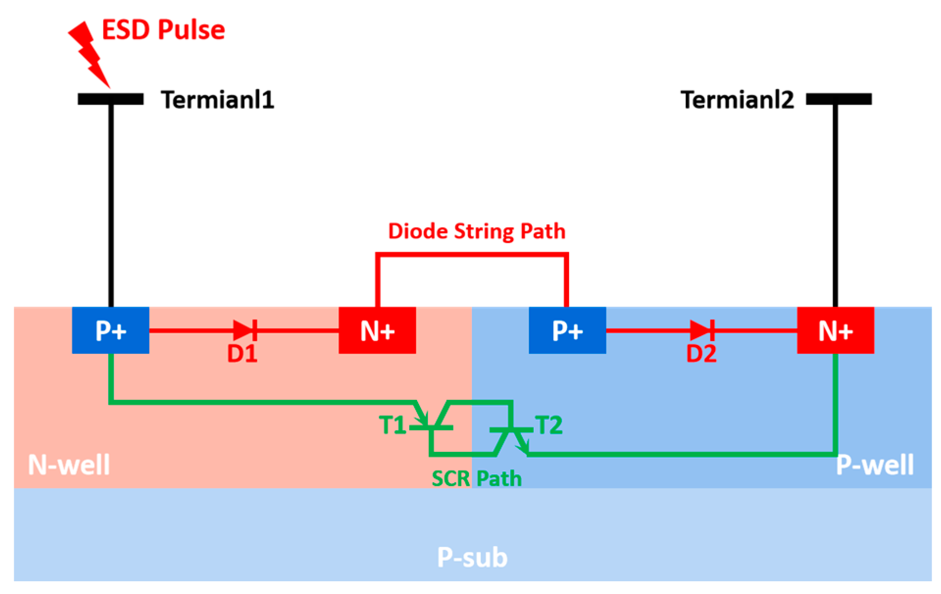
Article

High Area Efficiency Bidirectional Silicon-Controlled Rectifier for Low-Voltage Electrostatic Discharge Protection

1
Key Laboratory of Micro-Nano Electronic Devices and Smart Systems of Zhejiang Province, College of Information Science & Electronic Engineering, Zhejiang University, Hangzhou 310027, China
2
Beijing Smart-chip Microelectronics Technology Co., Ltd., Beijing 102299, China
3
ZJU-Hangzhou Global Scientific and Technological Innovation Center, Zhejiang University, Hangzhou 311215, China
*
Authors to whom correspondence should be addressed.
These authors contributed equally to this work.
Electronics 2023, 12(19), 4011; https://doi.org/10.3390/electronics12194011
Submission received: 30 August 2023 / Revised: 16 September 2023 / Accepted: 19 September 2023 / Published: 23 September 2023
(This article belongs to the Special Issue Advances of Electronics Research from Zhejiang University)

Abstract

:
Continuously scaling down and decreasing operation voltages of ICs, from the 5 V TTL-compatible voltage to 3.3 V, then 1.2 V, and now 0.8 V for low-power ICs, results in more stringent electrostatic discharge protection design requirements, such as a narrow ESD design window, low operation voltage, and high ESD robustness. Based on traditional diode string and diode-triggered silicon-controlled rectifiers, an enhanced diode-triggered silicon-controlled rectifier is proposed to meet the requirements of low-voltage integrated circuits as bidirectional electrostatic discharge protection. The new device employs an additional PMOS and NMOS in the N-well and P-well, respectively, to offer additional current paths along the surface to significantly enhance its robustness. TCAD simulation shows that the device is triggered by both the diode strings and embedded MOS, making the device turn on faster and the current distribution more uniform during the ON state owing to the additional surface current paths. The proposed new device has excellent dual-directional ESD protection performance with a figure of merit of 4.01 mA/um2, which is about a 71% improvement compared with the conventional diode-triggered silicon-controlled rectifier. It also has higher area efficiency, lower trigger voltage, lower current leakage, and a faster turn-on speed. The proposed enhanced diode-triggered silicon-controlled rectifier is an attractive ESD protection solution for ultra-low-voltage ICs.

1. Introduction

Electrostatic discharge (ESD) is the major cause of IC failure in manufacturing, transportation, PCB mounting, and the operation of electronic products [1]. With the development of ultra-low-power integrated circuits, the operation voltage has been down-scaled continuously from the 5 V TTL-compatible voltage to 3.3 V, then 1.2 V, and now 0.8 V for low-power ICs [2,3,4,5]. A bidirectional ESD device is needed for protecting pins with an operating voltage varying between positive and negative values, and a bidirectional silicon-controlled rectifier (BSCR) capable of operating in the NS and PS modes of ESD stresses is suitable for such an application [6]. Though bidirectional ESD protection based on a simple back-to-back diode string has a good area efficiency ratio and a low trigger voltage under a positive bias state, it easily results in a large turn-on resistance (Ron) and leakage current at the PN junction [7]. A diode-triggered SCR (DTSCR) can improve the ESD robustness and reduces the ON resistance [8,9], but it requires a parallel connection of two opposing-polarity one-directional DTSCRs to conduct both positive and negative ESD currents. The BDTSCR proposed by Liu et al. [10] and the BLVSCR proposed by Du et al. [11] realized dual-directional ESD protection, but the large Vt1 and ON resistance restrict their practical application. F. Du et al. prepared a fast turn-on speed DTSCR by embedding current gain amplifier modules, but its ESD robustness still needs to be improved [11]. A high-performance bidirectional ESD protection scheme for ultra-low-power integrated circuits has yet to be developed. In this paper, we propose an enhanced diode-triggered silicon-controlled rectifier (EDTSCR). As will be demonstrated later, the new device structure has a high area efficiency, low turn-on resistance, and high turn-on speed due to the gate-coupling effect of MOS, which leads to an increased skin effect of the current and a reduced response time.

2. New ESD Device Structure

A cross-sectional view and an equivalent schematic of the conventional DTSCR device structure are illustrated in Figure 1. There are two conduction paths in the DTSCR. The first path is illustrated in red and is via the diode string constituted by PN diodes D1 and D2. The second path, drawn in green, is the SCR path formed by two bipolar junction transistors (BJTs), T1 and T2. In general, the DTSCR is triggered by the diode string path first, and when the ESD stress increases, the parasitic BJTs are turned on, forming a positive feedback to drain a large amount of the ESD current.
Figure 2 illustrates an improved DTSCR, the MDTSCR. Compared with the conventional DTSCR, the MDTSCR has an extra highly doped P+ region in the N-well and a highly doped N+ region in the P-well, which enables a bidirectional but not symmetrical ESD protection structure. Similar to the DTSCR, there are two additional conduction paths. The first path is the trigger path, constituted by the diode strings, which are marked in red. The second conduction path passes via the SCR (T1 and T2) together with transistors T3 or T4, depending on the ESD strike direction. The parasitic SCR in a positive ESD strike is the main current conduction path, but under negative ESD stress, due to the extension of the SCR path, a partial ESD current is also discharged through both the PNP path and NPN path according to the principle that a current always takes a path with less impedance, which results in a larger ON resistance and worse ESD robustness.
Here, we further improved the ESD performance of the DTSCR above that of the MDTSCR. As shown in Figure 3, we incorporated two highly doped P+ regions on the surface of the N-well. It forms a PMOS on the surface. Similarly, two N+ regions were inserted into the P-well to form an additional NMOS. The gates of the introduced PMOS and NMOS were connected together. Similar to the MDTSCR, the current conduction of the EDTSCR is bidirectional, and it is an inverter with an intrinsic LU structure where the wells and gates are shorted. However, in addition to parasitic BJT paths (T3 and T4) in the bulk, the EDTSCR offers an additional surface conduction path via the newly incorporated MOS transistors, M1 and M2. The gates of the PMOS and NMOS were connected together. As demonstrated in Figure 3b,d, due to the gate coupling effect, the majority carrier at the channel will be depleted first, and then the minority carrier will accumulate on the channel surface to form an inversion layer so that when an ESD pulse is applied, the MOS structure will turn on quickly and offer additional current paths. Nevertheless, the MOS path current mainly depends on the channel length, where the longer channel length is, the greater gate capacitance and channel resistance are, and less current can be conducted. Moreover, triggered by the diode string, the turn-on voltage of the EDTSCR is basically the same as that of the above devices, but in the same way, the parasitic SCR conduction path in the EDTSCR is shorter than that of a negative ESD pulse strike because of the asymmetrical device structure. Therefore, a fair portion of the ESD current is also discharged through both the PNP path and NPN path under negative ESD stress, and its positive characteristics of a stronger ESD robustness and lower ON resistance can also be expected.
All of these devices, DTSCR, MDTSCR, and EDTSCR, have the same width and length. In Section 3, the bidirectional turn-on process of the EDTSCR will be analyzed based on the TCAD simulation. And in Section 4, the performance of all devices with the same area will be tested to verify the superior characteristics of the newly proposed EDTSCR.

3. TCAD Simulation

The operation mechanisms of the EDTSCR under both positive and negative ESD strikes were validated by the 2D TCAD simulations. As shown in Figure 4, the impurity concentration profiles of the EDTSCR were inferred from the process simulation results, while analytical functions were used to easily consider layout variations of the investigated structures. All simulations were carried out using the drift-diffusion model coupled with the heat-transfer equation. Shockley–Read–Hall and Auger generation–recombination models were used along with the Unibo impact-ionization model. Thermoelectric simulations were carried out with ideal thermal boundary conditions, assuming room temperature at the metal contacts. An electrical stress of a ±30 V pulse with a 10 ns raise time and 100 ns width was used in the current density simulation.

3.1. Bidirectional Turn-on Process

According to the simulated current density distribution at 1 ns, shown in Figure 5, it was confirmed that the bidirectional EDTSCR is triggered by diode strings with two forward PN junctions and parasitic resistance in both the N-well and P-well. This trigger mechanism leads to a low trigger voltage of about 1.4 V.
When the positive input voltage increased with the pulse rising edge, the positive feedback of the SCR formed at 3 ns and most of the current began to flow from the anode to the cathode through the SCR path, shown in Figure 6a. While under negative ESD stress, the lengths of the PNP, NPN, and SCR paths are too long to participate in current conduction, and thus the ESD current still preferred to drain from the diode string path, as shown in Figure 6b. In addition, an initial channel current was also generated because of the gate coupling effect under both positive and negative ESD stress.
When the device was completely in ON mode at 10 ns, both the SCR and MOS, including their channel paths and parasitic BJTs, discharged current together under positive ESD stress, as shown in Figure 7a. However, in a negative strike, the parasitic PNP and NPN in the MOS transistors destroyed the positive feedback needed for SCR path formation so that the PNP and NPN paths were the main discharge paths at 10 ns, while partial current still flowed through the MOS channel and the diode string path, as shown in Figure 7b.
In general, the turn-on process of the EDTSCR can be summarized as follows:
For the positive ESD strike, as the trigger structure of the EDTSCR, current flows through the diode string path first at a low trigger voltage of about 1.4 V. When the input current increases, the positive feedback of the SCR forms and the parasitic SCR in the body replaces the diode string as the main discharge path. Finally, when completely in ON mode, both channel paths and parasitic BJTs in the MOS transistors are turned on, and now multiple paths participate in ESD current conduction, resulting in a lower ON resistance and stronger robustness.
For the negative ESD strike, the diode string path is still the trigger structure. But the presence of the PNP and NPN paths destroys the positive feedback needed for SCR path formation so that when the current increases gradually, the PNP and NPN paths always dominate the conduction of the ESD current. The lack of the SCR discharge path results in a larger ON resistance, higher snapback voltage, and lower failure current.

3.2. Gate Coupling Effect

In order to better understand the role of the gate coupling effect, the embedded NMOS and PMOS in the EDTSCR were simulated specifically. As shown in Figure 8, the channel current of the surface complementary NMOS and PMOS pair was significantly larger than the parasitic BJT current in both directions at 3 ns due to the gate coupling effect, explained in detail in Section 2, and this indicates that the EDTSCR will have a smaller ON resistance than the MDTSCR because of the existence of the additional MOS channel conduction paths. And, the simulation result also shows that this conduction path can make the current distribution more uniform and, hence, improve the robustness of the device.
In the TACD simulation, the channel currents at different moments (1 ns to 5 ns) were also studied. As shown in Figure 9a, the distribution of the embedded NMOS channel current was extracted along the tangent line in the Z direction. According to the simulation results in Figure 9b, with the addition of the diode string path, the charge accumulates rapidly on the channel surface to form an inversion layer at 1 ns, offering another MOS path. It is worth noting that the total current density at 1 ns was 8.2 × 10⁵ A*cm−2, and the individual MOS channel current density accounted for about 20%. Therefore, the embedded MOS structure, which is involved in the triggering process, contributes to the quick response of the device. Moreover, as the rising voltage caused a boost, the parasitic BJT also started to work, and the current density in the Z direction increased with time.
The channel length L is one of the key parameters of the EDTSCR, and the percentage of channel current with different channel lengths to the total current along the tangent line in the Z direction was calculated. As shown in Figure 10a, when triggered was at 1 ns, the shorter the channel length was, the larger the channel current proportion was due to the smaller gate capacitance, making the channel path easier to generate. After the device was triggered at 3 ns, as shown in Figure 10b, the channel current ratios of the different channel lengths L = 0.5 / 1.0 / 1.5   µ m were 10.5%, 9.2%, and 7.4%, which are all approximately the same.

4. Test Results

The DTSCR, MDTSCR, and EDTSCR were fabricated in a commercial 0.35-μm CMOS process with the same total width of 100 μm. The TLP measurements were conducted with the Barth 4002 TLP standard test system by using the human body model parameters with a 10 ns rising time and a 100 ns pulse width. Its setup is illustrated in Figure 11. For each voltage pulse, current and voltage waveforms were captured by using a 10 GHz oscilloscope. By averaging over 70–90% time windows of the stress pulse waveform, a single data point of I-V characteristics was extracted. This was followed by a low 0.5 V bias DC test at room temperature to confirm device failure.
The test results of the DTSCR, MDTSCR, and EDTSCR are illustrated in Figure 12, where the current is normalized. The curves with solid symbols represent the current–voltage (I-V) characteristics, and the curves with empty symbols are the leakage current characteristics. In general, the leakage current of the EDTSCR (empty round markers) was around 10−9, which is slightly larger than that of the MDTSCR or DTSCR.
Table 1 summarizes the major performance indicators for the DTSCR, MDTSCR, and EDTSCR in positive (pos) and negative (neg) ESD strikes. In general, due to the existence of the additional MOS channel conduction paths, the EDTSCR shows much higher second failure current (It2) values and smaller ON resistance (Ron) values than the DTSCR and MDTSCR under both positive and negative stress. The figure of merit (FOM), defined as the failure current per unit area, of the EDTSCR shows a near 71% improvement over the DTSCR and a 29% improvement over the MDTSCR in a positive ESD strike. Meanwhile, both the MDTSCR and EDTSCR at the positive strike achieved a stronger ESD robustness than the negative ones because the presence of the PNP and NPN paths destroys the positive feedback needed for SCR formation so that when the current increases gradually, the PNP and NPN paths always dominate the conduction of the ESD current instead of the SCR path. The FOM of the positive EDTSCR shows a near 27% advantage over the negative one.
To verify the turn-on speed of the EDTSCR, similar VFTLP measurements were also conducted with a 200 ps rising time and a 1 ns pulse width. The transient voltage waveforms of the DTSCR, MDTSCR, and EDTSCR under a 100 V positive VFTLP pulse are compared in Figure 13. According to the test results, the DTSCR and MDTSCR had almost consistent waveforms, with the same voltage overshoot of 4.80 V. But for the EDTSCR, as shown in the TCAD simulation results, the introduced MOS structure and gate coupling effect benefitted the low trigger voltage and quick response [12]. When the EDTSCR was turned on, its transient voltage peaked at 240 ps while both the DTSCR and MDTSCR peaked at 300 ps, which means that the EDTSCR had a lower voltage overshoot of 4.25 V and a faster turn-on ability.

5. Conclusions

In short, the newly proposed bidirectional EDTSCR ESD protection is based on the DTSCR structure with two additional NMOS and PMOS, which form a surface conduction path. The operation mechanisms of the device were confirmed with TCAD simulations. On account of the multiple additional conduction paths, including parasitic BJT paths and MOS channel paths due to the gate coupling effect, the EDTSCR has several advanced features, such as a low ON resistance, higher FOM, and faster turn-on speed. The channel length L is one of the key parameters of the EDTSCR. A longer channel length means that less channel current is involved in the triggering of the device, so the device turn-on speed and robustness will decrease due to the lack of a MOS discharge path. The EDTSCR should be a promising ESD protection solution for low-power IC applications.

Author Contributions

Conceptualization, S.D.; Methodology, D.Z., S.Z., F.G., Y.Y., Y.H., T.Z. and X.L.; Investigation, X.Z.; Writing—original draft, Y.C. All authors have read and agreed to the published version of the manuscript.

Funding

This research was funded by The Laboratory Open Fund of Beijing Smart-chip Microelectronics Technology Co., Ltd., grant number SGSC0000MNQT2207165.

Data Availability Statement

The data that support the findings of this study are available from the corresponding author, S.D., upon reasonable request.

Conflicts of Interest

The authors declare no conflict of interest.

References

  1. Dong, A.; Xiong, J.; Mitra, S.; Liang, W.; Gauthier, R.; Loiseau, A. Comprehensive Study of ESD Design Window Scaling Down to 7nm Technology Node. In Proceedings of the 40th Electrical Overstress/Electrostatic Discharge Symposium (EOS/ESD), Reno, NV, USA, 23–27 September 2018; pp. 1–8. [Google Scholar] [CrossRef]
  2. Jizhi, L.; Yaohui, Z.; Zhiwei, L.; Jianming, Z.; Hui, C.; Nie, L. Low-voltage triggering SCRs for ESD protection in a 0.35 μm SiGe BiCMOS process. Microelectron. Reliab. 2017, 73, 122–128. [Google Scholar] [CrossRef]
  3. Du, F.; Hou, F.; Song, W.; Chen, L.; Nie, Y.; Qing, Y.; Xu, Y.; Liu, J.; Liu, Z.; Liou, J.J. An Improved Silicon-Controlled Rectifier (SCR) for Low-Voltage ESD Application. IEEE Trans. Electron Devices 2020, 67, 576–581. [Google Scholar] [CrossRef]
  4. Gao, Y.; Cai, X.; Han, Z.; Zeng, C.; Xia, R.; Tang, Y.; Gao, M.; Li, B. Design of compact-diode-SCR with low-trigger voltage for full-chip ESD protection. Microelectron. Reliab. 2023, 140, 114860. [Google Scholar] [CrossRef]
  5. He, L.; Salcedo, J.A.; Parthasarathy, S.; Hajjar, J.-J.; Sundaram, K. A New Low-Capacitance High-Voltage-Tolerant Protection Clamp for High-Speed Applications. IEEE Trans. Electron Devices 2020, 67, 3030–3034. [Google Scholar] [CrossRef]
  6. Du, F.; Qing, Y.; Hou, F.; Zou, K.; Song, W.; Chen, R.; Liu, J.; Chena, L.; Liou, J.J.; Liu, Z. Compact and Low Leakage Devices for Bidirectional Low-Voltage ESD Protection Applications. IEEE Electron Device Lett. 2021, 42, 391–394. [Google Scholar] [CrossRef]
  7. Ker, M.-D.; Lo, W.-Y. Design on the low-leakage diode string for using in the power-rail ESD clamp circuits in a 0.35-/spl mu/m silicide CMOS process. IEEE J. Solid-State Circuits 2000, 35, 601–611. [Google Scholar] [CrossRef]
  8. Li, X.; Dong, S.; Jin, H.; Miao, M.; Hu, T.; Guo, W.; Wong, H. 28 nm CMOS process ESD protection based on diode-triggered silicon controlled rectifier. Solid-State Electron. 2017, 137, 128–133. [Google Scholar] [CrossRef]
  9. Mergens, M.; Russ, C.; Verhaege, K.; Armer, J.; Jozwiak, P.; Mohn, R.; Keppens, B.; Trinh, C. Diode-triggered SCR (DTSCR) for RF-ESD protection of BiCMOS SiGe HBTs and CMOS ultra-thin gate oxides. In Proceedings of the IEEE International Electron Devices Meeting, Washington, DC, USA, 8–10 December 2003; pp. 21.3.1–21.3.4. [Google Scholar] [CrossRef]
  10. Liu, W.; Liou, J.J.; Yeh, H.-C.; Wang, H.; Li, Y.; Yeo, K.S. Bidirectional Diode-Triggered Silicon-Controlled Rectifiers for Low-Voltage ESD Protection. IEEE Electron Device Lett. 2012, 33, 1360–1362. [Google Scholar] [CrossRef]
  11. Du, F.; Song, W.; Hou, F.; Liu, J.; Liu, Z.; Liou, J.J.; Xiong, X.; Li, Q.; Liu, Y. Augmented DTSCR With Fast Turn-On Speed for Nanoscale ESD Protection Applications. IEEE Trans. Electron Devices 2020, 67, 1353–1356. [Google Scholar] [CrossRef]
  12. Liang, H.; Ma, Q.; Sun, J.; Liu, J.; Gu, X. A Novel DTSCR With Embedded MOS and Island Diodes for ESD Protection of High-Speed ICs. IEEE Trans. Device Mater. Reliab. 2022, 22, 306–311. [Google Scholar] [CrossRef]
Figure 1. Cross-sectional structure view and equivalent schematic of the DTSCR. The diode string path (marked in red) is used as the trigger structure of the DTSCR. The SCR path (marked in green) drains the main ESD current.
Electronics 12 04011 g001
Figure 2. Cross-sectional view of the device structure and equivalent schematics of the MDTSCR under positive ESD stress (a) and negative ESD stress (b). The diode string path (marked in red) is used as the trigger structure of the MDTSCR. The parasitic SCR in a positive ESD strike (marked in green) is the main current conduction path, while under negative ESD stress, due to the extension of the SCR path, partial ESD current is also discharged through both the PNP path (marked in purple) and NPN path (marked in yellow).
Electronics 12 04011 g002
Figure 3. Cross-sectional view of the device structure and equivalent schematics of the EDTSCR under positive ESD stress (a) and negative ESD stress (c). The diode string path (marked in red) is used as the trigger structure of the EDTSCR. Due to the gate coupling effect in a positive (b) or negative (d) ESD strike, the MOS structure (marked in blue and white) will turn on quickly and offer additional current paths. The parasitic SCR (marked in green), as the main current conduction path, degrades under negative ESD stress due to the extension of the SCR path, resulting in the partial ESD current being discharged through both the PNP path (marked in purple) and NPN path (marked in yellow).
Electronics 12 04011 g003aElectronics 12 04011 g003b
Figure 4. Simulated doping concentration profile of the designed EDTSCR.
Electronics 12 04011 g004
Figure 5. Simulated current density profile of the EDTSCR at 1 ns under positive ESD stress (a) and negative ESD stress (b). As the trigger structure of the EDTSCR, the ESD current only passes through the diode string path when the input voltage exceeds about 1.4 V.
Electronics 12 04011 g005
Figure 6. Simulated current density profile of the EDTSCR at 3 ns under positive ESD stress (a) and negative ESD stress (b). At this moment, the positive feedback of the parasitic SCR has been formed in a positive ESD strike so that the SCR path drains a large amount of the ESD current instead of the diode string. While under negative ESD stress, the diode string path is still the main discharge path due to the extension of the SCR path.
Electronics 12 04011 g006
Figure 7. Simulated current density profile of the EDTSCR at 10 ns under positive ESD stress (a) and negative ESD stress (b). After the device is completely turned on, both the PNP path and NPN path can conduct. It is worth noting that the complementary MOS transistor pair instead of the SCR dominates the current conduction in a negative ESD strike because the parasitic PNP and NPN in the MOS transistors destroy the positive feedback needed for SCR path formation.
Electronics 12 04011 g007
Figure 8. Simulated current density profile of the NMOS and PMOS in the EDTSCR at 3 ns: (a) positive ESD strike, PMOS; (b) positive ESD strike, NMOS; (c) negative ESD strike, PMOS; (d) negative ESD strike, NMOS. The channel current of the surface complementary NMOS and PMOS pair is significantly larger than the parasitic BJT current in both directions due to the gate coupling effect.
Electronics 12 04011 g008
Figure 9. The distribution of the embedded NMOS channel current (b) is extracted along the tangent line in the Z direction (a) at different moments. The individual MOS channel current density accounts for about 20% of the total current density at 1 ns, which means that the embedded MOS structure contributes to the quick response of the device. As the rising voltage boosts, the parasitic BJT also starts to work, and the current density in the Z direction increases with time.
Electronics 12 04011 g009
Figure 10. The percentage of channel current to total current with different channel lengths along the tangent line in the Z direction at different moments: (a) 1 ns and (b) 3 ns. When triggered at 1 ns, the shorter the channel length is, the larger the channel current proportion is due to the smaller gate capacitance, making the channel path easier to generate. After the device is triggered at 3 ns, the channel current ratios of the different channel lengths are approximately the same.
Electronics 12 04011 g010
Figure 11. Experimental setup for the TLP. The low-bias (0.5 V) DC current is measured after each pulse, while the response toward the pulse voltage is averaged in a window from 70% to 90% of the pulse width.
Electronics 12 04011 g011
Figure 12. TLP characteristics of the DTSCR, MDTSCR, and EDTSCR: (a) TLP under positive ESD stress; (b) TLP under negative ESD stress. The EDTSCR shows much higher second failure current (It2) values and smaller ON resistance (Ron) values than the DTSCR and MDTSCR under both positive and negative stress. Both the MDTSCR and EDTSCR at positive strike achieve a stronger ESD robustness than the negative ones.
Electronics 12 04011 g012
Figure 13. The transient voltage waveform of the DTSCR, MDTSCR, and EDTSCR under a 100 V positive VFTLP pulse. When the EDTSCR is turned on, its transient voltage peaks at 240 ps while both the DTSCR and MDTSCR peak at 300 ps, which means that EDTSCR has a lower voltage overshoot of 4.25 V and a faster turn-on ability.
Electronics 12 04011 g013
Table 1. Comparison of experimental measurements with the MDTSCR and EDTSCR under positive (pos) and negative (neg) ESD strikes.
Device V t 1 (V) V h (V)It2
(mA/um)
R o n (Ω)FOM
(mA/um2)
DTSCR1.401.3128.11.782.34
MDTSCR (pos)1.381.1437.31.123.10
MDTSCR (neg)1.38/36.01.343.00
EDTSCR (pos)1.381.2548.20.924.01
EDTSCR (neg)1.37/37.81.053.15
Disclaimer/Publisher’s Note: The statements, opinions and data contained in all publications are solely those of the individual author(s) and contributor(s) and not of MDPI and/or the editor(s). MDPI and/or the editor(s) disclaim responsibility for any injury to people or property resulting from any ideas, methods, instructions or products referred to in the content.

