
Circuit Design of 3- and 4-Bit Flash Analog-to-Digital Converters Based on Memristors


Abstract
:1. Introduction
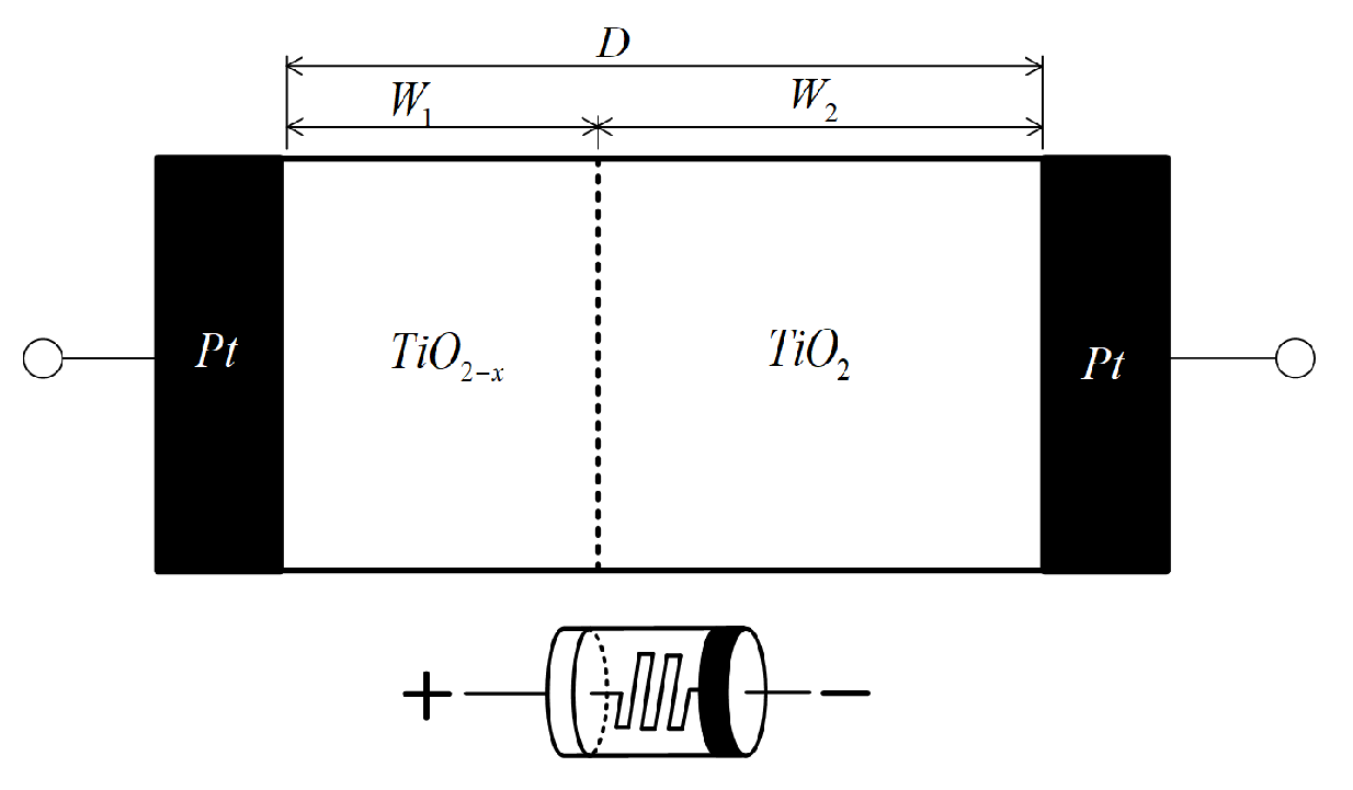
2. Memristor Model
3. Memristor-Based Basic Logic Gate and D-Flip-Flop
3.1. Logical OR/NOR and AND/NAND Gates
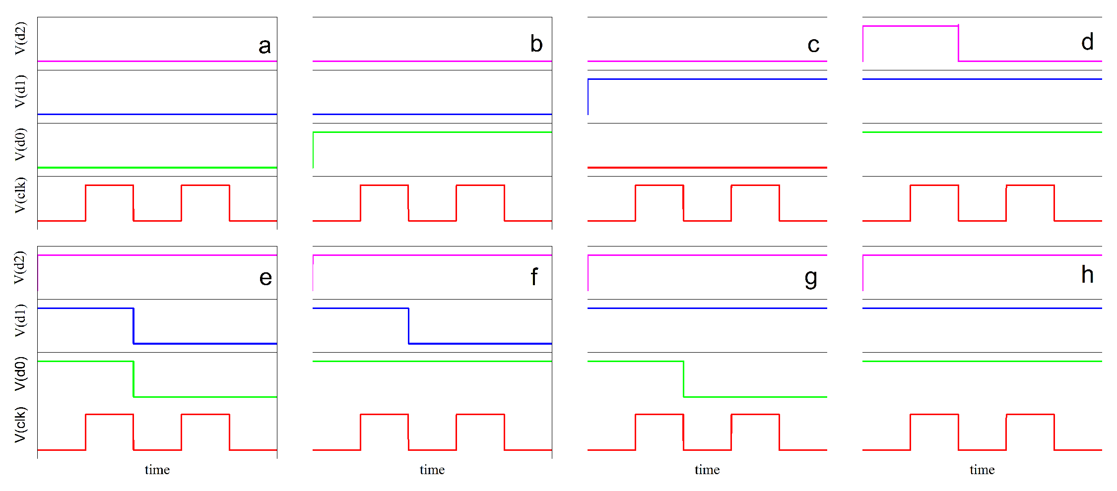
3.2. Memristor-Based Edge-Triggered D-Flip-Flop
4. Design of N-Bit Flash ADC
4.1. Traditional N-Bit Flash ADC
4.2. New 3-Bit Flash ADC
4.3. New 4-Bit Flash ADC
5. Conclusions
Author Contributions
Funding
Data Availability Statement
Conflicts of Interest
References
- Chua, L. Memristor-The missing circuit element. IEEE Trans. Circuit Theory 1971, 18, 507–519. [Google Scholar] [CrossRef]
- Strukov, D.B.; Snider, G.S.; Stewart, D.R.; Williams, R.S. The missing memristor found. Nature 2008, 453, 80–83. [Google Scholar] [CrossRef] [PubMed]
- Kvatinsky, S.; Wald, N.; Satat, G.; Kolodny, A.; Weiser, U.C.; Friedman, E.G. MRL—Memristor Ratioed Logic. In Proceedings of the 2012 13th International Workshop on Cellular Nanoscale Networks and Their Applications, Turin, Italy, 29–31 August 2012; pp. 1–6. [Google Scholar] [CrossRef]
- Robinett, W.; Pickett, M.; Borghetti, J.; Xia, Q.; Snider, G.S.; Medeiros-Ribeiro, G.; Williams, R.S. A memristor-based nonvolatile latch circuit. Nanotechnology 2010, 21, 235203. [Google Scholar] [CrossRef] [PubMed]
- Chang, T.; Jo, S.-H.; Kim, K.-H.; Sheridan, P.; Gaba, S.; Lu, W. Synaptic behaviors and modeling of a metal oxide memristive device. Appl. Phys. A 2011, 102, 857–863. [Google Scholar] [CrossRef]
- Kim, K.-H.; Gaba, S.; Wheeler, D.; Cruz-Albrecht, J.M.; Hussain, T.; Srinivasa, N.; Lu, W. A Functional Hybrid Memristor Crossbar-Array/CMOS System for Data Storage and Neuromorphic Applications. Nano Lett. 2012, 12, 389–395. [Google Scholar] [CrossRef] [PubMed]
- Zheng, N.; Mazumder, P. Learning in Memristor Crossbar-Based Spiking Neural Networks Through Modulation of Weight-Dependent Spike-Timing-Dependent Plasticity. IEEE Trans. Nanotechnol. 2018, 17, 520–532. [Google Scholar] [CrossRef]
- Bala, A.; Adeyemo, A.; Yang, X.; Jabir, A. High level abstraction of memristor model for neural network simulation. In Proceedings of the 2016 Sixth International Symposium on Embedded Computing and System Design (ISED), Patna, India, 15–17 December 2016; pp. 318–322. [Google Scholar] [CrossRef]
- Kim, Y.; SangHak, S.; Kyeong-Sik, M. Shared memristance restoring circuit for memristor-based Cellular Neural Networks. In Proceedings of the 2014 14th International Workshop on Cellular Nanoscale Networks and Their Applications (CNNA), Notre Dame, IN, USA, 29–31 July 2014; pp. 1–2. [Google Scholar] [CrossRef]
- Nguyen, T.V.; An, J.; Oh, S. Training, Programming, and Correction Techniques of Memristor-Crossbar Neural Networks with Non-Ideal Effects such as Defects, Variation, and Parasitic Resistance. In Proceedings of the 2021 IEEE 14th International Conference on ASIC (ASICON), Kunming, China, 26–29 October 2021; pp. 1–4. [Google Scholar] [CrossRef]
- Wang, N.; Li, B. Lagrange stability of complex-valued memristor-based neural networks. In Proceedings of the 2017 International Workshop on Complex Systems and Networks (IWCSN), Doha, Qatar, 8–10 December 2017; pp. 144–148. [Google Scholar] [CrossRef]
- Vourkas, I.; Sirakoulis, G.C. Emerging Memristor-Based Logic Circuit Design Approaches: A Review. IEEE Circuits Syst. Mag. 2016, 16, 15–30. [Google Scholar] [CrossRef]
- Jia, L.; Jiang, X.; Zhang, X.; Chi, M. Analysis and circuit implementation of a new fourth-order multi-wing chaotic system based on memristors. In Proceedings of the 2021 China Automation Congress (CAC), Beijing, China, 22–24 October 2021; pp. 5044–5049. [Google Scholar] [CrossRef]
- Minati, L.; Gambuzza, L.V.; Thio, W.J.; Sprott, J.C.; Frasca, M. A chaotic circuit based on a physical memristor. Chaos Solitons Fractals 2020, 138, 109990. [Google Scholar] [CrossRef]
- Yener, Ş.; Kuntman, H. A CMOS memristor implementation and its chaotic applications. In Proceedings of the 2012 20th Signal Processing and Communications Applications Conference (SIU), Mugla, Turkey, 18–20 April 2012; pp. 1–4. [Google Scholar] [CrossRef]
- Zidan, M.A.; Strachan, J.P.; Lu, W.D. The future of electronics based on memristive systems. Nat. Electron. 2018, 1, 22–29. [Google Scholar] [CrossRef]
- Luo, J.; Li, J.; Ning, N.; Liu, Y.; Yu, Q. The Effects of Comparator Dynamic Capacitor Mismatch in SAR ADC and Correction. IEEE Access 2018, 6, 7037–7043. [Google Scholar] [CrossRef]
- Palomo, B.; Muñoz, F.; Carvajal, R.G.; Garcia, J.R.; Marquez, F. An 8-bit 19MS/s low-power 0.35 μm CMOS pipelined ADC for DVB-H. Integration 2012, 45, 222–227. [Google Scholar] [CrossRef]
- Krishna, S.R.; Baghini, M.S.; Mukherjee, J. Current-mode CMOS pipelined ADC. In Proceedings of the IEEE EUROCON 2009, Saint Petersburg, Russia, 18–23 May 2009; pp. 205–210. [Google Scholar] [CrossRef]
- Bchir, M.; Hassen, N.; Ettaghzout, T.; Besbes, K. Low voltage low power current mode analog to digital converter flash. In Proceedings of the 2016 7th International Conference on Sciences of Electronics, Technologies of Information and Telecommunications (SETIT), Hammamet, Tunisia, 18–20 December 2016; pp. 553–556. [Google Scholar] [CrossRef]
- Huang, G.; Lin, P. A 1.0-V 6-b 40 MS/s time-domain flash ADC in 0.18 μm CMOS. Analog. Integr. Circuits Signal Process. 2013, 77, 285–289. [Google Scholar] [CrossRef]
- Huang, Y.; Chang, J.; Cheng, Y.; Chen, Z.; Hu, J.; Ji, X.; Li, F.; Li, J.; Li, Q.; Qian, X.; et al. The Flash ADC system and PMT waveform reconstruction for the Daya Bay experiment. Nucl. Instrum. Methods Phys. Res. Sect. A Accel. Spectrometers Detect. Assoc. Equip. 2018, 895, 48–55. [Google Scholar] [CrossRef]
- Ayesh, M.M.; Ibrahim, S.; Aboudina, M.M. A 15.5-mW 20-GSps 4-bit charge-steering flash ADC. In Proceedings of the 2015 IEEE 58th International Midwest Symposium on Circuits and Systems (MWSCAS), Fort Collins, CO, USA, 2–5 August 2015; pp. 1–4. [Google Scholar] [CrossRef]
- Prasad, J.M.R.; Kariyappa, D.B.S.; Holla, R. Design and Implementation of Flash ADC for Low Power Applications. IOSR J. VLSI Signal Process. 2014, 4, 41–46. [Google Scholar] [CrossRef]
- Maurya, A.; Rahi, P.; Koley, K.; Kumar, J. Implementation and Performance Analysis of Low Power 1 GHz 4-Bit Flash ADC Using III–V Tunnel-FET. Circuits Syst. Signal Process. 2023, 42, 1352–1368. [Google Scholar] [CrossRef]
- Bchir, M.; Hassen, N.; Besbes, K. A Novel High-Performance ADC Flash Based on Bulk-Driven Quasi-Floating Gate Current Mirror. In Proceedings of the 2020 17th International Multi-Conference on Systems, Signals & Devices (SSD), Sfax, Tunisia, 20–23 July 2020; pp. 780–785. [Google Scholar] [CrossRef]
- Yang, J.J.; Pickett, M.D.; Li, X.; Ohlberg, D.A.A.; Stewart, D.R.; Williams, R.S. Memristive switching mechanism for metal/oxide/metal nanodevices. Nat. Nanotechnol. 2008, 3, 429–433. [Google Scholar] [CrossRef] [PubMed]
- Yakopcic, C.; Taha, T.M.; Subramanyam, G.; Pino, R.E. Generalized Memristive Device SPICE Model and its Application in Circuit Design. IEEE Trans. Comput.-Aided Des. Integr. Circuits Syst. 2013, 32, 1201–1214. [Google Scholar] [CrossRef]


| CLK | D | Q |
|---|---|---|
| * | • | maintain |
| ↓ | 1 | 1 |
| 0 | 0 | |
| • | maintain |
| Input Analog Voltage | State of the Comparator Output | Output of ADC | ||||||||
|---|---|---|---|---|---|---|---|---|---|---|
| (0∼) | 0 | 0 | 0 | 0 | 0 | 0 | 0 | 0 | 0 | 0 |
| (∼) | 0 | 0 | 0 | 0 | 0 | 0 | 1 | 0 | 0 | 1 |
| (∼) | 0 | 0 | 0 | 0 | 0 | 1 | 1 | 0 | 1 | 0 |
| (∼) | 0 | 0 | 0 | 0 | 1 | 1 | 1 | 0 | 1 | 1 |
| (∼) | 0 | 0 | 0 | 1 | 1 | 1 | 1 | 1 | 0 | 0 |
| (∼) | 0 | 0 | 1 | 1 | 1 | 1 | 1 | 1 | 0 | 1 |
| (∼) | 0 | 1 | 1 | 1 | 1 | 1 | 1 | 1 | 1 | 0 |
| (∼1) | 1 | 1 | 1 | 1 | 1 | 1 | 1 | 1 | 1 | 1 |
| Item | Ref. [23] | Ref. [24] | Ref. [25] | Ref. [26] | This Work | This Work |
|---|---|---|---|---|---|---|
| Resolution (bits) | 4 | 4 | 4 | 4 | 3 | 4 |
| Technology | 65 nm | 90 nm | - | 0.18 nm | 50 nm | 50 nm |
| Input signal (V) | 0.6–0.9 | 0.1–1 | 0.1–1 | 0–0.8 | 0–1 | 0–1 |
| Voltage (V) | 1 | 1.8 | 1 | 0.8 | 1 | 1 |
| Delay (ns) | - | 100 | 11 | 0.16 | 17.8 | 70 |
| Power (mw) | 15.5 | 7.846 | 0.75 | 118.24 | 1.33 | 5.84 |
| Transistors | 180 | 165 | 82 | 266 | 36 | 62 |
| Memristors | 0 | 0 | 0 | 0 | 51 | 88 |
Disclaimer/Publisher’s Note: The statements, opinions and data contained in all publications are solely those of the individual author(s) and contributor(s) and not of MDPI and/or the editor(s). MDPI and/or the editor(s) disclaim responsibility for any injury to people or property resulting from any ideas, methods, instructions or products referred to in the content. |
© 2023 by the authors. Licensee MDPI, Basel, Switzerland. This article is an open access article distributed under the terms and conditions of the Creative Commons Attribution (CC BY) license (https://creativecommons.org/licenses/by/4.0/).
Share and Cite
Dai, G.; Du, X.; Xie, W.; Ni, T.; Han, M.; Wu, D. Circuit Design of 3- and 4-Bit Flash Analog-to-Digital Converters Based on Memristors. Electronics 2023, 12, 4069. https://doi.org/10.3390/electronics12194069
Dai G, Du X, Xie W, Ni T, Han M, Wu D. Circuit Design of 3- and 4-Bit Flash Analog-to-Digital Converters Based on Memristors. Electronics. 2023; 12(19):4069. https://doi.org/10.3390/electronics12194069
Chicago/Turabian StyleDai, Guangzhen, Xingyan Du, Wenxin Xie, Tianming Ni, Mingjun Han, and Daohua Wu. 2023. "Circuit Design of 3- and 4-Bit Flash Analog-to-Digital Converters Based on Memristors" Electronics 12, no. 19: 4069. https://doi.org/10.3390/electronics12194069
APA StyleDai, G., Du, X., Xie, W., Ni, T., Han, M., & Wu, D. (2023). Circuit Design of 3- and 4-Bit Flash Analog-to-Digital Converters Based on Memristors. Electronics, 12(19), 4069. https://doi.org/10.3390/electronics12194069