Abstract
This study focuses on the preparation of perovskite thin films using a simple set-up spin coating technique and the evaluation of their properties for application in switching memory devices. The properties of as-deposited films were thoroughly characterized using X-ray diffraction (XRD), field emission scanning electron microscopy (FESEM), UV-Vis spectroscopy, and a vibrating sample magnetometer (VSM). The results obtained revealed that the as-deposited films have a polycrystalline cubic structure. The film surfaces were uniform and densely packed without any voids, cracks, or pinholes. In addition, irregularly shaped grains were observed having an average size of , , , and for , , , and films, respectively. VSM analysis demonstrated that film exhibited superior magnetic properties compared to the other films. Furthermore, memory devices with structures were fabricated, and their I-V characteristics were measured. In order to assess their performance, an endurance test was conducted. The findings indicated that device exhibited higher ratio (), low Set/Reset voltages, lower power consumption (), and stable endurance with no significant degradation was observed in the LRS and HRS after 20 sweep cycles. These favorable parameters can be attributed to the reduced thickness, larger grain size, and excellent magnetic properties of the active-layer . Moreover, the conduction mechanism of the fabricated devices was investigated, revealing that the conduction in the LRS is primarily dominated by Ohmic behavior, while the HRS exhibited different conduction mechanisms.
1. Introduction
Resistive random access memory (RRAM) was introduced as a new data storage device and gained a lot of attention due to its small size, fast processing, high storage capacity, low power consumption, superior scalability, and rapid switching speed [1,2,3,4]. These remarkable characteristics make RRAM a promising alternative to Si-based flash memory, offering potential solutions to meet the increasing demands for enhanced data storage and more efficient memory technologies. RRAM consists of a metal-insulator-metal (MIM) structure where the resistance can be switched between a low resistance state (LRS) and a high resistance state (HRS) by applying an externally biased voltage [5,6]. This behavior, known as resistive switching (RS) or memristive, is a fundamental physical phenomenon that forms the basis for the ability of RRAM to store information [7].
Transition metal-perovskite oxides have emerged as highly promising active-layer materials for RRAM applications [8,9,10,11,12,13,14,15,16,17]. Nevertheless, the investigation of the RS behavior in specific materials such as , , , and has been relatively limited. In fact, the existing studies on these materials have shown remarkable RS properties, highlighting their potential for RRAM applications. For example, Schmitt et al. [18] found that amorphous films exhibited memristive behavior, showcasing consistent resistive switching and fast switching times, indicating their potential for efficient information storage and processing. Maity et al. [19] successfully fabricated a resistive switching device using a thin film prepared through pulsed laser deposition (PLD), displaying remarkable cyclic stability and a narrow operational voltage window. Moreover, Wan Jing et al. [7] investigated the RS behavior of PLD-fabricated thin films, revealing unipolar switching behavior with a high resistance ratio and excellent endurance and retention characteristics. Additionally, T Kim et al. [20] showed that the fabricated RRAM devices exhibited reset-first RS behavior and gradual resistance changes under AC pulse application, making them suitable for low-power synaptic devices in neuromorphic computing.
Herein, we synthesized perovskite thin films as switching materials to construct RRAMDs devices. The films were deposited on FTO substrates using a simple set-up spin coating method.
Spin coating is a widely used and highly effective technique for depositing thin films. One of the key advantages of this technique is its simplicity, which makes it a popular choice in laboratory settings [21]. It involves depositing a liquid precursor solution onto a substrate and then spinning the substrate at high speeds to produce a thin film with uniform thickness. The resulting films are of high quality and exhibit excellent surface coverage, which makes them ideal for a wide range of applications [21]. However, one of the disadvantages of spin coating is its cost. The equipment required for spin coating can be expensive, which makes it challenging for some researchers to adopt this technique. For this, we use simple and cost-effective setups to perform spin coating and prepare our films. This simple device involves spinning the substrate using a DC motor. The substrate was fixed to the holder by putting it on top of the motor.
In this study, we conducted a comparative analysis of the memristive properties of devices. Indeed, the RS behavior is influenced by various factors, including the properties of the active layer. Therefore, we focused our research on studying and evaluating the properties of the as-deposited spin-coated thin films using X-ray diffraction (XRD), field emission scanning electron microscopy (FESEM), UV-vis spectroscopy, and vibrating-sample magnetometer (VSM). This comprehensive approach allows for a thorough understanding of the properties and potential applications of the thin films in switching memory device applications.
2. Experimental Procedure
2.1. Materials
The materials used in this study are (BDH Chemicals, London, UK), (Loba Chemie, Maharashtra, India), (Loba Chemie), (BDH chemicals), (Panreac Applichem, Darmstadt, Germany), pure citric acid () (Loba Chemie), polyvinyl alcohol (PVA), ethylene glycol, and ammonia (). They are analytical grade and are used without further purification.
2.2. Film Preparation
2.2.1. Substrate Preparation
The FTO substrates underwent a thorough cleaning process utilizing an ultrasonic bath. This involved immersing the substrates in liquid detergent, followed by sequential rinsing with deionized water, acetone, and isopropanol for a duration of 20 each. Finally, the substrates were air-dried in ambient conditions.
2.2.2. Sol-Gel Preparation
Four solutions were prepared using stoichiometric amounts of 0.005 mol , and various agents of transition metal salts, which are: 0.005 mol , 0.005 mol , 0.005 mol and 0.005 mol . Each salt was dissolved along with in a separate beaker by adding 30 mL of a mix-solvent consisting of deionized water and ethanol in a specific ratio (. The solutions were then mixed at room temperature using a magnetic stirrer for a duration of 10 min until clear solutions were obtained. Afterwards, 0.010 mol of citric acid, which serves as a chelating agent to prevent aggregation, was added to each solution. Subsequently, the solutions were continuously stirred for an additional 10 min. Furthermore, amount of polyvinyl alcohol solution and of ethylene glycol were added to each solution to lower the formation temperature [22,23,24] and facilitate the polymerization [25]. To achieve a desired pH value of approximately 9, a few drops of ammonia were added. Finally, the solutions were continuously stirred for a duration of 3 to ensure complete homogeneity.
2.2.3. Spin Coating Set-Up
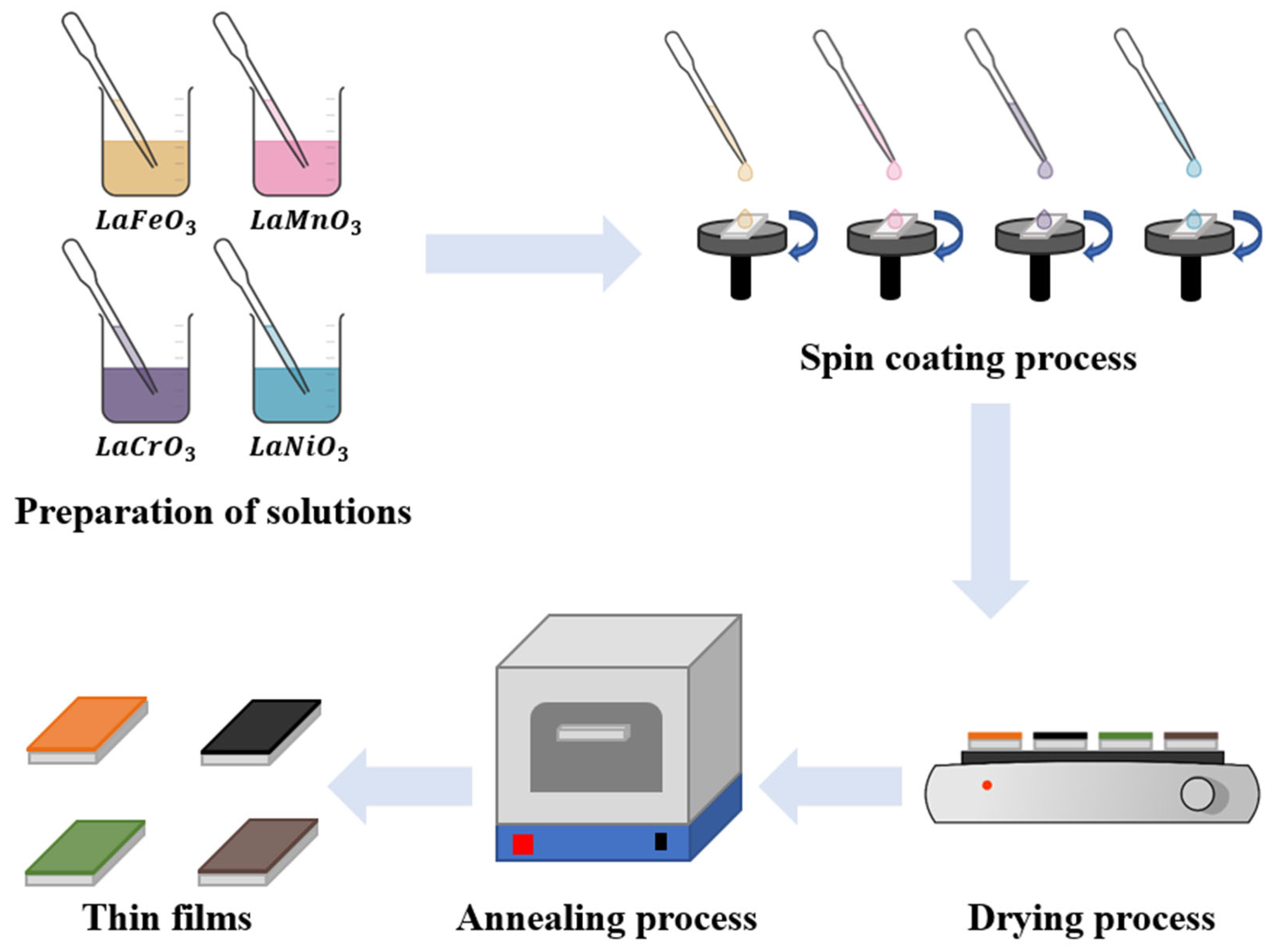
Figure 1 illustrates the setup of the spin coater used for synthesizing perovskite thin films. The setup incorporates a DC motor (DC 3–6 V, 1500 RPM) powered by 3 V batteries, operating at a consistent rotation speed of 1500 rpm. The substrate was fixed on a holder (spinning disk), which was placed on top of the motor. The substrate was securely held in place on the holder using double-sided tape during the spinning process. This method effectively prevented any potential shifting or movement of the substrate and ensured a uniform coating. The preparation procedure for the thin films using the spin coating technique is depicted in Figure 2. During the coating process, a small amount of the film material solution is dropped onto the center of the substrate. The motor is then turned on, and the substrate is rotated for 10 . The spinning motion generates centrifugal force, causing the solution to spread out evenly across the substrate, resulting in the formation of a thin film. The film was then dried on a hot plate for 10 min at to eliminate the solvents, and the process was repeated 10 times.

Figure 1.
Schematic diagram of self- made spin coater.
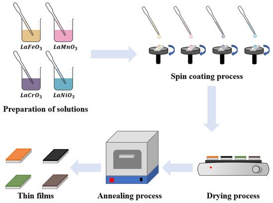
Figure 2.
Schematic diagram showing the preparation procedure of LaXO3 (X = Fe, Mn, Cr, Ni) thin films using spin coating technique.
2.3. Fabrication of Au/LaXO3 (M = Fe, Mn, Cr, Ni)\FTO Devices
The device is composed of a gold () top electrode, a active layer, and an bottom electrode substrate. A specialized shadow mask was used to deposit onto the synthesized films using a thermal deposition technique. The deposition of , with a thickness of , was carried out under high vacuum conditions to ensure accurate and controlled deposition of the layer. Figure 3a showcases a schematic picture of the memory device structure studied in this work, while Figure 3b shows the actual image of the fabricated devices.
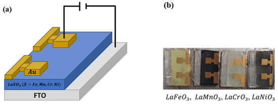
Figure 3.
(a) Schematic configuration of the Au/LaXO3 (X = Fe, Mn, Cr, Ni)/FTO memory device structure, and (b) Image of the actual fabricated resistive switching device.
2.4. Characterization Techniques
The thicknesses of the films were determined using contact profilometry (Dektak 150, Bruker, Billerica, MA, USA). The microstructural properties of the prepared films were measured at room temperature using a Rigaku Miniflex 600 X-ray diffractometer (, , , Tokyo, Japan) with a step size of and a scan rate of . The morphologies of the film surfaces were examined by a FE-SEM (JEOL JSM-7600F) using an accelerating voltage of . Absorbance and transmittance spectra measurements were conducted between and via a UV-vis spectrophotometer (Shimadzu UV-2600, Kyoto, Japan). Moreover, the resistive switching properties and the current-voltage (I-V) curves of the fabricated devices were measured at room temperature by a Keithley 2400-LV (Cleveland, OH, USA) source meter.
3. Results and Discussion
3.1. Microstructural Properties
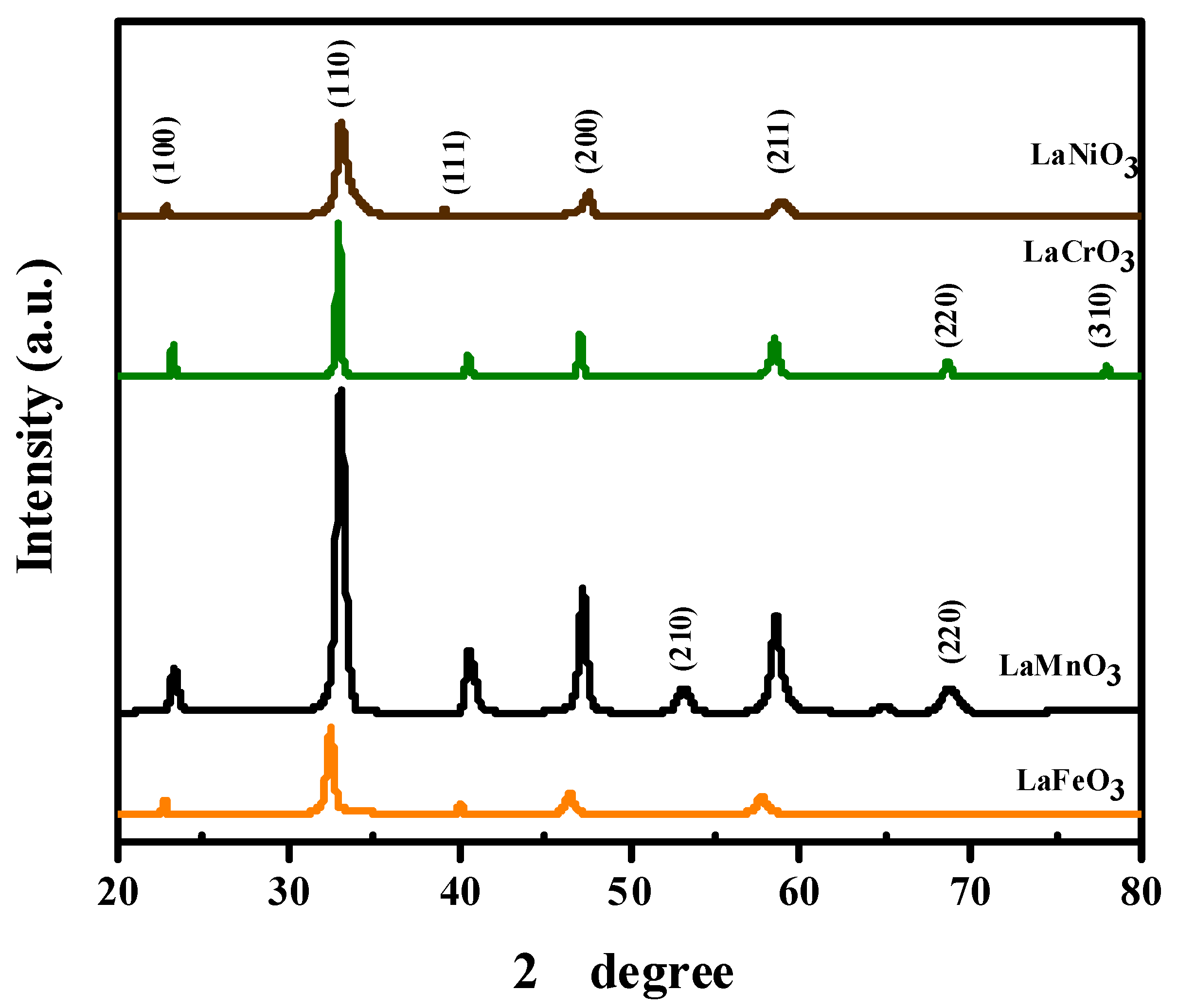
Figure 4 shows the spectra of the films deposited on substrates using the spin coating technique, carried out at room temperature. As can be observed, all the films are single-phase without any detectable impurities within the range studied. The characteristic peaks of the as-deposited films were indexed to the standard cards of (01-075-0439), (01-075-0440) (01-075-0441), and (00-033-0710), which correspond to the cubic structure with Pm-3m (221) space group. Furthermore, as seen in Figure 4, the peak intensity of sample was higher compared to the other samples, which could be attributed to it being the thickest sample (Table 1).

Figure 4.
XRD spectra of the as-deposited perovskite thin films.

Table 1.
The obtained structural parameters of the as-prepared thin films.
The following equations were used to compute the lattice parameter (a) and the cell volume for the cubic structure of the as-deposited thin films:
where and are miller indices and. is the interplanar spacing.
The calculation of the crystallite size (), micro-strain (, and dislocation density of the deposited films was conducted using the following equations [26]:
where, is the X-ray wavelength (), is the full width at half maximum (FWHM) of the maximum reflection measured in radians, and is the diffraction angle of the main peak.
The estimated values for the lattice parameters, cell volume, dislocation density, crystallite size, and micro-strain of the prepared films are listed in Table 1. The results obtained show that the lattice parameters and cell volume of the films were in good agreement with the matching card. Furthermore, we observed that as the crystallite size increased, the measured strain decreased. This is likely due to the decrease in grain boundary areas, which leads to a reduction in the number of defects in the film. Among the studied films, had the largest crystallite size and the smallest dislocation density, indicating a higher level of crystallinity.
3.2. Morphological Study
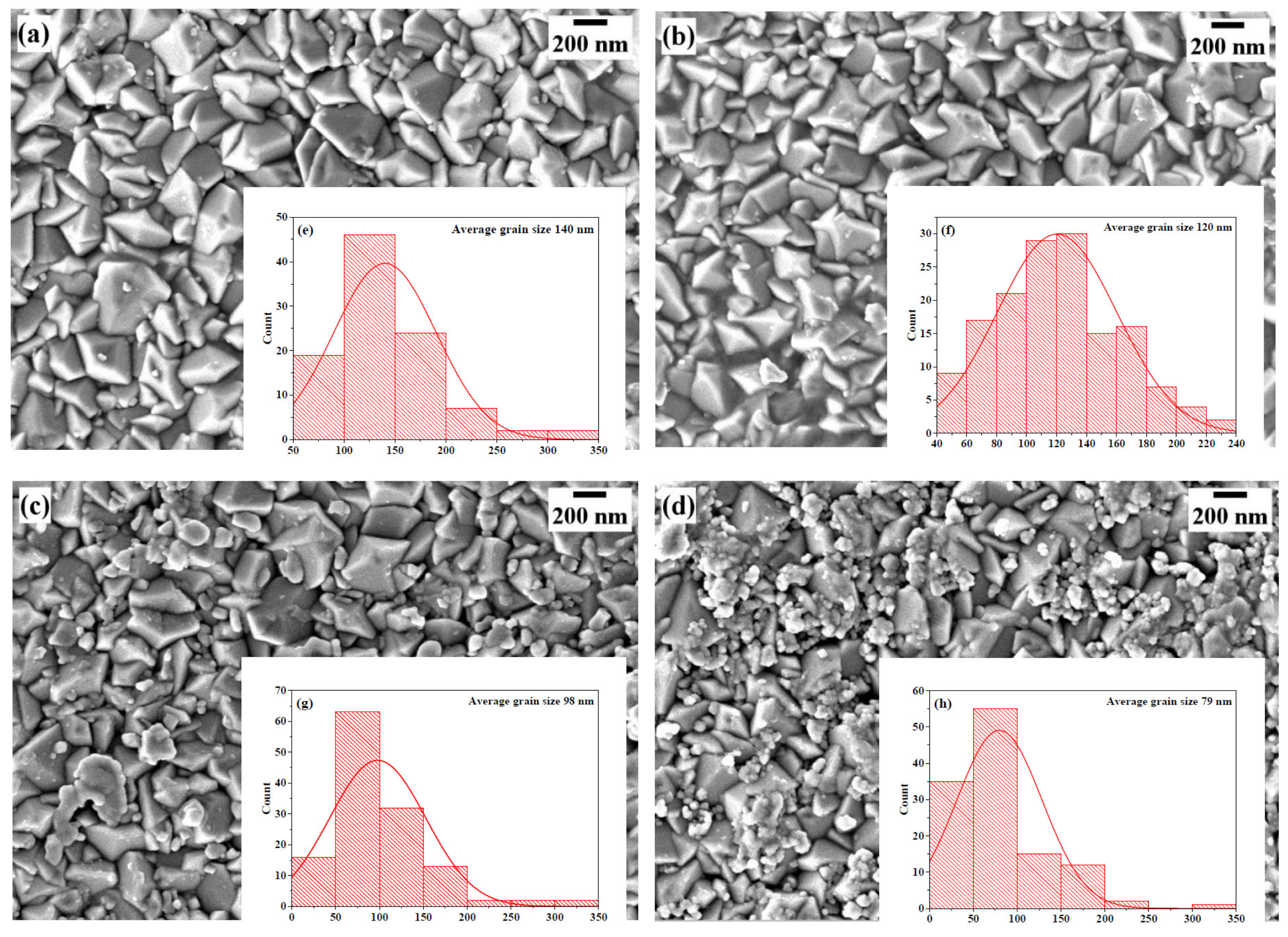
The surface morphologies of the LaXO3 (X = Fe, Mn, Cr, Ni) thin films were examined using FE-SEM. Figure 5 illustrates the micrographs of the prepared thin films, along with their respective grain size distribution histograms. Upon examination, the micrographs clearly showed the presence of irregularly shaped grains in the films with an average grain size of , , , and for , , , and films, respectively. We notice that the crystallite sizes calculated from XRD are smaller than the grain sizes measured by FESEM. This can be attributed to the fact that the grains are composed of multiple crystallites. Furthermore, all the film surfaces exhibit a uniform, homogeneous, and nearly densely packed surface morphology without the presence of any voids, cracks, or pinholes, indicating the high quality of the films. Notably, the film displayed a lower tendency for particle agglomeration, with minimal observed aggregation on its surface (Figure 5c). In contrast, the film exhibited a significant number of small particles that were observed to agglomerate (Figure 5d).

Figure 5.
FE-SEM images and particle size distribution histograms of (a) LaFeO3, (b) LaMnO3, (c) LaCrO3, and (d) LaNiO3 thin films with the corresponding grain size distribution (e–h), respectively.
3.3. Optical Properties
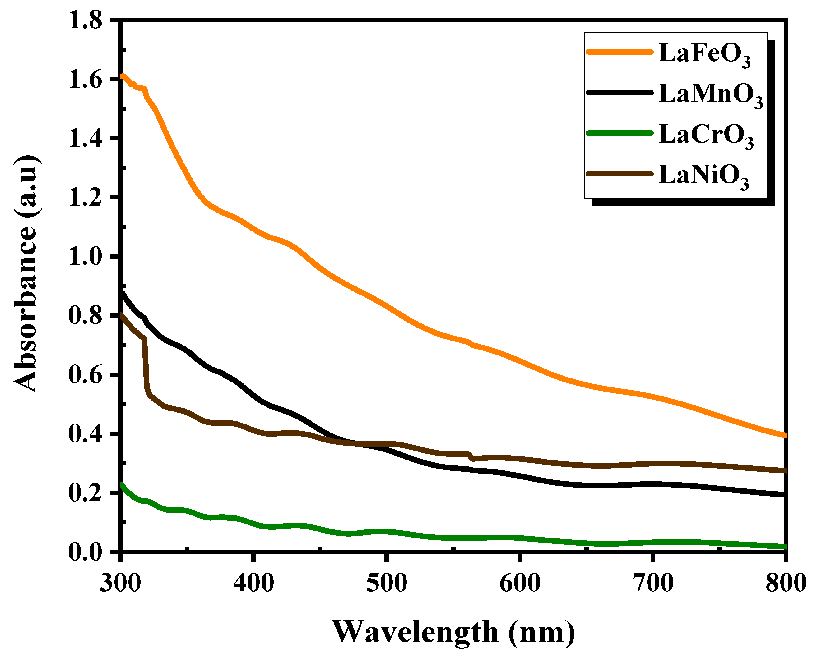
The optical absorbance of the as-prepared the as-prepared thin films was studied within the UV-visible region from 300 to 800 nm, as shown in Figure 6. The results revealed that all the fabricated films exhibited high absorption in the UV region, which decreased gradually with increasing wavelength. The film displayed a significantly higher absorbance compared to the other films. In fact, there are several parameters that can affect the film absorption, including crystal structure, film thickness, and surface morphology.

Figure 6.
Optical absorbance of LaXO3 (X = Fe, Mn, Cr, Ni) perovskite thin films.
The optical bandgaps of thin films were computed from the absorbance spectra using Tauc’s equation, which is given as follows:
where represents the absorption coefficient, is the photon energy, is a constant, and determines the type of transition. For direct transitions, , whereas for indirect transitions, [27]. The absorption coefficient was determined using the following relation:
Here is the thickness and is the absorbance of the film.
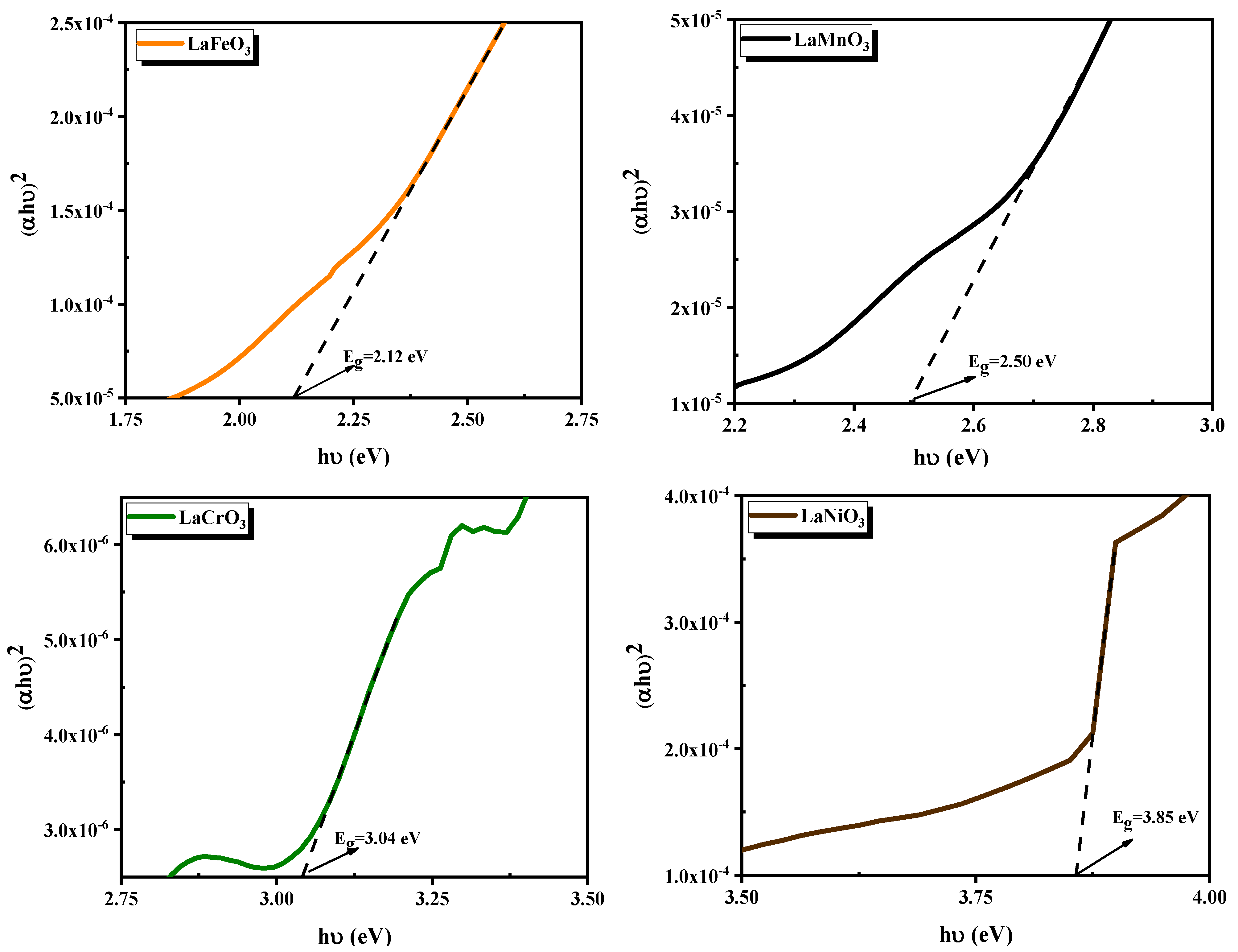
Figure 7 illustrates as a function of for the direct transitions of thin films. The was estimated by extrapolating the linear part of each curve onto the axis. and the obtained values are regrouped in Table 1. The band gap energies of and films are found to be , , , and , respectively. The measured band gap energies for and films align with the reported values ranging from 1.9 eV to 2.7 eV [28,29,30,31,32], 1.2 eV to 2.9 eV [29,31,33,34], 2.6 eV to 3.3 eV [27,29,31,35], and 2.2 eV to 3.8 eV [31,36], respectively.
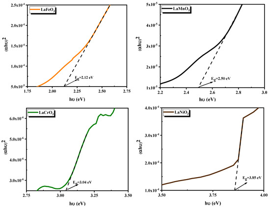
Figure 7.
(ahv)2 versus hv for direct transitions of the synthesized perovskite films.
3.4. Magnetic Properties
Figure 8 displays the hysteresis curves of magnetization (M) versus applied magnetic field (H) for thin films at room temperature, with H ranging from −10kOe to. +10kOe. The results indicate that all samples exhibit ferromagnetic behavior, with their corresponding , remanence , and coercivity values summarized in Table 2. Notably, film exhibits significantly higher magnetic properties compared to other samples. The higher magnetic properties of thin film can be attributed to the fact that the ions in have a high spin state, which leads to strong magnetic interactions between the ions and ions.
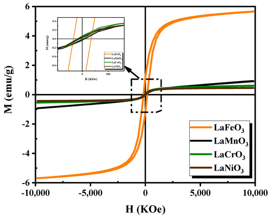
Figure 8.
Room-temperature magnetic hysteresis loops of the synthesized perovskite films.

Table 2.
Magnetic properties of the perovskite thin films.
Nevertheless, a weak ferromagnetic behavior observed in , , and films is attributed to the fact that lanthanum is unable to completely cancel out all the magnetization caused by the dipoles of , , and atoms [37]. Indeed, the magnetic properties can be influenced by several factors, including size, sample shape, crystallinity, synthesis method, magnetization direction, and annealing temperature [38].
3.5. I-V Characteristics
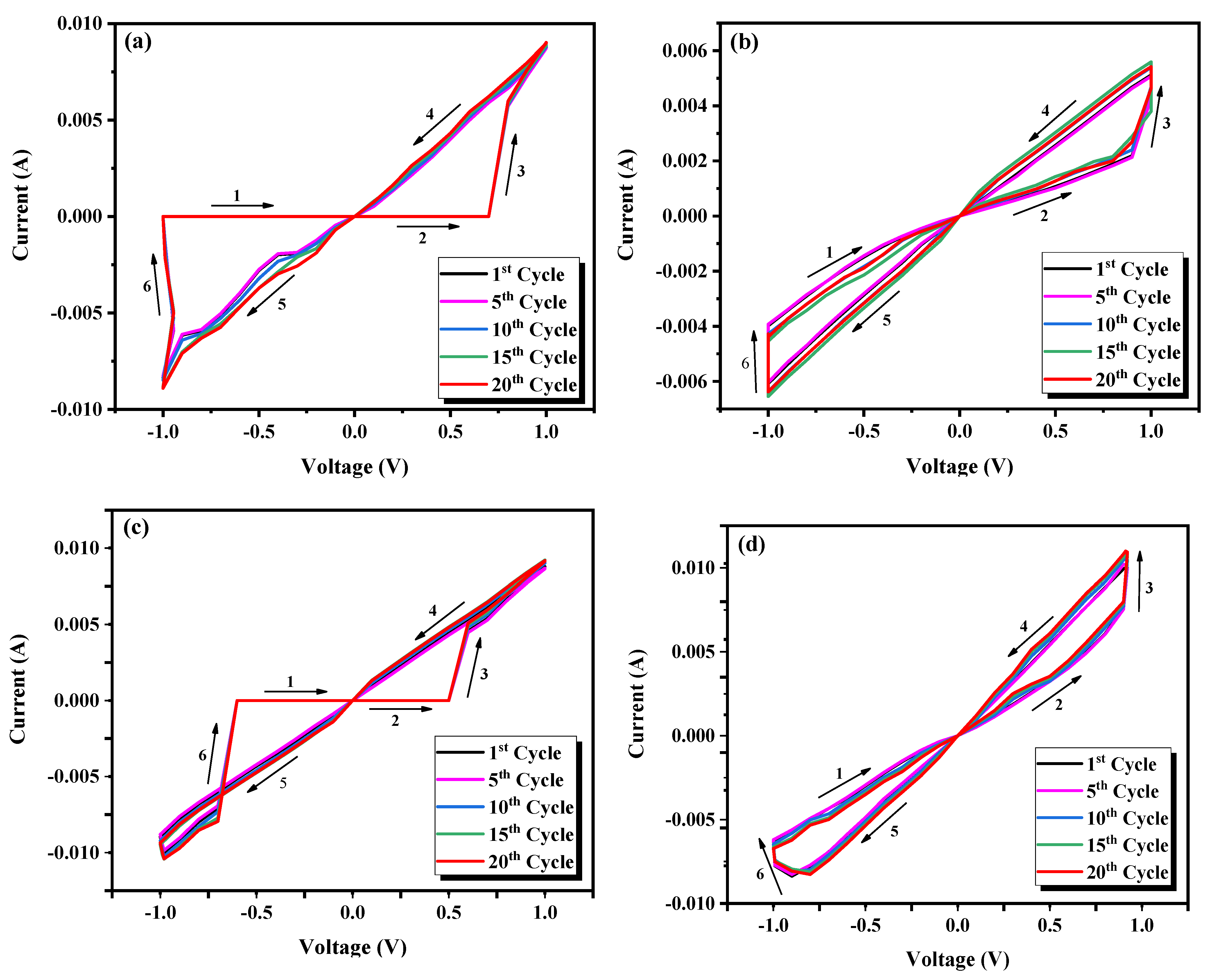
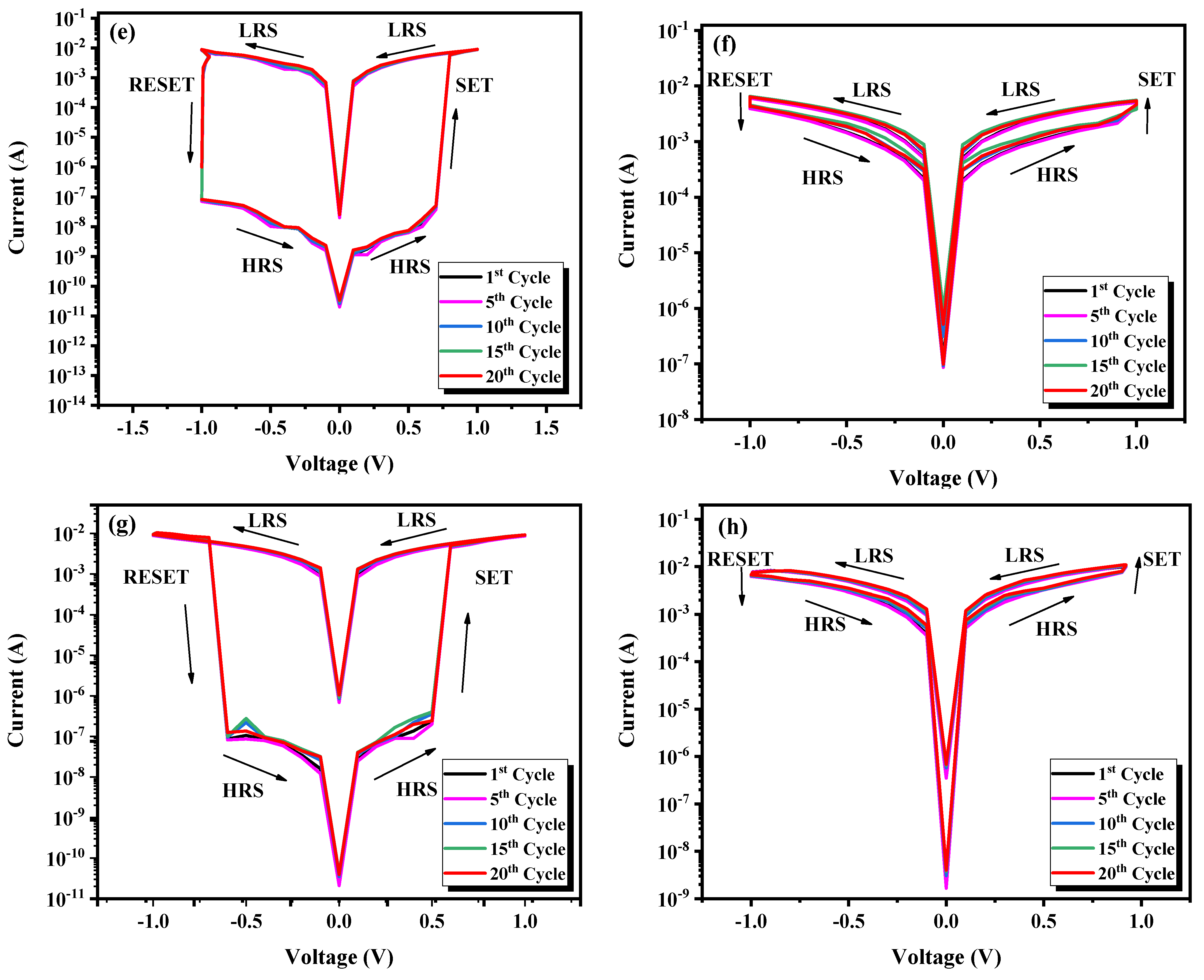
To characterize the electrical performance of the devices, the I-V characteristics were measured. Prior to conducting I-V measurements, it is necessary to perform an electroforming process in order to establish a strong electric field and initiate a controlled breakdown of the switching layer within the device. This process leads to the introduction of numerous oxygen vacancies into the active layer, which subsequently forms nanoscale conductive filaments. Thus, to prevent the device from being permanently damaged, the applied voltage is gradually increased while keeping the current below [39]. The I-V characteristics of the devices were measured during a DC voltage sweep of and the obtained curves are depicted in Figure 9a–d. As shown, all memory devices exhibit uniform bipolar RS behaviors. Furthermore, the I-V data are plotted on a semilogarithmic scale to clearly study the RS behavior of the device, as depicted in Figure 9e–h. The fabricated devices are initially in their HRS when the voltage sweeps from to . When the voltage sweeps from to , they switch from a HRS to a LRS in positive voltage. This transition results in a nonvolatile “ON” state, known as the “Set” process. Subsequently, the devices revert to a HRS from a LRS after the voltage sweeps from to and then returns from to , realizing the “OFF” state. This reverse transition is referred to as the “reset” process and is defined by the negative voltage.
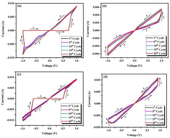
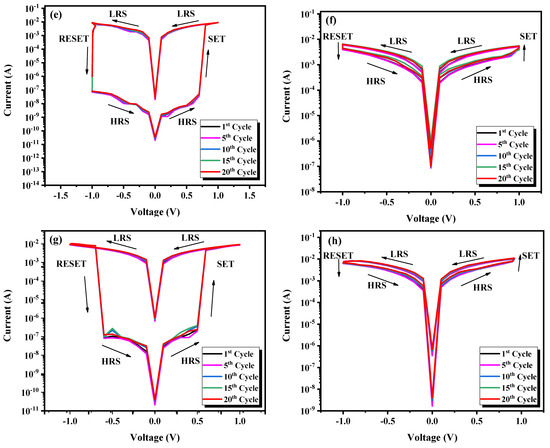
Figure 9.
Typical I-V characteristics of the prepared devices for (a) LaFeO3, (b) LaMnO3, (c) LaCrO3, and (d) LaNiO3. Characteristic I-V Curve of the devices with current in log scale for (e) LaFeO3, (f) LaMnO3, (g) LaCrO3, and (h) LaNiO3.
The switching parameters, which are: Set () and Reset () voltages, ratio, and power consumption for all fabricated devices, were calculated and depicted in Table 3. The ratio, defined as the ratio between the current values measured at a reading voltage of 0.2 V in and in states. The higher resistance ratio means a higher ON/OFF current ratio, leading to faster reading, fewer errors, and less power consumption [40]. Moreover, the power consumption was calculated by multiplying the reading voltage (0.2 V) and LRS current values. It is noteworthy to mention that reducing the power consumption of memory devices is directly related to minimizing the Set/Reset voltage [40]. Additionally, RRAM devices require a ratio greater than 10 to reduce the burden on the peripheral amplifier and simplify the amplifier circuit [40].

Table 3.
Switching parameters of the fabricated devices.
Based on the RS properties of the fabricated devices presented in Table 3, we can clearly notice that device exhibits the highest ratio, low Set/Reset voltages and the lowest power consumption. In fact, several parameters, including the properties of the active layer, can affect the RS properties. Previous studies have shown that as-deposited films with lower crystallinity demonstrated a higher resistance ratio [41], while films deposited at higher substrate temperatures exhibited excellent bipolar resistive switching behavior attributed to their larger grain size and higher crystallinity [42]. Moreover, the uniformity and density of the surface play a role in achieving non-volatile, reliable, reproducible, and long-term stable resistive switching [43]. Additionally, a decrease in the set/reset operating voltage was observed with a decrease in the thickness of the nanodisk [44]. In our study, the remarkable RS properties of device are likely due to its higher magnetic properties, larger grain size, and lower thickness, making it a promising candidate for switching memory device applications.
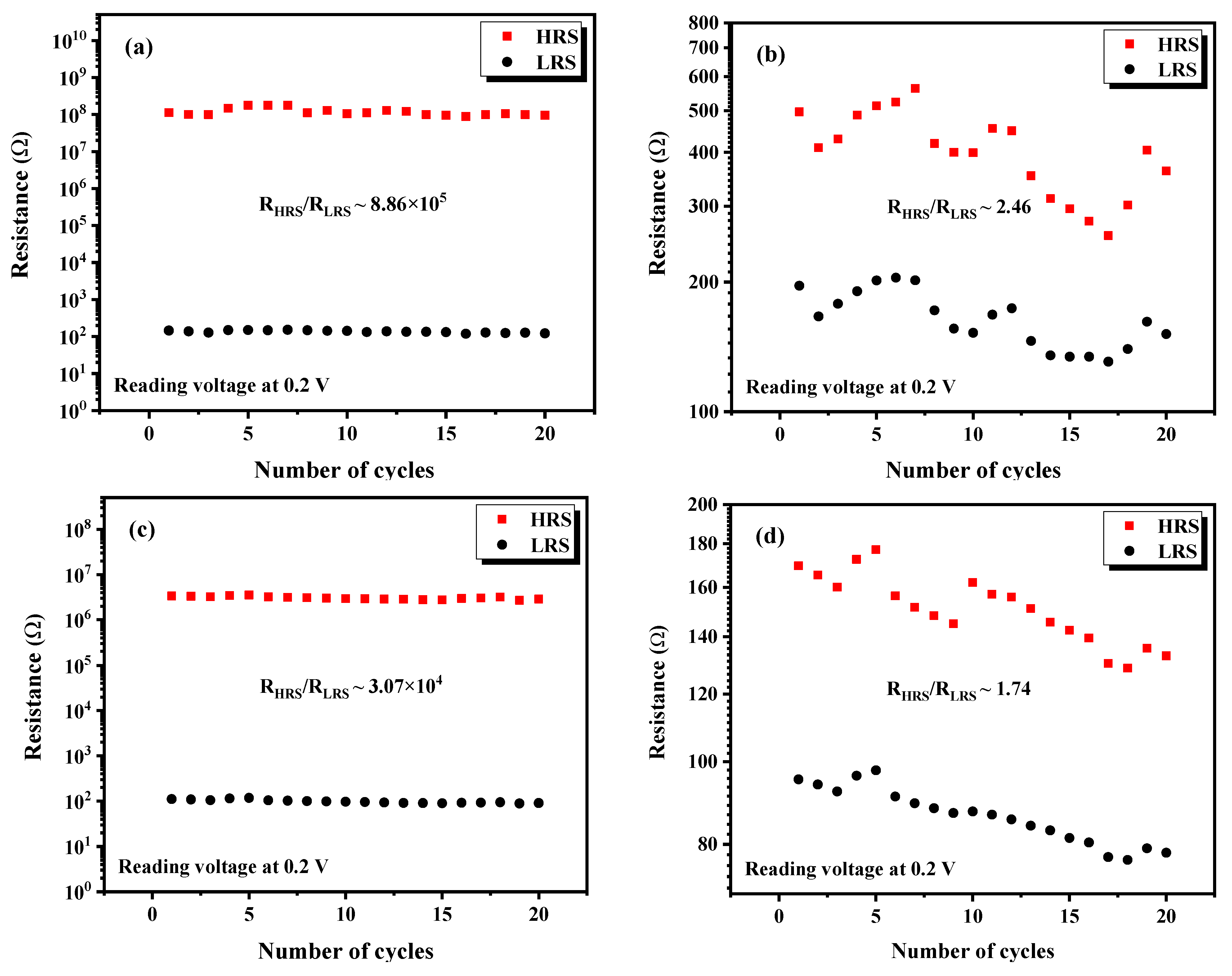
To evaluate the performance of the fabricated devices, an endurance test was conducted. Figure 10 shows changes in resistance for the LRS and HRS states with a reading voltage of during 20 consecutive sweep cycles. Remarkably, the devices based on and displayed remarkable stability in switching between HRS and LRS throughout the 20 cycles, demonstrating reproducible read/write characteristics. Conversely, the devices based on and exhibit poor endurance characteristics with some fluctuations.
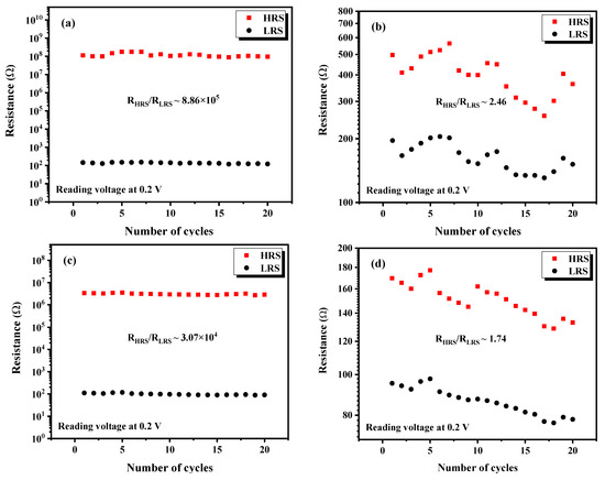
Figure 10.
Endurance characteristics of (a) LaFeO3, (b) LaMnO3, (c) LaCrO3, and (d) LaNiO3 devices in the HRS and LRS recorded over 20 cycles.
Table 4 provides a comparative overview of the switching parameters (, , and ) of various transition metal perovskite oxide devices reported in previous studies, along with the results obtained from our fabricated devices. It is noteworthy that the HRS/LRS ratio of in our study reached surpasses the values reported in the previous studies listed in Table 4.

Table 4.
Switching parameters of different devices from previous studies.
To gain a deeper insight into the bipolar RS behavior observed in the devices, further analysis was performed to determine their conduction mechanisms. The conduction mechanisms in both the LRS and HRS were thoroughly investigated to provide clarity on the overall conduction behavior exhibited by these devices. In general, three common conduction mechanisms are used to fit the nonlinear relationship of the I-V curve: Schottky emission, trap-controlled space charge-limited conduction (SCLC), and Poole-Frenkel emission [17]. The SCLC model includes three sections distinguished by the slope of : (i) for Ohm’s region, (ii) for the Child’s law region or trap-unfilled SCLC region, and (iii) for steep regions or trap-filled SCLC region [39,50]. Poole-Frenkel emission can be confirmed by curve fitting [50,51], whereas the fitting of function is widely adopted to verify Schottky emission [50,51].
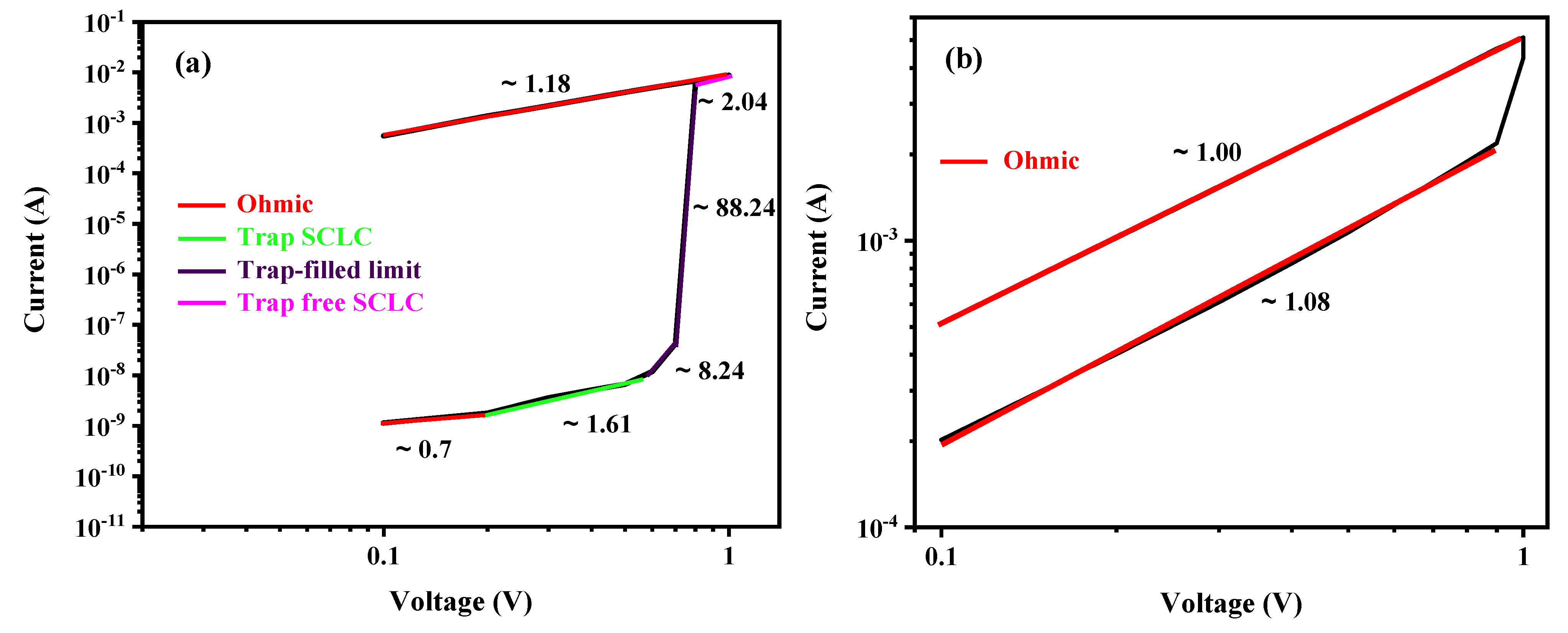
To further investigate and understand the mechanism, double logarithmic graphs of the obtained electrical linear curves of the positive bias region were developed, as shown in Figure 11. Fittings were performed for both LRS and HRS in different voltage regimes, and the straight lines indicate the fitting results. As can be clearly seen from Figure 11, the I-V curves of LRS exhibit a linear relationship for all the fabricated devices with a slope of and for (Figure 11a), (Figure 11b), (Figure 11c), and (Figure 11d), respectively, which indicates the Ohmic conduction behavior. This result can be assigned to the formation of conductive filaments (CFs) by the accumulation of defects, such as oxygen vacancies (), in the thin film during the set process [7,39,52]. Nevertheless, in the HRS region for device, the current depends linearly on the voltage with a slope of , exhibiting an Ohmic current conduction behavior (Figure 11b). The I-V curve of device divides into two regions. In the low voltage range from to , the current depends linearly on the voltage with a slope of , showing the Ohmic conduction (Figure 11d). Nevertheless, at higher voltages, nonlinear behavior is observed. The nonlinear conduction mechanisms, such as Schottky emission, Poole–Frenkel emission, and SCLC, were employed to model the nonlinearity observed in the I-V curves. It was found that the Schottky emission mechanism provides the best fit for the data and occurs as a result of thermal excitation caused by an increase in the applied voltage. The inset curve in Figure 11d shows the linear dependence of versus . The injected carriers are then able to surpass the Schottky barrier at the electrode/active layer interface and traverse through the active layer at higher voltages in the HRS [7,50,51]. However, in the HRS region for and active layers, the I-V curves were more complicated and could be divided into four different conduction regions according to the subsequent increase in applied voltage, which are ohmic, trap-filling space-charge-limited current (SCLC), trap-filled limit (TFL), and trap-free SCLC [53,54]. At a low applied bias voltage, the slope of each curve was calculated and found to be approximately and for and , respectively. The slopes are nearly equal to 1, indicating that the Ohmic conduction behavior was dominant due to the thermally generated charge carriers exceeding the injected carriers and contributing to the conduction at the interface between the electrode and the active layer. Indeed, the generated carriers depend on film properties and the applied voltage. In the Ohmic region, the charge carriers do not traverse the entire film due to the carrier transit time being greater than the dielectric relaxation time of the material [46,55,56]. As the magnitude of the applied voltage bias increased, the slope of the curves exhibited a corresponding increase, reaching values of and for and , respectively. Thus, the SCLC dominates over the Ohmic behavior, in accordance with Child’s square law (). Therefore, the number of free charge carriers injected from the electrode into the active layer increased, surpassing the thermally generated charge carriers. This led to the formation of space charges near the electrode/active layer interface. However, these charges encounter difficulties in further movement through the material. Consequently, a region of SCLC is formed in the vicinity of the electrodes and extends throughout the active layer, effectively limiting the further movement of charges. It is important to note that most of the injected charge here does not contribute to the current, and a portion of it occupies the traps [53,56].
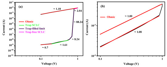
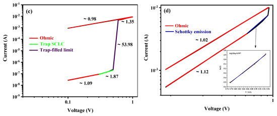
Figure 11.
I-V Curves in double logarithmic scale for LRS and HRS with fitted conduction mechanism in positive bias region for (a) LaFeO3, (b) LaMnO3, (c) LaCrO3, and (d) LaNiO3.
After applying a higher voltage, a significant increase in current is observed around and for and , respectively. This abrupt change in current behavior can be attributed to the saturation of all traps by the injected charge carriers, resulting in a steep slope increase from approximately two to infinity (). This phenomenon is associated with the formation of filaments and the filling up of all-trap sites. In this state, the injected charge carriers are able to move freely across the active layer thickness, leading to a rapid change in current and ultimately bringing it to the LRS [36,46,49]. Thus, trap-controlled SCLC conduction mechanisms become dominant in these devices.
Finally, beyond this transition region, a distinct behavior is observed for and . For , a region with a slope of is observed. In this region, all traps are completely filled, and they no longer have any effect on charge injection. As a result, any injected charge fully contributes to the current, following an ideal trap-free square law (). This behavior has been reported in previous studies [45,49]. On the other hand, for , a different region is observed, characterized by a slope of , indicating an Ohmic conduction by the linear relationship between the applied voltage and the resulting current.
4. Conclusions
In summary, perovskite thin films have been successfully prepared on the FTO substrates via a simple set-up spin coating technique, and their properties were thoroughly investigated for potential application in switching memory devices. The as-deposited films were found to have a polycrystalline cubic structure with uniform and densely packed surfaces. The devices demonstrated a bipolar RS behavior at room temperature. Notably, the device exhibited higher ratio, low Set/Reset voltages, lower power consumption, and stable endurance with no significant degradation observed in the LRS and HRS after 20 sweeps, suggesting its potential for switching memory device applications. Furthermore, a study of the conduction mechanism in the fabricated devices revealed that the LRS exhibited primarily Ohmic behavior, whereas the HRS demonstrated different conduction mechanisms. However, further investigations are needed to measure the retention time and to improve on the ratio of the fabricated memory devices.
Author Contributions
Conceptualization, A.L.; methodology, R.K.A. and A.M.A.; validation, R.K.A.; formal analysis, R.K.A.; investigation, R.K.A.; data curation, R.K.A.; writing—original draft preparation, R.K.A.; writing—review and editing, A.L.; visualization, R.K.A.; supervision, A.L. All authors have read and agreed to the published version of the manuscript.
Funding
This research was funded by Deanship of Scientific Research, Qassim University, Saudi Arabia, grant number [COS-2022-1-3-J-31574]. And The APC was funded by [Qassim University, represented by the Deanship of Scientific Research].
Data Availability Statement
The data used to support the findings of this research are included in this paper.
Acknowledgments
The authors gratefully acknowledge Qassim University, represented by the Deanship of Scientific Research, for the financial support for this research under the number (COS-2022-1-3-J-31574) during the academic year 1444 AH/2022 AD.
Conflicts of Interest
The authors declare no conflict of interest.
References
- Akinaga, H.; Shima, H. Resistive Random Access Memory (ReRAM) Based on Metal Oxides. Proc. IEEE 2010, 98, 2237–2251. [Google Scholar] [CrossRef]
- Pan, F.; Gao, S.; Chen, C.; Song, C.; Zeng, F. Recent Progress in Resistive Random Access Memories: Materials, Switching Mechanisms, and Performance. Mater. Sci. Eng. R Rep. 2014, 83, 1–59. [Google Scholar] [CrossRef]
- Waser, R.; Dittmann, R.; Staikov, G.; Szot, K. Redox-based Resistive Switching Memories–Nanoionic Mechanisms, Prospects, and Challenges. Adv. Mater. 2009, 21, 2632–2663. [Google Scholar] [CrossRef]
- Shang, D.-S.; Sun, J.-R.; Shen, B.-G.; Matthias, W. Resistance Switching in Oxides with Inhomogeneous Conductivity. Chin. Phys. B 2013, 22, 067202. [Google Scholar] [CrossRef]
- Asif, M.; Kumar, A. Resistive Switching in Emerging Materials and Their Characteristics for Neuromorphic Computing. Mater. Today Electron. 2022, 1, 100004. [Google Scholar] [CrossRef]
- Fatheema, J.; Shahid, T.; Mohammad, M.A.; Islam, A.; Malik, F.; Akinwande, D.; Rizwan, S. A Comprehensive Investigation of MoO 3 Based Resistive Random Access Memory. RSC Adv. 2020, 10, 19337–19345. [Google Scholar] [CrossRef]
- Hu, W.-J.; Hu, L.; Wei, R.-H.; Tang, X.-W.; Song, W.-H.; Dai, J.-M.; Zhu, X.-B.; Sun, Y.-P. Nonvolatile Resistive Switching and Physical Mechanism in LaCrO3 Thin Films. Chin. Phys. Lett. 2018, 35, 047301. [Google Scholar] [CrossRef]
- Yan, Z.; Guo, Y.; Zhang, G.; Liu, J. High-performance Programmable Memory Devices Based on Co-doped BaTiO3. Adv. Mater. 2011, 23, 1351–1355. [Google Scholar] [CrossRef]
- Liu, D.; Wang, N.; Wang, G.; Shao, Z.; Zhu, X.; Zhang, C.; Cheng, H. Nonvolatile Bipolar Resistive Switching in Amorphous Sr-Doped LaMnO3 Thin Films Deposited by Radio Frequency Magnetron Sputtering. Appl. Phys. Lett. 2013, 102, 134105. [Google Scholar] [CrossRef]
- Acharya, S.K.; Nallagatla, R.V.; Togibasa, O.; Lee, B.W.; Liu, C.; Jung, C.U.; Park, B.H.; Park, J.-Y.; Cho, Y.; Kim, D.-W. Epitaxial Brownmillerite Oxide Thin Films for Reliable Switching Memory. ACS Appl. Mater. Interfaces 2016, 8, 7902–7911. [Google Scholar] [CrossRef] [PubMed]
- Seong, T.-G.; Bum Choi, K.; Seo, I.-T.; Oh, J.-H.; Won Moon, J.; Hong, K.; Nahm, S. Resistive Switching Properties of Amorphous Pr0.7Ca0.3MnO3 Films Grown on Indium Tin Oxide/Glass Substrate Using Pulsed Laser Deposition Method. Appl. Phys. Lett. 2012, 100, 212111. [Google Scholar] [CrossRef]
- Deng, H.; Zhang, M.; Li, T.; Wei, J.; Chu, S.; Du, M.; Yan, H. Nonvolatile Unipolar Resistive Switching Behavior of Amorphous BiFeO3 Films. J. Alloys Compd. 2015, 639, 235–238. [Google Scholar] [CrossRef]
- Janousch, M.; Meijer, G.I.; Staub, U.; Delley, B.; Karg, S.F.; Andreasson, B.P. Role of Oxygen Vacancies in Cr-doped SrTiO3 for Resistance-change Memory. Adv. Mater. 2007, 19, 2232–2235. [Google Scholar] [CrossRef]
- Szot, K.; Speier, W.; Bihlmayer, G.; Waser, R. Switching the Electrical Resistance of Individual Dislocations in Single-Crystalline SrTiO3. Nat. Mater. 2006, 5, 312–320. [Google Scholar] [CrossRef]
- Fu, Y.J.; Xia, F.J.; Jia, Y.L.; Jia, C.J.; Li, J.Y.; Dai, X.H.; Fu, G.S.; Zhu, B.Y.; Liu, B.T. Bipolar Resistive Switching Behavior of La0.5Sr0.5CoO3−σ Films for Nonvolatile Memory Applications. Appl. Phys. Lett. 2014, 104, 223505. [Google Scholar] [CrossRef]
- Ranieri, M.G.A.; Ortega, P.P.; Moreno, H.; Ramirez, M.A.; Aguiar, E.C.; Simoes, A.Z. Resistive Switching and Multiferroic Behavior of La0.5Pr0.5FeO3 Ferrite Thin Films. J. Alloys Compd. 2021, 851, 156936. [Google Scholar] [CrossRef]
- Cheng, C.-R.; Tsai, M.-H.; Hsu, T.-H.; Li, M.-J.; Huang, C.-L. Resistive Switching Characteristics and Mechanism of Lanthanum Yttrium Oxide (LaYO3) Films Deposited by RF Sputtering for RRAM Applications. J. Alloys Compd. 2023, 930, 167487. [Google Scholar] [CrossRef]
- Schmitt, R.; Kubicek, M.; Sediva, E.; Trassin, M.; Weber, M.C.; Rossi, A.; Hutter, H.; Kreisel, J.; Fiebig, M.; Rupp, J.L.M. Accelerated Ionic Motion in Amorphous Memristor Oxides for Nonvolatile Memories and Neuromorphic Computing. Adv. Funct. Mater. 2019, 29, 1804782. [Google Scholar] [CrossRef]
- Maity, I.; Mukherjee, A.K.; Thakur, A.D. Enhanced Stability and Low Operational Voltage of Resistive Switching Behavior in Defect Engineered LaMnO3 Film. Appl. Phys. A 2023, 129, 11. [Google Scholar] [CrossRef]
- Kim, D.; Lee, J.; Kim, J.; Sohn, H. Reset-First and Multibit-Level Resistive-Switching Behavior of Lanthanum Nickel Oxide (LaNiO3−x) Thin Films. Materials 2023, 16, 4992. [Google Scholar] [CrossRef] [PubMed]
- Orava, J.; Kohoutek, T.; Wagner, T. Deposition Techniques for Chalcogenide Thin Films. In Chalcogenide Glasses; Elsevier: Amsterdam, The Netherlands, 2014; pp. 265–309. [Google Scholar]
- Shimizu, Y.; Murata, T. Sol–Gel Synthesis of Perovskite-type Lanthanum Manganite Thin Films and Fine Powders Using Metal Acetylacetonate and Poly (Vinyl Alcohol). J. Am. Ceram. Soc. 1997, 80, 2702–2704. [Google Scholar] [CrossRef]
- Feng, J.; Liu, T.; Xu, Y.; Zhao, J.; He, Y. Effects of PVA Content on the Synthesis of LaFeO3 via Sol–Gel Route. Ceram. Int. 2011, 37, 1203–1207. [Google Scholar] [CrossRef]
- Dung, N.X. Synthesis of Nanometric LaCr0.5Mn0.5O3 Perovskite at Low Temperature by the Polyvinyl Alcohol Gel Combustion Method. J. Exp. Nanosci. 2015, 10, 511–519. [Google Scholar] [CrossRef]
- Liu, X.; Ji, H.; Gu, Y.; Xu, M. Preparation and Acetone Sensitive Characteristics of Nano-LaFeO3 Semiconductor Thin Films by Polymerization Complex Method. Mater. Sci. Eng. B 2006, 133, 98–101. [Google Scholar] [CrossRef]
- Williamson, G.K.; Hall, W.H. X-Ray Line Broadening from Filed Aluminium and Wolfram. Acta Metall. 1953, 1, 22–31. [Google Scholar] [CrossRef]
- Polat, O.; Durmus, Z.; Coskun, F.M.; Coskun, M.; Turut, A. Engineering the Band Gap of LaCrO3 Doping with Transition Metals (Co, Pd, and Ir). J. Mater. Sci. 2018, 53, 3544–3556. [Google Scholar] [CrossRef]
- Luu, C.L.; Van Nguyen, T.T.; Nguyen, T.; Nguyen, P.A.; Hoang, T.C.; Ha, C.A. Thin Film Nano-Photocatalyts with Low Band Gap Energy for Gas Phase Degradation of p-Xylene: TiO2 Doped Cr, UiO66-NH2 and LaBO3 (B = Fe, Mn, and Co). Adv. Nat. Sci. Nanosci. Nanotechnol. 2018, 9, 015003. [Google Scholar] [CrossRef]
- Aljurays, R.; Loucif, A.; Amer, M.; Al-Mayouf, A.M. Preparation and Characterization of Lanthanum-Based Perovskite Oxides LaMO3 (M=Fe, Cr, Mn) Thin Films by Electrophoretic Deposition. Mater. Res. Express 2023, 10, 065902. [Google Scholar] [CrossRef]
- Scafetta, M.D.; Cordi, A.M.; Rondinelli, J.M.; May, S.J. Band Structure and Optical Transitions in LaFeO3: Theory and Experiment. J. Phys. Condens. Matter 2014, 26, 505502. [Google Scholar] [CrossRef]
- Pan, G.T.; Chong, S.; Pan, K.L.; Chang, M.B.; Yang, T.C.K.; Shukla, P. The Study of Photoelectrochemical Properties of LaMnO3, LaFeO3, LaCrO3, and LaNiO3 Photoelectrodes for Hydrogen Production. Clean Technol. Env. Policy 2017, 19, 1557–1565. [Google Scholar] [CrossRef]
- Sun, X.; Tiwari, D.; Fermin, D.J. Promoting Active Electronic States in LaFeO3Thin-Films Photocathodes via Alkaline-Earth Metal Substitution. ACS Appl. Mater. Interfaces 2020, 12, 31486–31495. [Google Scholar] [CrossRef] [PubMed]
- Mahapatra, A.; Mahapatra, S.; Sahu, R.; Kumar, P. Preparation and Optical Characterization of LaMnO3 Thin Films by Sol–Gel Technique. In Processing and Characterization of Materials; Springer: Berlin/Heidelberg, Germany, 2021; pp. 157–164. [Google Scholar]
- Gharbi, B.; Boukhachem, A.; Amlouk, M.; Oueslati, M.; Dkhil, B.; Meftah, A. Physical Investigations on LaMn1−xNixO3 Perovskite Sprayed Thin Films along with Surface Magnetic Applications. Appl. Phys. A 2020, 126, 604. [Google Scholar] [CrossRef]
- Koli, P.B.; Kapadnis, K.H.; Deshpande, U.G.; Tupe, U.J.; Shinde, S.G.; Ingale, R.S. Fabrication of Thin Film Sensors by Spin Coating Using Sol-Gel LaCrO3 Perovskite Material Modified with Transition Metals for Sensing Environmental Pollutants, Greenhouse Gases and Relative Humidity. Environ. Chall. 2021, 3, 100043. [Google Scholar] [CrossRef]
- Omari, E.; Makhloufi, S.; Omari, M. Preparation by Sol–Gel Method and Characterization of Co-Doped LaNiO3 Perovskite. J. Inorg. Organomet. Polym. Mater. 2017, 27, 1466–1472. [Google Scholar] [CrossRef]
- Shah, A.A.; Ahmad, S.; Azam, A. Investigation of Structural, Optical, Dielectric and Magnetic Properties of LaNiO3 and LaNi1−XMxO3 (M=Fe, Cr & Co; X=5%) Nanoparticles. J. Magn. Magn. Mater. 2020, 494, 165812. [Google Scholar]
- Çoban Özkan, D.; Türk, A.; Celik, E. Synthesis and Characterizations of Sol–Gel Derived LaFeO3 Perovskite Powders. J. Mater. Sci. Mater. Electron. 2020, 31, 22789–22809. [Google Scholar] [CrossRef]
- Shariffar, A.; Salman, H.; Siddique, T.A.; Gebril, W.; Manasreh, M.O. Resistive Switching in FTO/CuO–Cu2O/Au Memory Devices. Micro Nano Lett. 2020, 15, 853–857. [Google Scholar] [CrossRef]
- Di, J.; Du, J.; Lin, Z.; Liu, S.; Ouyang, J.; Chang, J. Recent Advances in Resistive Random Access Memory Based on Lead Halide Perovskite. InfoMat 2021, 3, 293–315. [Google Scholar] [CrossRef]
- Dao, T.B.T.; Pham, K.N.; Cheng, Y.-L.; Kim, S.S.; Phan, B.T. Correlation between Crystallinity and Resistive Switching Behavior of Sputtered WO3 Thin Films. Curr. Appl. Phys. 2014, 14, 1707–1712. [Google Scholar] [CrossRef]
- Du, Q.; Wang, W.; Li, S.; Zhang, D.; Zheng, W. Effects of Substrate Temperature on the Structural, Optical and Resistive Switching Properties of HfO2 Films. Thin Solid. Film. 2016, 608, 21–25. [Google Scholar] [CrossRef]
- Ke, W.; Yang, X.; Liu, T. Resistance Switching Effect of Memory Device Based on All-Inorganic Cspbbri2 Perovskite. Materials 2021, 14, 6629. [Google Scholar] [CrossRef] [PubMed]
- Ahn, Y.; Son, J.Y. Thickness-Dependent Resistive Switching Memory Characteristics of NiO Nanodisks Fabricated by AAO Nanotemplate. Curr. Appl. Phys. 2023, 54, 44–48. [Google Scholar] [CrossRef]
- Gao, C.; Zhang, P.; Zhang, C.; Dong, C.; Jiang, C.; Liu, Q.; Xue, D. Multiferroic and Multilevel Resistive Switching Properties of LaFeO3–PbTiO3 Films Grown on Nb: SrTiO3 (001) Substrate. Ceram. Int. 2015, 41, S851–S855. [Google Scholar] [CrossRef]
- Shringi, A.K.; Betal, A.; Sahu, S.; Saliba, M.; Kumar, M. Resistive Switching and Synaptic Behavior of Perovskite Lanthanum Orthoferrite Thin Film for Neuromorphic Computing. IEEE Trans. Electron. Devices 2022, 69, 6465–6470. [Google Scholar] [CrossRef]
- Li, J.; Wu, L.; Ma, M.; Song, R.; Dong, C.; Wei, J.; Li, J.; Wang, X.; Li, M. Effect of Annealing Temperature on Resistive Switching Behavior of Al/La0.7Sr0.3MnO3/LaNiO3 Devices. Curr. Appl. Phys. 2023, 46, 21–26. [Google Scholar] [CrossRef]
- Liu, D.-Q.; Cheng, H.-F.; Wang, G.; Zhu, X.; Shao, Z.-Z.; Wang, N.-N.; Zhang, C.-Y. Memristive Properties of Transparent (La, Sr)MnO3 Thin Films Deposited on ITO Glass at Room Temperature. IEEE Electron. Device Lett. 2013, 34, 1506–1508. [Google Scholar] [CrossRef]
- Xu, Z.; Jin, K.; Gu, L.; Jin, Y.; Ge, C.; Wang, C.; Guo, H.; Lu, H.; Zhao, R.; Yang, G. Evidence for a Crucial Role Played by Oxygen Vacancies in LaMnO3 Resistive Switching Memories. Small 2012, 8, 1279–1284. [Google Scholar] [CrossRef]
- Zheng, R.; Wu, L.; Li, J.; Wang, X.; Li, M.; Wei, J.; Li, J. Electro-Optical Modulation on Resistive Switching Behavior in Ag/BaTiO3/LaNiO3 Device. Mater. Lett. 2021, 293, 129658. [Google Scholar] [CrossRef]
- Lim, E.W.; Ismail, R. Conduction Mechanism of Valence Change Resistive Switching Memory: A Survey. Electronics 2015, 4, 586–613. [Google Scholar] [CrossRef]
- Wang, L.-Q.; Li, W.-H.; Tang, X.-G.; Guo, X.-B.; Liu, Q.-X.; Jiang, Y.-P.; Tang, Z.-H. Bipolar Resistive Switching Characteristics of PbZrO3/LaNiO3 Heterostructure Thin Films Prepared by a Sol–Gel Process. Ceram. Int. 2021, 47, 5617–5623. [Google Scholar] [CrossRef]
- Niittymäki, M.; Lahti, K.; Suhonen, T.; Metsäjoki, J. DC Conduction and Breakdown Behavior of Thermally Sprayed Ceramic Coatings. IEEE Trans. Dielectr. Electr. Insul. 2017, 24, 499–510. [Google Scholar] [CrossRef]
- Kwan, C.P.; Street, M.; Mahmood, A.; Echtenkamp, W.; Randle, M.; He, K.; Nathawat, J.; Arabchigavkani, N.; Barut, B.; Yin, S. Space-Charge Limited Conduction in Epitaxial Chromia Films Grown on Elemental and Oxide-Based Metallic Substrates. AIP Adv. 2019, 9, 055018. [Google Scholar] [CrossRef]
- Chiu, F.-C. A Review on Conduction Mechanisms in Dielectric Films. Adv. Mater. Sci. Eng. 2014, 2014, 578168. [Google Scholar] [CrossRef]
- Gupta, G.; Banerjee, S.; Dutta, S.; Aarnink, A.A.I.; Schmitz, J.; Kovalgin, A.Y.; Hueting, R.J.E. Charge Carrier Transport and Electroluminescence in Atomic Layer Deposited Poly-GaN/c-Si Heterojunction Diodes. J. Appl. Phys. 2018, 124, 084503. [Google Scholar] [CrossRef]
Disclaimer/Publisher’s Note: The statements, opinions and data contained in all publications are solely those of the individual author(s) and contributor(s) and not of MDPI and/or the editor(s). MDPI and/or the editor(s) disclaim responsibility for any injury to people or property resulting from any ideas, methods, instructions or products referred to in the content. |
© 2023 by the authors. Licensee MDPI, Basel, Switzerland. This article is an open access article distributed under the terms and conditions of the Creative Commons Attribution (CC BY) license (https://creativecommons.org/licenses/by/4.0/).


