Abstract
Dual-Core Lockstep (DCLS) is one of the most commonly used techniques in applications requiring functional safety. As the semiconductor process nodes keep shrinking, the DCLS technique is also more and more frequently seen in industrial or even consumer electronics. The paper presents the novel approach to the DCLS technique. While the typical approach is to set the slave core delay as a fixed number of clock cycles, we allow the checker core to run freely behind the main core within the constrained boundaries of clock cycles. This increases the temporal diversity needed for common mode failure mitigation. The system integrity provided by DCLS may also be used in the area of security applications. In this paper, we show that the proposed Variable Delayed Dual-Core Lockstep technique can flatten the power consumption correlation between the running cores, essential for a wide range of attacks. The proposed technique was implemented in the RISC-V processor core and verified in the Xilinx VCU108 FPGA platform.
1. Introduction
The continuous process of feature size shrinking follows the demand for more functionalities embedded in the same chip. However, the negative effect and the consequence of the growing complexity of modern Systems-on-Chip (SoCs) is the increasing susceptibility to soft errors caused by radiation and interference []. The design and implementation techniques once used solely to satisfy the reliability standards and safety mechanisms, such as those specified in ECSS-E-ST-70C for space applications [] or ISO26262 for automotive domain [], are more commonly used in the industrial electronics or even consumer market.
One of the widely known techniques for error detection in microprocessor systems is the checkpoint-oriented method that allows rollback recovery after detecting error [,]. It is a purely software method that checks the program flow using calculated signatures. The drawback of this method is that the signature is checked periodically, leaving the system unprotected between two checkpoints. The dual-core lockstep [] is an error detection technique based on hardware redundancy. Two instances of processor cores (i.e., central processing unit, CPU) execute exactly the same program allowing the error checker to detect any differences in the primary outputs. Generally, double the resources are needed for DCLS implementation in exchange for almost immediate error detection. On the other hand, the recovery from error mode is not trivial. It can rely on the checkpointing mentioned earlier, use additional recovery hardware or, as in most cases, require a complete system reset for resynchronization. To overcome this disadvantage, the TCLS (Triple-Core Lockstep) was introduced []. This approach adds a third redundant processor core; therefore, the faulty device may be identified based on majority voter. As a result, the correct architectural state can be immediately restored. Quick resynchronization is the major advantage of the TCLS technique, but the big resource overhead limits its use for safety-critical application.
The DCLS technique presents a widely acknowledged balance between error detection and recovery capabilities and resource utilization. This makes it one of the most commonly adopted error detection techniques in the industry. The paper presents the novel approach to the DCLS implementation. While the typical approach is to set the slave core delay as a fixed number of clock cycles, we allow the checker core to run freely behind the main core within the constrained boundaries of clock cycles. This increases the temporal diversity needed for common mode failure (CMF) mitigation. In this paper, we show that the proposed Variable Delayed Dual-Core Lockstep (VDCLS) technique can also flatten the power consumption correlation between running cores. The introduced power disruption caused by variable delay between processing cores makes it more difficult for an attacker to infer about the executed code and inject precisely timed faults. The proposed technique was implemented in the RISC-V [] processor core and verified in the Xilinx VCU108 FPGA platform.
The paper is organized as follows. Section 2 presents the related work and background for the conducted research. Section 3 describes the process of enhancing the regular multicore processor core with the VDCLS technique. The simulation and FPGA results are gathered in Section 4. Section 5 shows brief VDCLS failure analysis. The paper ends with a conclusion.
2. Related Work
The lockstepping technique can be applied at different levels of the computer system. The redundant logic, called the Sphere of Replication (SoR), may be located at system level, sub-system level or CPU level []. The system level means replication of the whole CPU system including main memories, while the sub-system level excludes main memories as they are typically protected anyway with other EDAC (Error Detection and Correction) means. These types of lockstepping systems are popular in servers and mainframes [,]. The CPU-level lockstepping has been also widely adopted by the industry. The availability of Commercial Off-The-Shelf (COTS) DCLS products include, for example, STMicroelectronics SPC574K72/SPC57EM80 [] or NXP MPC5643L [], both based on the e200zx core []. Another example is Texas Instruments TMS570LC4357 HerculesTM [], based on the ARM Cortex-R5 []. There is also a wide range of intellectual property products (IP cores) immediately available on the market, such as ARM Cortex-M33 [] or the Synopsys ARC® Functional Safety Processor IP line []. More interestingly, UltraSoC released an IP that is claimed to be able to turn any regular processor core into a lockstepping one [].
Before any technique is adopted by the industry, it must undergo a research phase. Indeed, the CPU-level dual core lockstep technique is still a subject of scientific research. There are many papers describing the process of enhancing the already existing cores with the DCLS technique. The authors of [] exploit the well-established 16-bit openMSP430 architecture. In [], the authors use the Xilinx MicroBlaze soft processor core. The ARM Cortex-A9 processor embedded into Zynq-7000 Xilinx device is used in []. There is also a growing number of papers concerning the rapidly emerging RISC-V architecture []. As stated before, the DCLS technique requires the resources of two CPUs, cancelling the multicore performance gain and increasing power consumption. To mitigate this, the authors of [] proposed an on-demand core synchronization with additional post-processing. Adaptive lockstep architecture using Cobham Gaisler’s LEON3 processor is presented in []. Other research is devoted to the problem accompanying the DCLS technique, that is error state recovery and rollback to the safe state [,]. A very interesting concept is also described in []. This article proposes a heterogeneous architecture that explores the DCLS technique using two different processing units: a hard-core Arm Cortex-A9 and a soft-core RISC-V-based processor.
The above brief description of the research on CPU-level dual-core lockstep architectures shows that, apart from the specific features, the most generic DCLS architecture presented in Figure 1 is used. The master and slave cores are identical. Slave core (CPU1) inputs are delayed by the constant number of clock cycles, whereas master core (CPU0) outputs have to be delayed by the same number of clock cycles to feed the output checker for comparison. One of the reasons behind the development of VDCLS technique is the fact that the most of the modern DCLS processors offer the lock/split feature [] that allows user to decide if processor should work as a regular dual-core multicore processor or in lockstep mode. In such a case, to work in the classic lockstep mode, the slave core has to be disconnected from the system bus and cache memories and fed with master core data to stay in synchronization. The novelty in the present work is based on the fact that we decided to maintain all the master and slave connections to most of system busses and keep cores synchronized by implementing additional logic. The design process of the proposed solution along with its consequences and results is presented in the following sections.
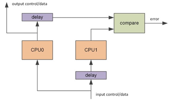
Figure 1.
Block diagram of a typical dual-core lockstep processor.
3. Design Architecture
The proposed Variable Delayed Dual-Core Lockstep (VDCLS) technique is implemented using the CCRV32ST processor core [,,] utilizing the RISC-V standard “GC” instruction set. The CCRV32ST integer pipeline is depicted in Figure 2. Its main features are:
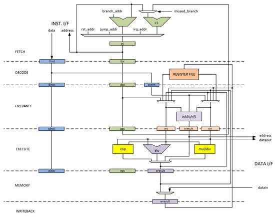
Figure 2.
Integer unit datapath of the CCRV32ST processor core.
- RV32GCX instruction set;
- Six-stage integer pipeline;
- Single-issue, in-order design;
- Gshare branch prediction;
- Single or multicore implementation;
- Up to 1.38 DMIPS/MHz/Core;
- Up to 2.10 CoreMark/MHz/Core;
- Custom instruction set extension;
- On-chip debug support.
The adopted processor is suitable for use in application-specific integrated circuits (ASIC) and in the field-programmable gate array devices (FPGA). The latter is commonly used as a design and verification framework due to its re-programmability feature. The main idea of the implementation process was to use the already existing CCRV32ST multicore infrastructure including the instruction and data caches and bus interconnects. Consequently, one of the design aims, i.e., to implement the lock/split feature mentioned earlier, was easily achievable. The block diagram of the typical processor implementation is presented in Figure 3. The following subsections briefly describe the VDCLS design phases.
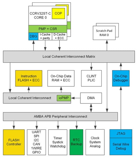
Figure 3.
Block diagram of a typical CCRV32ST processor system-on-chip.
3.1. Checker Module
The first step during the VDCLS implementation was to develop the Checker Module (Figure 4). The Checker Module receives the main outputs from the master and slave cores, optionally calculates output signature and buffers the results. The main core outputs consist of the current core program counter, executed instruction, instruction result and stored data. In the classic approach, when the slave core is delayed, e.g., by two clock cycles, the comparison is straightforward as it is made between the master core results and the slave core results delayed by a constant number of clock cycles. In the discussed case, the Checker Module constantly tracks the delay between the two cores and selects the appropriate slave core results for the comparison.
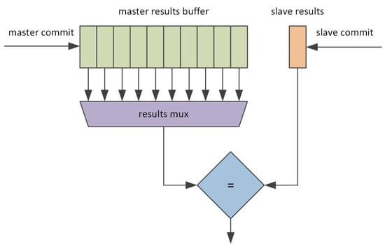
Figure 4.
Block diagram of the VDCLS Checker Module.
3.2. VDCLS Controller Module
The capacity of the Checker Module buffer is limited; moreover, the slave core cannot overtake the master core in the program execution. As the result, the program execution freedom by master and slave cores has to be constrained. The VDCLS Controller Module analyzes the current delay between two cores and injects stall cycles to the master core, when the slave core approaches the buffer limits, or to the slave core, to keep to slave core behind the master core (Figure 5). The necessity of injecting stall cycles is the main drawback of the proposed solution. However, the results shown in the later sections indicate that the impact of these additional cycles is negligible. The size of the Checker Module buffer constraints the stall injection thresholds. A bigger module reduces the need for stall cycles that impacts the processor performance.
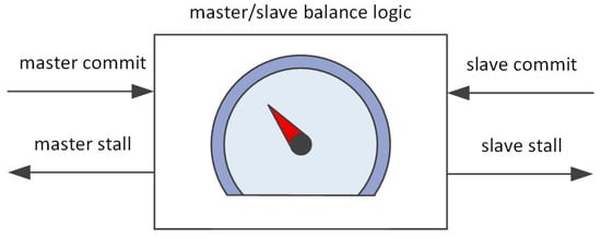
Figure 5.
VDCLS Controller Module simplified block diagram.
3.3. Cache Synchronization
In the described approach we decided to leave both master and slave cores connected independently to the main memory system busses. In comparison with classic DCLS implementation, this step increased the SoR area with the instruction and data cache memories. Each core fetches an instruction to its cache memories using separate requests on the system bus. This introduces additional protection against single point of failures (SPOF) resulting from the single data fetch that propagates to both cores. In general, in such a system, caches are protected using parity or Error Correction Codes (ECC), but this additional layer significantly hinders side channel manipulation. The attacker would need to intervene in two bus transactions taking place in two hard-to-predict time points. The same mechanism is used for data caches with one exception, that only the master core is capable of issuing store transactions to the system bus to update main memory or change peripherals state. Data caches are implemented as write-through with a write-no-allocate policy. This means that a cache miss during write does not require line refill. However, already allocated lines need updates in both master and slave cores. As the result, data dependency hazards such as read-after-write (RAW) can occur between cores during VDCLS execution. To resolve this issue, data caches were modified to mutually monitor their read and write attempts and if necessary postpone their action to prevent fetching incorrect data.
Figure 6 shows the exemplary situation when the master core performed write operation (W(B)) before the slave core could read the older value (R(B)). The system behavior in such a situation depends on whether the read value is in cache or has to be loaded from the main memory. After a cache hit, the slave core will use the value already existing in the cache memory. Otherwise, the bus transaction will occur causing a load of the incorrect value. To prevent such a situation, the master core is forced to wait for the slave core to finish the previous read operation. The importance of the cache transaction monitoring and synchronization mechanisms is shown in the Figure 7. It depicts the hypothetical situation when master and slave cores cause an entire system deadlock. The improperly implemented synchronization between both cores can lead to a situation when master and slave cores will indefinitely wait for each other to complete the operation. The implemented hardware mechanisms were extensively verified through PC simulation to ensure non-deadlock operation and maintain data coherency between master and slave cores. As a result, no external assistance from user software or compiler is needed. The VDCLS processor executes the same binary files as the original CCRV32ST processor core.
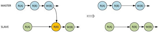
Figure 6.
Slave attempt to read data after master updated main memory.
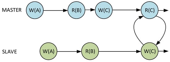
Figure 7.
Potential source of deadlock between master and slave cores.
3.4. Interrupt Injection
Just like the Checker Module, the interrupt module had to be modified to monitor the balance between the master and slave cores. Upon an incoming interrupt or exception event, the dedicated logic calculates the place in the slave interrupt buffer where the interrupt has to be injected (Figure 8). As the result, both cores see the interrupt in the same architectural state.
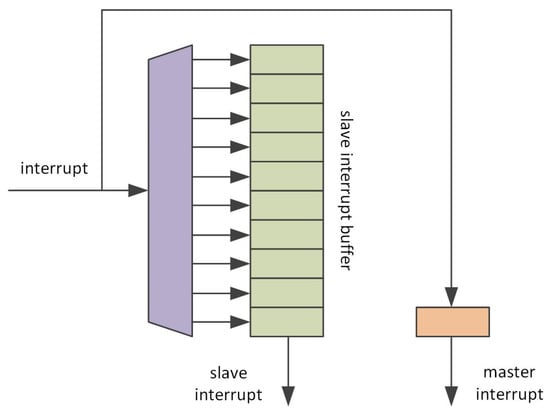
Figure 8.
Block diagram of the VDCLS Interrupt Injection Module.
3.5. Peripheral Bus
In general, the peripheral address space is non-idempotent. It means that read and write operations can have side effects. Moreover, a read operation can return a different value without an explicit write operation before (e.g., timers, counters, etc.). As the result, in contrast to the processor caches, only the master core is allowed to perform read and write operations. The dedicated module queues master read results and ensures that the slave core sees the correct read values.
4. Results
This section presents the results of the VDCLS technique implementation using the CCRV32ST processor core. Figure 9 presents the sample trace logged during the PC simulation of VDCLS execution. It can be seen that the delay between the master and slave cores is not constant. In the presented case, the slave core stays three to seven clock cycles behind the master core. As seen in Figure 9, the VDCLS technique is feasible and the processor can execute firmware correctly using this technique. The next subsections show more detailed results concerning performance and resource utilization, as well as the impact that the VDCLS technique may have in safety and security applications.
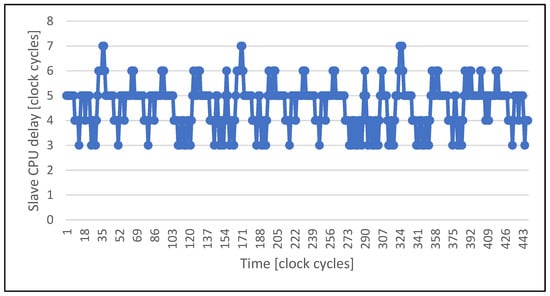
Figure 9.
Trace of the delay between the master and slave cores in VDCLS execution.
4.1. FPGA Results
Table 1 presents the performance comparison between the regular CCRV32ST processor core and the dual-core lockstep implementation using the VDCLS technique. The results were obtained by implementing both processor versions in the Xilinx VCU108 board. As previously noted, the bare fact that stall cycles have to be injected means that the VDCLS performance will be impacted. The extent of this impact depends on the executed software profile, bus utilization, etc. For example, the negative impact on CoreMark execution is much lower than that on Dhrystone. The presented results show that the negative impact is low and depends on the target application.

Table 1.
Performance comparison between regular and VDCLS implementation.
Table 2 presents the FPGA resource utilization comparison between the regular CCRV32ST dual-core processor implementation and the VDCLS one. Every dual-core lockstep implementation requires additional resources, such as error detection logic or switches that reorganize cores and memories on the system busses. In the VDCLS implementation the interrupt and multicore logic is much bigger due to the implementation of VCDLS Controller Module and Interrupt Injection Module. The price of additional 4% system resource utilization is compensated by the flexible split/core processing mode, where lockstep mode ensures fast error detection and makes security attacks more difficult. The processor system components used for comparison are presented in Figure 3. AMBA APB interconnect and peripherals as well as DMA block were excluded from the comparison.
Table 2.
Resources utilization comparison between regular dual core and VDCLS implementation using FPGA VCU108 platform.
4.2. Execution Correlation Results
The execution trace presented in Figure 9 shows that, indeed, the slave core delay does not have to be constant and the VDCLS implementation can execute software correctly. On the other hand, the presented figure shows only a very time-limited trace that is hard to analyze. To overcome this problem, we implemented test logic in the processor core that counts DFFs toggles in the execution stage. We choose the execute stage as the most representative one in the processor pipeline. The execute stage is responsible for the calculation of instruction results, address generation, interrupt and exception evaluation. In the real ASIC design, the toggle count will transform into power consumption trace, the tool that is most commonly used for power analysis attacks []. By having toggle count traces, we could use formula (1) to calculate their correlation with different delays. The first and second formula variables are the toggle count traces of the master and slave cores, respectively. The number of samples represents the simulation time in clock cycles. The function argument d is the offset in clock cycles between the master and slave core traces. We can anticipate that in the classic DCLS approach the execution correlation between the two cores will reach the maximum at the value equal to the number of clock cycles of slave core to master core delay.
where:
- r(d):
- correlation coefficient;
- xi:
- values of first variable;
- yi:
- values of second variable;
- n:
- number of samples;
- d:
- the second variable offset.
The comparison of the execution correlation between master and slave cores in classic DCLS and VDCLS implementation using PC simulation is shown in Figure 10, Figure 11, Figure 12, Figure 13, Figure 14 and Figure 15. For test purposes we choose several algorithms, such as AES (Advanced Encryption Standard), SHA (Secure Hash Algorithm), ECDSA (Elliptic Curve Digital Signature Algorithm) and GF (Galois Field) used in security and cryptographic applications. As predicted, the classic DCLS shows a single strong peak with the maximum value at the delay of two clock cycles. It is caused by the fact that the slave core performs, cycle-by-cycle, exact the same toggles as the master core shifted by two clock cycles. On the other hand, in the VDCLS, even though the slave core executes the same software, the microarchitectural states are changing with more freedom. We can see more or less visible correlation peaks that never reach the maximum value and are located at different delays.
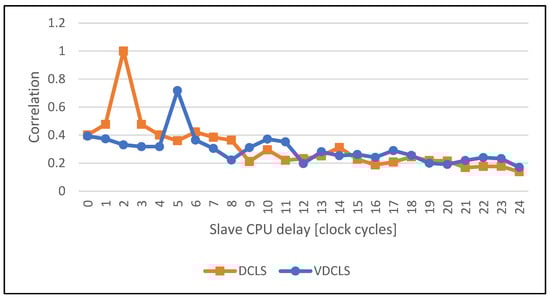
Figure 10.
Comparison of the execution correlation between master and slave CPUs using VDCLS and legacy DCLS technique while executing the SHA algorithm.
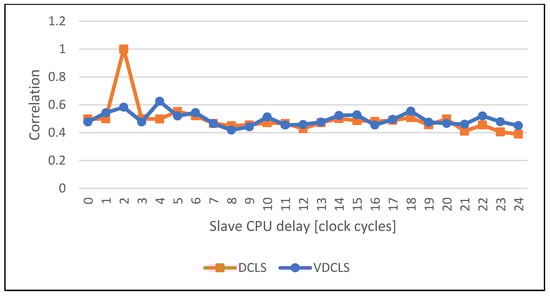
Figure 11.
Comparison of the execution correlation between master and slave CPUs using VDCLS and legacy DCLS technique while executing the HMAC-SHA algorithm.
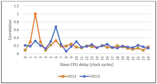
Figure 12.
Comparison of the execution correlation between master and slave CPUs using VDCLS and legacy DCLS technique while executing the CMAC-AES algorithm.
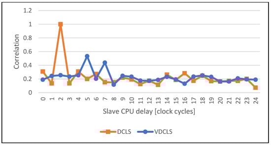
Figure 13.
Comparison of the execution correlation between master and slave CPUs using VDCLS and legacy DCLS technique while executing the EDCSA verification algorithm.
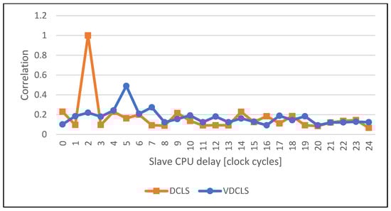
Figure 14.
Comparison of the execution correlation between master and slave CPUs using VDCLS and legacy DCLS technique while executing the EDCSA key compression algorithm.
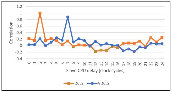
Figure 15.
Comparison of the execution correlation between master and slave CPUs using VDCLS and legacy DCLS technique while executing the Galois field GF (28) functions.
4.3. Dummy Cycles Injection Results
The received results encouraged us to conduct further research on the possibility of flattening the execution correlation between the cores. One of the common techniques for power signature masking is dummy cycle injection []. In the classic DCLS implementation, dummy cycle injection needs to be processed in the same way in both master and slave cores, maintaining the common delay. In the proposed technique, we have a VDCLS Controller Module that already is responsible for stall cycle injection. We improved that module to be able to inject additional dummy cycles using an external LFSR/TRNG generator. The dummy cycle injection is capable of inserting wait states to both master and slave cores independently, and its threshold level is controlled by software.
Figure 16, Figure 17, Figure 18 and Figure 19 show the comparison of execution correlation between master and slave cores with additional dummy cycle injection in the VDCLS implementation. The results were obtained using PC simulation. Dummy cycle injection was enabled using software and set at the approximate level of 6% and 18% of each instruction commit by both cores. We can see a significant decrease in the correlation peak level. In some cases, the peak itself can be also shifted towards different delays.
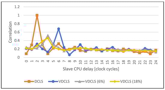
Figure 16.
Comparison of the execution correlation between master and slave CPUs using VDCLS with dummy cycles insertion and legacy DCLS technique while executing the CMAC-AES algorithm.
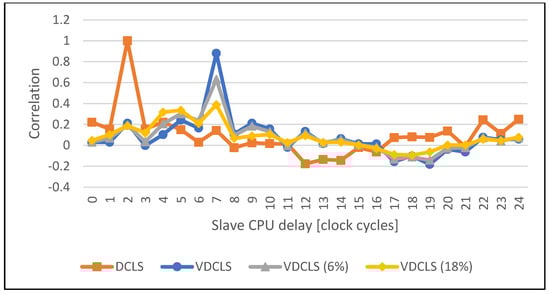
Figure 17.
Comparison of the execution correlation between master and slave CPUs using VDCLS with dummy cycles insertion and legacy DCLS technique while executing the Galois field GF (28) functions.
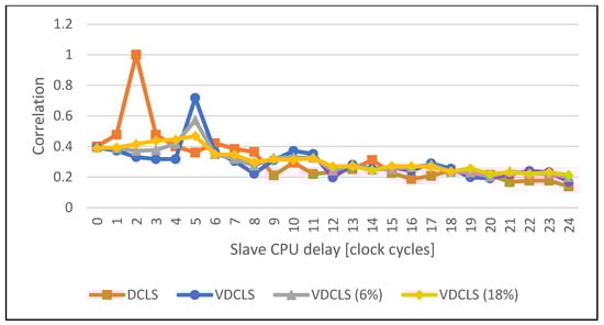
Figure 18.
Comparison of the execution correlation between master and slave CPUs using VDCLS with dummy cycles insertion and legacy DCLS technique while executing the SHA algorithm.
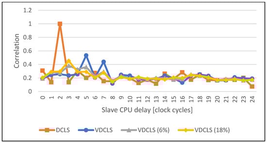
Figure 19.
Comparison of the execution correlation between master and slave CPUs using VDCLS with dummy cycles insertion and legacy DCLS technique while executing the ECDSA verification algorithm.
The low correlation of core execution means that it is hard to distinguish which software instruction is processed at the exact moment by each core. On the other hand, we know that in the longer term, both cores execute exactly the same code and obtain the same results. That means that we will still be able to observe particular power trace patterns introduced by the executed software running on the processor with given microarchitecture. The VDCLS technique was developed for error detection where the introduced variable temporal diversity can enhance the CMF mitigation. However, the use of the proposed method can be extended to security applications, where safety is one of the main requirements. We showed that the VDCLS technique can be easily extended and modified, for example, with random dummy cycle injection. The introduced technique may also be used in conjunction with other power attack countermeasure methods, either software/algorithm based [] or technology based, such as WDDL (Wave Dynamic Differential Logic) or MDPL (Masked Dual-rail with Precharge Logic) [].
5. Failure Analysis
One of the major groups of harmful effects causing malfunction of electronic devices is called Single-Event Effect (SEE) []. While the DCLS technique (and VDCLS as well) introduces redundancy by design, which helps mitigate SEE, the single point and common mode failures require much more attention []. In this section, we briefly describe these failure groups, discuss their mitigation and show simulated results of fault coverage.
5.1. Single Event Effects
By definition, the group of single event effects concerns situations where, at a given time, one functional node (wire, logic gate, memory cell, DFF, etc.) manifests malfunction. The lockstepping technique mitigates such events by design using redundancy. During SEE, only one node in one processor core fails. As a result, the checker module can easily detect mismatches between processor cores and take appropriate actions to prevent further misoperation.
5.2. Common Mode Failures
Common mode failure (CMF) is the result of an event or events located close in time that cause a failure in both redundant blocks []. If both redundant cores experience the same malfunction at the same time, the checker module will not be able to detect such a condition, as the outputs from both cores will match. The most effective way to mitigate CMF is to introduce diversity in both redundant cores. In the classic DCLS and the derivative VDCLS technique, the delay between master and slave cores adds temporal diversity to mitigate CMF. With the delay between the cores, errors are serialized and reach the checker module one after another manifesting themselves as two SEEs that can be easily detected. On the other hand, the CMF can occur naturally, but can also be injected intentionally by the attacker. If the attacker is aware of the underlying hardware and constant delay in DCLS processor, he or she may potentially conduct a set of events located in time in such a way that will cause same malfunction in both delayed cores and prevent the checker module from detecting it. As shown previously in the execution correlation results, with VDCLS, the attacker does not know the current delay between the cores, which makes the fault injection process much more difficult.
5.3. Single Point of Failure
In contrast to CMFs that originate in the protected logic, SPOFs are caused by the logic outside the SoR. One of the most common ways to deal with SPOF is to introduce an additional protection layer consisting of ECC, hardware or software protocol checkers, watchdogs, etc. In contrast to the classic DCLS approach, VDCLS reduces the risk of SPOF by including instruction and data cache controllers to the SoR. More modules inside the SoR leave less unprotected logic that is the source of SPOF.
5.4. Fault Coverage
The aim of the lockstepping technique is to maximize the fault coverage, one of the most important factors that determine reliability. Altogether, 98% mitigation of bit-flips injected into the register file has been reported in [], while the experimental results presented in [] indicate 99.63% error coverage. Moreover, the authors of the system demonstrated in [] claim coverage up to 99.3%. All these results were obtained using a combination of hardware/software approach exploiting checkpointing without full synchronization. On the other hand, [] exploits two processor pipelines executing two virtual cores. The comparison between both pipeline stages occurs every clock cycle resulting in 100% fault coverage. This is the value expected from the classic delayed dual-core lockstep processor, as well as from the presented VDCLS technique.
To evaluate and confirm fault coverage of VDCLS, we adopted the fault injection technique used in []. We prepared a matrix multiplication benchmark that uses random generated 16 × 16 matrices of 32-bit integer elements. During PC simulation, after matrices initialization, an error is injected to a random position of randomly selected register file entry or PC register in the master core. We run the processor design under test (DUT) PC simulation in parallel with golden reference model for covering errors undetected by the Checker Module. We injected 14,068 faults resulting in 7233 (51.41%) errors. Figure 20 shows the percentage of errors caused by the particular registers. Some registers never caused error. This is due to the fact that the compiler does not use all registers, and in some cases, registers are overwritten by the software before a fault activates. Table 3 shows that as expected VDCLS achieves 100% fault coverage.
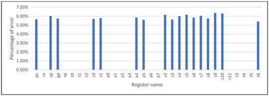
Figure 20.
Percentage of errors caused by register file entries and PC register.
Table 3.
Simulation results of fault injection.
6. Conclusions
In this paper, we showed a novel Variable Delayed Dual-Core Lockstep (VDCLS) technique for error detection. In contrast to the classic DCLS approach, where slave core delay is fixed, we allow the checker core to run freely behind the main core within the constrained boundaries of clock cycles. This increases the temporal diversity needed for CMF mitigation. One of the consequences of the proposed method was to increase the SoR area with the instruction and data cache memories, which reduces SPOF risk. Each core fetches instructions and data to their cache memories using separate requests on the system bus. This additional layer over typical ECC codes significantly hinders side channel manipulation as the attacker would need to intervene in two bus transactions taking place in two hard-to-predict time points. The VDCLS technique was implemented using the CCRV32ST processor core utilizing RISC-V standard “GC” instruction set. The results show a low 4% overhead in system level FPGA resources of VDCLS implementation versus similar dual-core processor. The additional hardware results in a flexible split/lock system where the split mode features high dual-core performance, whereas the lockstep mode ensures fast error detection and makes security attacks more difficult. The performance drawback of the proposed technique comes from the necessity to inject stall cycles to maintain core synchronization. We showed that this negative impact is low and depends on the executing software. In return we are able to flatten the power consumption correlation between the running cores, essential for a wide range of attacks. The design of VDCLS Controller Modules allows random dummy cycles to be injected into each core independently. The presented results show that this step further decreases the correlation peak. The introduced power disruption caused by the variable delay between the processing cores and randomly injected dummy cycles make it more difficult for an attacker to infer about executed code and inject precisely timed faults. Despite the fact that VDCLS is mainly an error detection technique, it can be further enhanced and used jointly with other techniques in order to create safe and secure microprocessor systems.
Author Contributions
Methodology, investigation, validation, visualization, writing—original draft preparation, K.M.; writing—review and editing, funding acquisition, W.A.P. All authors have read and agreed to the published version of the manuscript.
Funding
This research received no external funding.
Data Availability Statement
The data presented in this study are available on request from the corresponding author.
Conflicts of Interest
The authors declare no conflict of interest.
References
- Sierawski, B.D.; Reed, R.A.; Mendenhall, M.; Weller, R.A.; Schrimpf, R.D.; Wen, S.-J.; Wong, R.; Tam, N.; Baumann, R.C. Effects of scaling on muon-induced soft errors. In Proceedings of the 2011 International Reliability Physics Symposium, Monterey, CA, USA, 10–14 April 2011; pp. 3C.3.1–3C.3.6. [Google Scholar]
- ECSS-E-ST-70-11C; Space Engineering—Space Segment Operability. ESA-ESTEC: Noordwijk, The Netherlands, 2008.
- ISO 26262:2018 Road Vehicles—Functional Safety. 2018. Available online: https://www.iso.org/standard/68383.html (accessed on 24 November 2022).
- Oh, N.; Shirvani, P.P.; McCluskey, E.J. Control-flow checking by software signatures. IEEE Trans. Reliab. 2002, 51, 111–122. [Google Scholar] [CrossRef]
- Bashiri, M.; Miremadi, S.G.; Fazeli, M. A Checkpointing Technique for Rollback Error Recovery in Embedded Systems. In Proceedings of the 2006 International Conference on Microelectronics, Dhahran, Saudi Arabia, 16–19 December 2006; pp. 174–177. [Google Scholar]
- Mukherjee, S. Architecture Design for Soft Errors; Morgan Kaufmann Publishers Inc.: San Francisco, CA, USA, 2008. [Google Scholar]
- Iturbe, X.; Venu, B.; Ozer, E.; Das, S. A Triple Core Lock-Step (TCLS) ARM® Cortex®-R5 Processor for Safety-Critical and Ultra-Reliable Applications. In Proceedings of the 2016 46th Annual IEEE/IFIP International Conference on Dependable Systems and Networks Workshop (DSN-W), Toulouse, France, 28 June 2016–01 July 2016; pp. 246–249. [Google Scholar]
- RISC-V International. Available online: https://riscv.org/ (accessed on 20 November 2022).
- Ozer, E.; Venu, B.; Iturbe, X.; Das, S.; Lyberis, S.; Biggs, J.; Harrod, P.; Penton, J. Error Correlation Prediction in Lockstep Processors for Safety-Critical Systems. In Proceedings of the 2018 51st Annual IEEE/ACM International Symposium on Microarchitecture (MICRO), Fukuoka, Japan, 20–24 October 2018; pp. 737–748. [Google Scholar]
- NEC Corporation. Fault Tolerant Server. White Paper, 2017. Available online: https://www.nec.com/en/global/prod/express/collateral/whitepaper/ft_WhitePaper_E.pdf (accessed on 24 November 2022).
- Stratus. FtServer Architecture. Available online: https://www.stratus.com/solutions/platforms/ftserver/ftserver-architecture/ (accessed on 19 November 2022).
- STMicroelectronics. SPC574K72/SPC57EM80 Getting Started. Revision 2. Application Note. 2014. Available online: https://www.st.com/resource/en/application_note/an4389-spc574k72spc57em80-getting-started-stmicroelectronics.pdf (accessed on 23 November 2022).
- NXP Semiconductors. MPC5643L Microcontroller Reference Manual. Rev. 10. 2012. Available online: https://www.nxp.com/files-static/32bit/doc/ref_manual/MPC5643LRM.pdf (accessed on 23 November 2022).
- NXP Semiconductors. e200z4 Power Architecture™ Core Reference Manual. Rev. 0. 2009. Available online: https://www.nxp.com/files-static/32bit/doc/ref_manual/e200z4RM.pdf (accessed on 23 November 2022).
- Texas Instruments. TMS570LC4357 Hercules™ Microcontroller Based on the ARM® Cortex®-R Core. 2017. Available online: https://www.ti.com/lit/ds/spns195c/spns195c.pdf (accessed on 23 November 2022).
- ARM Ltd. Cortex™-R5 Revision: r1p2. Technical Reference Manual. 2011. Available online: https://developer.arm.com/documentation/ddi0460/d/ (accessed on 23 November 2022).
- ARM Ltd. Cortex-M33 Dual Core Lockstep. Version 1.0. Application Note. 2017. Available online: https://developer.arm.com/documentation/ecm0690721/latest (accessed on 23 November 2022).
- Synopsys, Inc. DesignWare ARC Functional Safety Processor IP. Available online: https://www.synopsys.com/designware-ip/processor-solutions/arc-functional-safety-processors.html (accessed on 24 November 2022).
- UltraSoC Technologies Ltd. Cybersecurity and functional safety: The case for embedded analytics. White paper. Available online: https://hc32.hotchips.org/assets/sponsors/UltraSoC/UltraSoC_Safety%20and%20Security%20white%20paper.pdf (accessed on 24 November 2022).
- Sondon, S.; Mandolesi, P.; Masson, F.; Julián, P.; Palumbo, F. A dual core low power microcontroller with openMSP430 architecture for high reliability lockstep applications using a 180 nm high voltage technology node. In Proceedings of the 2013 IEEE 4th Latin American Symposium on Circuits and Systems (LASCAS), Cusco, Peru, 27 February–1 March 2013; pp. 1–4. [Google Scholar]
- Hanafi, A.; Karim, M.; Hammami, A.E. Dual-lockstep microblaze-based embedded system for error detection and recovery with reconfiguration technique. In Proceedings of the 2015 Third World Conference on Complex Systems (WCCS), Marrakech, Morocco, 23–25 November 2015; pp. 1–6. [Google Scholar]
- de Oliveira, Á.B.; Rodrigues, G.S.; Kastensmidt, F.L.; Added, N.; Macchione, E.L.A.; Aguiar, V.A.P.; Medina, N.H.; Silveira, M.A.G. Lockstep Dual-Core ARM A9: Implementation and Resilience Analysis Under Heavy Ion-Induced Soft Errors. IEEE Trans. Nucl. Sci. 2018, 65, 1783–1790. [Google Scholar] [CrossRef]
- Sim, M.T.; Zhuang, Y. A Dual Lockstep Processor System-on-a-Chip for Fast Error Recovery in Safety-Critical Applications. In Proceeding of the 46th Annual Conference of the IEEE Industrial Electronics Society (IECON), Singapore, 18–21 October 2020; pp. 2231–2238. [Google Scholar]
- Doran, H.D.; Lang, T. Dynamic Lockstep Processors for Applications with Functional Safety Relevance. In Proceedings of the 26th IEEE International Conference on Emerging Technologies and Factory Automation (ETFA), Västerås, Sweden, 7–10 September 2021; pp. 1–4. [Google Scholar]
- Kempf, F.; Hartmann, T.; Baehr, S.; Becker, J. An Adaptive Lockstep Architecture for Mixed-Criticality Systems. In Proceedings of the 2021 IEEE Computer Society Annual Symposium on VLSI (ISVLSI), Tampa, FL, USA, 7–9 July 2021; pp. 7–12. [Google Scholar]
- Abate, F.; Sterpone, L.; Lisboa, C.A.; Carro, L.; Violante, M. New Techniques for Improving the Performance of the Lockstep Architecture for SEEs Mitigation in FPGA Embedded Processors. IEEE Trans. Nucl. Sci. 2009, 56, 1992–2000. [Google Scholar] [CrossRef]
- Kasap, S.; Wächter, E.W.; Zhai, X.; Ehsan, S.; McDonald-Maier, K.D. Novel lockstep-based fault mitigation approach for SoCs with roll-back and roll-forward recovery. Microelectron. Reliab. 2021, 124, 114297. [Google Scholar] [CrossRef]
- Rodrigues, C.; Marques, I.; Pinto, S.; Gomes, T.; Tavares, A. Towards a Heterogeneous Fault-Tolerance Architecture based on Arm and RISC-V Processors. In Proceedings of the 45th Annual Conference of the IEEE Industrial Electronics Society (IECON), Lisbon, Portugal, 14–17 October 2019; pp. 3112–3117. [Google Scholar]
- Oleksiak, A.; Cieślak, S.; Marcinek, K.; Pleskacz, W.A. Design and Verification Environment for RISC-V Processor Cores. In Proceedings of the 26th International Conference Mixed Design of Integrated Circuits and Systems (MIXDES), Rzeszow, Poland, 27–29 June 2019; pp. 206–209. [Google Scholar]
- Cieślak, S.; Oleksiak, A.; Marcinek, K.; Pleskacz, W.A. Retargeting the MIPS-II CPU Core to the RISC-V Architecture. In Proceedings of the 26th International Conference Mixed Design of Integrated Circuits and Systems (MIXDES), Rzeszow, Poland, 27–29 June 2019; pp. 261–264. [Google Scholar]
- ChipCraft Sp z o.o. CCRV32ST-C Processor Core Template. Datasheet. 2019. Available online: http://chipcraft-ic.com/download/CCRV32ST-C_template.pdf (accessed on 24 November 2022).
- Randolph, M.; Diehl, W. Power Side-Channel Attack Analysis: A Review of 20 Years of Study for the Layman. Cryptography 2020, 4, 15. [Google Scholar] [CrossRef]
- Clavier, C.; Coron, J.-S.; Dabbous, N. Differential Power Analysis in the Presence of Hardware Countermeasures. In Proceedings of the Second International Workshop, Worcester, MA, USA, 17–18 August 2000; pp. 252–263. [Google Scholar]
- Ostrowski, Ł.; Marcinek, K.; Pleskacz, W.A. Implementation and Comparison of SPA and DPA Countermeasures for Elliptic Curve Point Multiplication. In Proceedings of the 26th International Conference Mixed Design of Integrated Circuits and Systems (MIXDES), Rzeszow, Poland, 27–29 June 2019; pp. 227–230. [Google Scholar]
- Danger, J.-L.; Guilley, S.; Bhasin, S.; Nassar, M. Overview of Dual rail with Precharge logic styles to thwart implementation-level attacks on hardware cryptoprocessors. In Proceedings of the 3rd International Conference on Signals, Circuits and Systems (SCS), Medenine, Tunisia, 6–8 November 2009; pp. 1–8. [Google Scholar]
- Mitra, S.; Saxena, N.R.; McCluskey, E.J. Common-mode failures in redundant VLSI systems: A survey. IEEE Trans. Reliab. 2000, 49, 285–295. [Google Scholar] [CrossRef]
- Peña-Fernández, M.; Serrano-Cases, A.; Lindoso, A.; García-Valderas, M.; Entrena, L.; Martínez-Álvarez, A.; Cuenca-Asensi, S. Dual-Core Lockstep enhanced with redundant multithread support and control-flow error detection. Microelectron. Reliab. 2019, 100–101, 113447. [Google Scholar] [CrossRef]
- Aviles, P.M.; Lindoso, A.; Belloch, J.A.; Garcia-Valderas, M.; Morilla, Y.; Entrena, L. Radiation Testing of a Multiprocessor Macrosynchronized Lockstep Architecture With FreeRTOS. IEEE Trans. Nucl. Sci. 2022, 69, 462–469. [Google Scholar] [CrossRef]
Disclaimer/Publisher’s Note: The statements, opinions and data contained in all publications are solely those of the individual author(s) and contributor(s) and not of MDPI and/or the editor(s). MDPI and/or the editor(s) disclaim responsibility for any injury to people or property resulting from any ideas, methods, instructions or products referred to in the content. |
© 2023 by the authors. Licensee MDPI, Basel, Switzerland. This article is an open access article distributed under the terms and conditions of the Creative Commons Attribution (CC BY) license (https://creativecommons.org/licenses/by/4.0/).