Article

Recovery Effect of Hot-Carrier Stress on γ-ray-Irradiated 0.13 μm Partially Depleted SOI n-MOSFETs

1
School of Computer Science and Engineering, Southwest Minzu University, Chengdu 610041, China
2
China Academy of Launch Vehicle Technology, Beijing 100076, China
*
Authors to whom correspondence should be addressed.
Electronics 2023, 12(20), 4233; https://doi.org/10.3390/electronics12204233
Submission received: 6 September 2023 / Revised: 28 September 2023 / Accepted: 28 September 2023 / Published: 13 October 2023
(This article belongs to the Special Issue Radiation Effects of Advanced Electronic Devices and Circuits)

Abstract

:
Many silicon-on-insulator (SOI) metal–oxide–semiconductor field-effect transistors (MOSFETs) are used in deep space detection systems because they have higher radiation resistance than bulk silicon devices. However, SOI devices have to face the double challenge of radiation and conventional reliability problems, such as hot carrier stress, at the same time. Thus, we wondered whether there is any interaction between reliability degradation and irradiation damage. In this paper, the effect of hot-carrier injection (HCI) on γ-ray-irradiated partially depleted (PD) SOI n-MOSFETs with a T-shaped gate structure is investigated. A strange phenomenon that accelerated the annealing effect on irradiation devices caused by HCI in 5 s was observed. That is, HCI has fast recovery ability on the irradiated narrow-channel n-MOSFETs. We explain the physical mechanism of this recovery effect qualitatively. Moreover, we designed a comparable experiment to evaluate the effect on the wide-channel devices. These results show that the narrow-channel devices are more sensitive to irradiation and HCI effects than wide-channel devices.

1. Introduction

The development of space electronics technology has traditionally been significantly influenced by the commercial semiconductor industry. The development of metal–oxide–semiconductor (MOS) technology and, in particular, complementary metal–oxide–semiconductor (CMOS) technology, as a dominant commercial technology, have been used to extend the lifespan of devices used in deep space systems [1,2,3,4,5]. Recently, SOI technology has seen widespread applications in the aerospace sector due to its exceptional resistance against transient ionizing radiation, such as single-event effects [6]. However, there is a potential problem associated with the relatively thick buried oxide (BOX), which is sensitive to the total ionizing dose (TID) effect [7,8,9]. Radiation-induced trapped charges build up in the gate oxide, which causes a shift in the threshold voltage (that is, a change in the voltage that must be applied to turn the device on). In other words, the threshold of the back gate would change with the irradiation dose. Although in practical circuits, the back gate is typically grounded, these devices conduct as the threshold of the back gate drifts below zero, leading to a large channel leakage current [10,11,12]. If this shift is large enough, the device cannot be turned off, even with zero voltage applied, and the device is suspected to have failed by entering depletion mode.
Furthermore, devices operating in this environment face not only the challenge of the irradiation environment but also issues with conventional reliability, such as hot carrier stress when they are deployed in deep space missions. In many cases, the HCI effect is regarded as one of the most important factors that limit the lifespan of very large-scale integration (VLSI) circuits and maximal devices. Hot carriers may yield interface traps at Si/SiO2 interface, be trapped in the oxide, or generate new oxide traps, resulting in effects such as threshold voltage (VT) drift, transconductance (Gm) degradation, and an increase in channel leakage current [13]. Both radiation and HCI effects can degrade the device’s performance over time and, ultimately, invalidate the device or circuit [14,15]. Devices exposed to deep space environments face the dual challenges of TID irradiation and HCI effects at the same time, both of which degrade the devices’ performance by introducing trapped charges into the oxide layer or the oxide/bulk interface. Thus, we wondered whether there is any interaction between reliability degradation and irradiation damage, and whether the lifespan of devices with 0.13 μm PD SOI technology could be further decreased by this interaction. In fact, there are researchers who have explored potential synergistic effects or correlations between hot-carrier effects and TID irradiation in PD SOI MOSFETs [16,17,18,19,20]. Silvestri et al. [21,22] investigated how X-ray exposure impacts the long-term reliability of 130 nm n-MOSFETs as a function of device geometry and irradiation bias conditions. The experimental results presented the opposite effect to the degradation during subsequent hot-carrier injection. Increasing the bias during irradiation slightly reduces the impact on subsequent electrical stress in core MOSFETs. Qi-wen Zheng et al. [23] carried out total-dose irradiation on the hot-carrier reliability of 65 nm n-MOSFETs. The experimental results showed that hot-carrier degradation on irradiated narrow-channel n-MOSFETs are greater than on those without irradiation. Jing-hao Zhao et al. [24] measured the enhancement effect on the degradation of gate voltage, Gm, and IDsat during hot carrier stress in both T-gate and H-gate SOI p-MOSFETS irradiated by γ-rays. It was found that TID-induced interface states strengthen the process of hot electron injection into the gate oxide, while the radiation-induced weakening of the Si/SiO2 interface aggravates the generation rate of the interface defects. Previous studies have shown that HCI degradation is particularly important in n-MOSFETs, because there are higher electric fields and impact ionization near the drain region as compared to p-MOSFETs [25,26,27].
However, due to the existence of the BOX layer, the mechanism of irradiation and HCI effects on SOI devices is more complex than on bulk silicon devices. We thought that there may be an interaction between reliability degradation and irradiation damage. So, we carried out HCI tests on γ-ray-irradiated PD SOI n-MOSFETs to verify this idea. During the experiments, a strange phenomenon was observed. The experimental results show that TID leads to a high off-state leakage (Ioff) current and the obvious negative drift of the threshold voltage. Focusing on the irradiation devices, the parameters—especially the Ioff—cannot return to their initial values after 190 h of annealing at room temperature (RT). But the results of the HCI experiments show that the Ioff almost returned to its initial value during the HCI experiment within 5 s. The physical mechanism of this phenomenon is the core content of this paper.
The structure of this paper is organized as follows: Section 1 reviews the background of research on MOSFETs with bulk and SOI processes when they are subjected to radiation and hot carrier stress. Section 2 introduces the device and presents the experimental details. Section 3 discusses the experimental results and analyzes their physical mechanisms. Here, we explain the mechanism of this recovery effect qualitatively. Furthermore, we provide some methods to reduce the value shift of the device characteristics when the devices are used in harsh environments. Finally, Section 4 concludes the whole study.

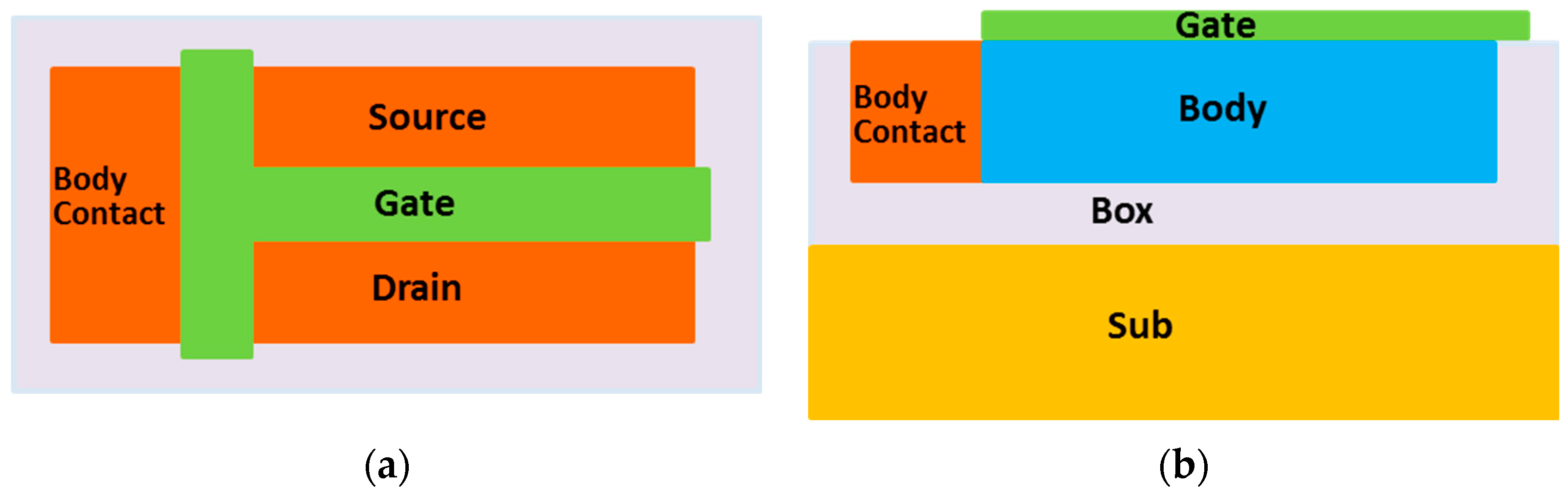
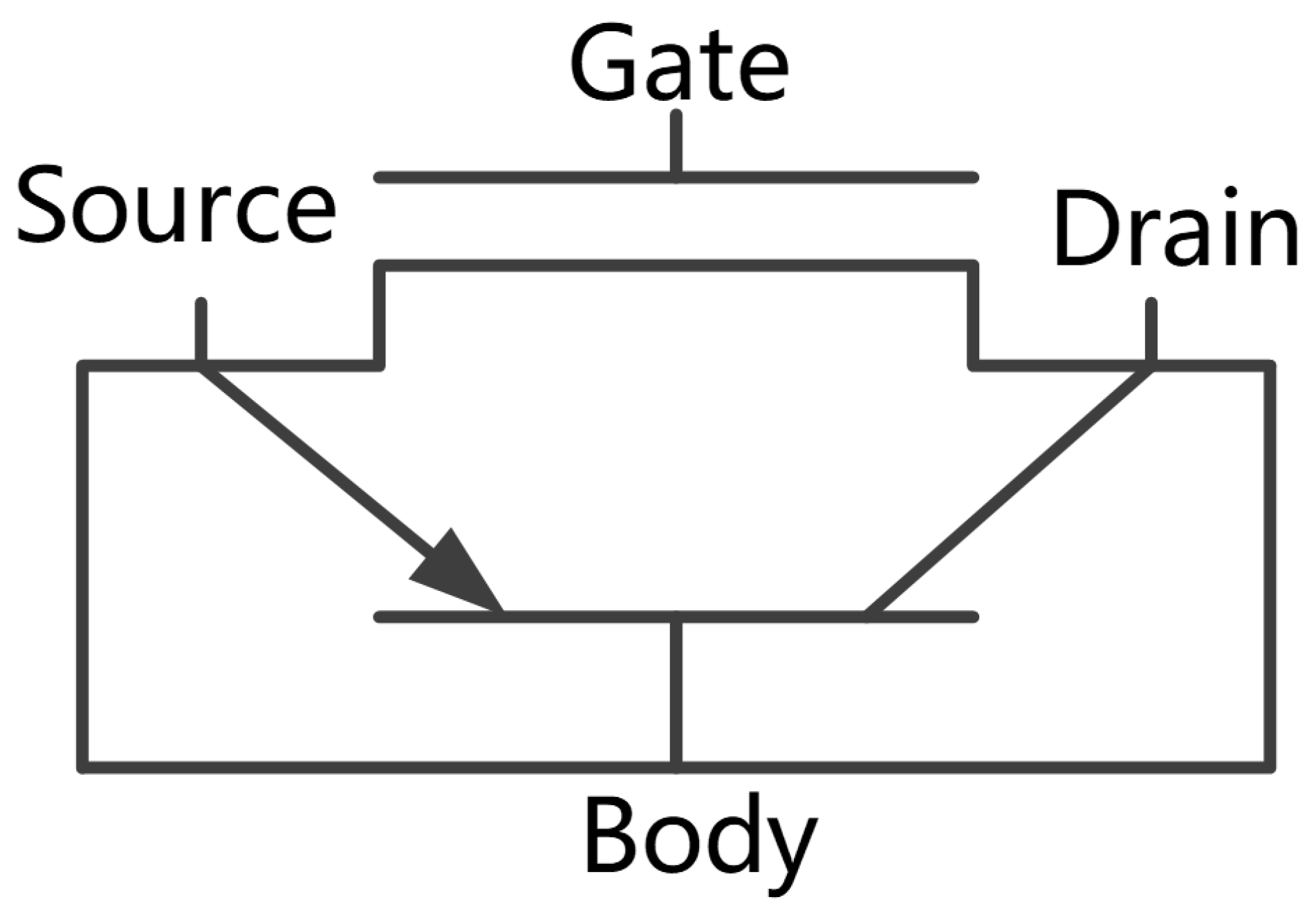
2. Device and Experimental Details

The I/O n-MOSFETs used in this paper were fabricated using 130 nm PD SOI technology [28] in the Center of Materials Science and Optoelectronics Engineering, University of Chinese Academy of Sciences (in Shanghai, China). Processing was performed on a 200 mm diameter UNIBOND® wafer from SOITEC (in Bernin, France) with a 100 nm top Si film and a 145 nm BOX. The body contacts of all transistors were introduced by a T-shaped gate layout, as shown in Figure 1. The gate oxide thickness is 1.8 nm. In this study, two kinds of n-MOSFETs with different channel widths were used in our experiments. The structure parameter of the narrow channel devices was W/L = 0.15 μm/0.35 μm, and the other structure parameter of the wide channel devices was W/L = 10 μm/0.35 μm. Their working voltage was VDS = VGS = 3.3 V, and their doping concentration in the body was about ~1017 cm−3. All the devices were 24-pin DIP-packaged. Three devices were used in our experiments at the same time.
The γ-ray radiation experiments were carried out at the Xinjiang Technical Institute of Physics and Chemistry, Chinese Academy of Sciences, using 60Co-γ as the radiation source. Before the radiation experiments, we tested the initial parameters of these n-MOSFETS. During the γ-ray radiation process, all devices worked on a bias voltage with VGS = 3.3 V. Other pins were grounded at the same time. The samples were irradiated to 2000 Gy (Si) with a dose rate of 0.5 Gy (Si)/s. After irradiation, the devices were annealed for 190 h at room temperature (25 °C), and they kept the same working conditions as the irradiation process. Then, the devices were sent to hot carrier stress experiments. All the electrical tests were performed using a Keithley 4200 B semiconductor test system at room temperature.
According to Joint Electron Device Engineering Council JESD28-A titled “A Procedure for Measuring N-Channel MOSFET Hot Carrier-Induced Degradation under DC Stress”, the bias gate voltage was selected as corresponding to the voltage of the peak substrate current during hot carrier stress experiments. Here, the gate voltage was set to 3.3 V. Additionally, the drain voltage was set to 4.45 V (135% operating voltage) to generate the maximum number of carriers due to impact ionization. Other pins were grounded. Two points including 5 s and 5000 s during hot carrier stress were selected to interrupt electrical stress for the main parameter test.

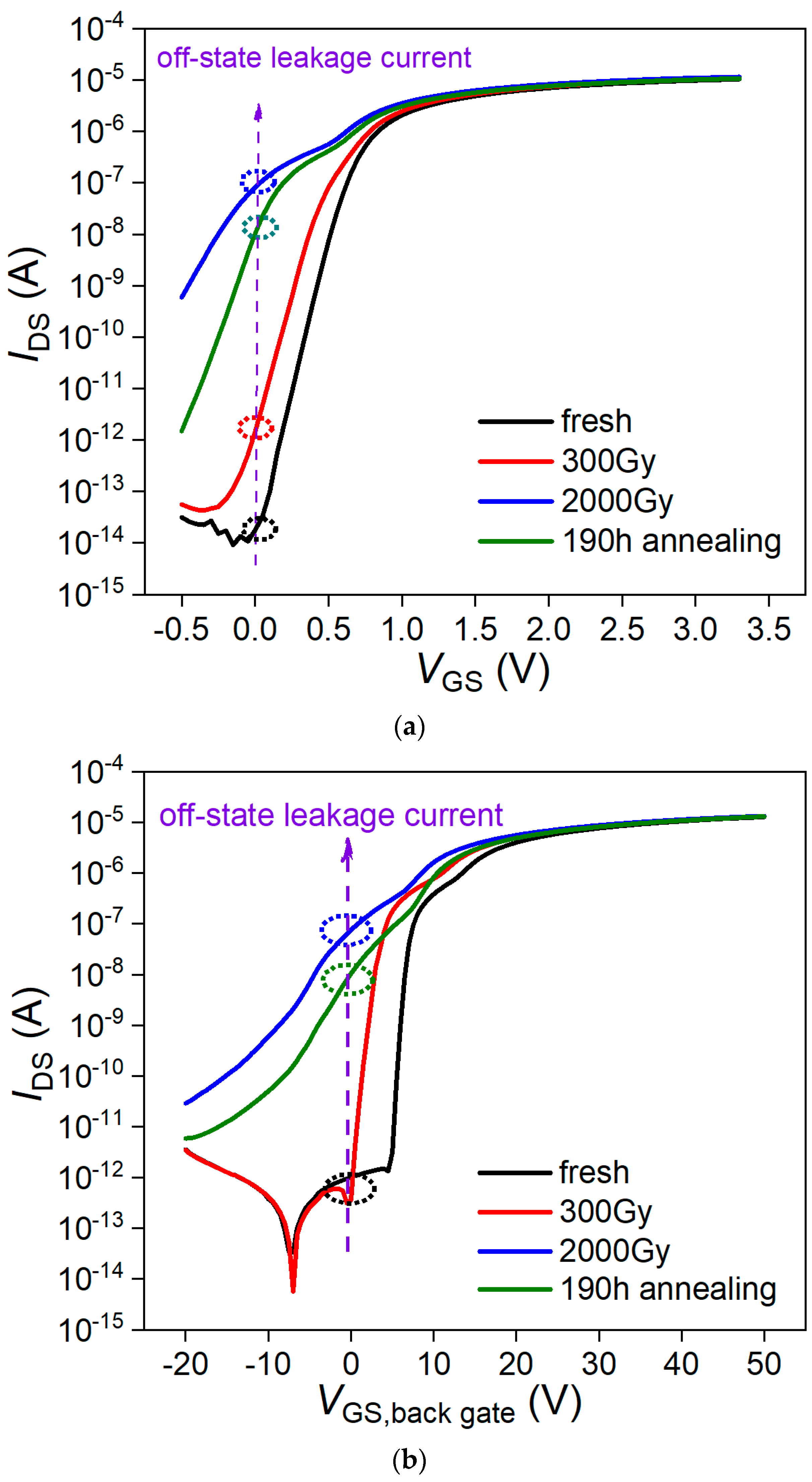
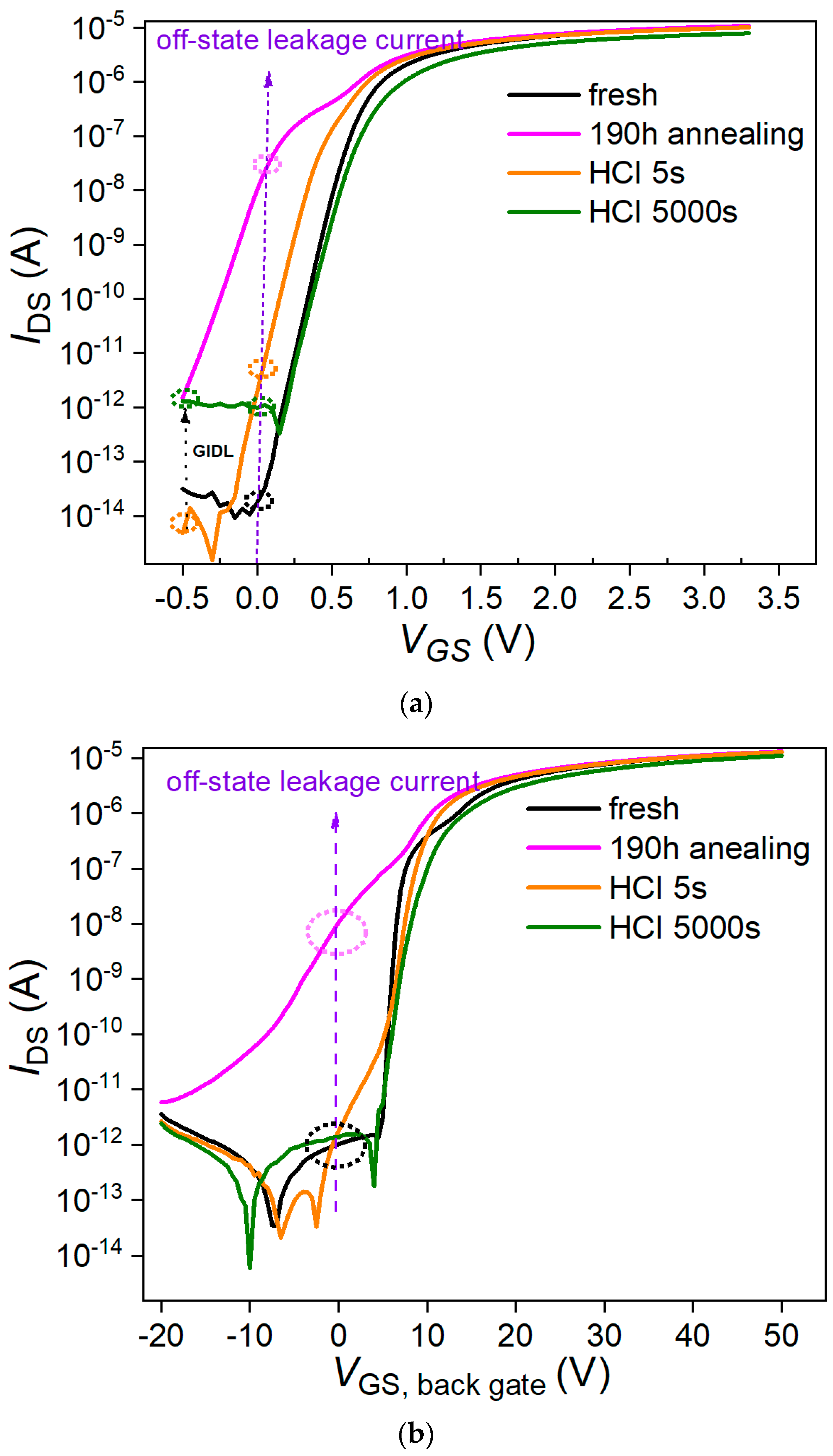
3. Results and Discussion

The front gate and back gate linear area transfer characteristics of narrow channel devices (W/L = 0.15 μm/0.35 μm) before and after irradiation and 190 h RT annealing are shown in Figure 2a,b. We were able to determine that the magnitude of off-state leakage current Ioff for irradiated devices is about 5~6 orders larger than that of the non-irradiated ones.
Based on the results shown in Figure 2, it is believed that the radiation-induced oxide trap charge in the shallow trench isolation (STI) caused the Ioff. As reported in Refs. [1,7], parts of the charges in the inversion top Si film are no longer controlled by the main transistor gate, resulting in a negative threshold shift in the main transistor, which can increase the channel current significantly.
Figure 3 shows the electrical equivalent structure activated by irradiation for the PD SOI MOSFET. The primary parasitic element that contributes to the primary MOS transistor is the parasitic bipolar transistor. The floating body node serves as the base of this parasitic bipolar transistor and can be activated by irradiation that forward biases the body–source diode. To prevent its activation, the body region can be connected to the source potential or be grounded. By doing so, the charge generated by radiation in the body is discharged through the “body tie”. As a result, the body potential is no longer in a floating state [29,30].
A previous work [29] demonstrated that nearly all of the radiation-generated holes that manage to avoid immediate recombination become ensnared within the bulk of the oxide, specifically at deep trap sites near their source. Once trapped, a portion of these holes gradually reverts to a neutral state through the thermal emission of electrons from the oxide valence band at room temperature. Besides hole entrapment, electrons are also captured throughout the entirety of the buried oxide. Most of these trapped electrons are thermally released within one second following a radiation pulse. Subsequent to electron release, the resulting charge is predominantly characterized by a high concentration of positively trapped holes, resulting in significant negative shifts in the threshold voltage of the back gate transistors.
In order to evaluate the impact of the annealing effect, a 190 h RT annealing process is applied to irradiated devices under the same bias voltage as irradiation. As shown in Figure 2, the value of Ioff decreases by about one order after a process of 190 h RT annealing. However, the gap is still considerable compared with the initial value. Here, the thermal emission mechanism of annealing at RT is explained as follows [7].
Φ m ( t ) = k T q · ln [ A T 2 t ]
where Φm(t) presents the energy boundaries of thermal emission, K is the Boltzmann constant, T is the absolute temperature, q is the elementary charge, t is the time factor, and A presents the constant of the capture cross-section. Since our experiments were performed at room temperature, most thermal emission electrons have energies lower than those required to escape deep energy traps. Consequently, these deep energy traps continue to capture holes, leading to the observed outcome illustrated in Figure 2. In other words, the crucial parameters for irradiated n-MOSFETs cannot be restored to their initial values through annealing at room temperature.
When these devices are utilized in the harsh conditions of deep space, they are simultaneously exposed to both radiation and hot carrier stress. It is crucial to investigate the synergistic effects arising from the combination of radiation and the HCI effect. To explore this proposal, we carried out a series of HCI tests on SOI n-MOSFETs post-irradiation. Based on the experimental results, we also identified the phenomenon of gate-induced drain leakage (GIDL), as shown in Figure 4a. It can be seen that GIDL current experiences significant increases after the 5000 s HCI test. The observed increase in post-stress GIDL current is distinctly different from that induced by oxide traps because oxide traps only induce GIDL current transients over a time scale of seconds. So, this should be dependent on the amount of interface traps created during stress [25,31]. In other words, an additional conduction mechanism involving interface traps should be possible after the hot electron stress. Surprisingly, an interesting phenomenon emerged after a 5 s HCI experiment. In the back gate transistor, the curve of Ioff nearly returns to its initial value, as shown in Figure 4b.
Focusing on the experiment phenomena, we believe they are a result of the synergistic effect of radiation and the HCI effect. This enhanced synergistic effect has been proved by Hang. Zhou et al. [27] carried out a compared example using irradiated and unirradiated 0.13 μm PD SOI n-MOSFETs and tested front gate Ids–Vgs curves before and after 3000 s of hot carrier stress. According to the experimental results, it is obvious that irradiated samples display a larger threshold voltage shift during stress time than un-irradiated samples. The threshold shift of an irradiated device is 108 mV after 3000 s stress, while the threshold shift of an unirradiated device is 46 mV.
In this paper, these two effects cause these processes’ complexity. The Ioff caused by radiation induces an oxide trap charge, and the subsequent effects of annealing as a result of the channel-hot electronics leap over the barrier of the Si/SiO2 interface. If electrons collide during travel, they may be incident in the BOX or gate oxide layer. The diagram sketch can be seen in Figure 5a,b.
Moreover, it is important to note that the channel electrons acquire a higher average energy during HCI stress. This increased energy facilitates the annealing of deep-level oxide trap charges, which is shown in Figure 6. The oxide trap charges within the STI region undergo rapid annealing as electrons are injected into them. This electron injection occurs when a high voltage is applied during the HCI test, generating enough hot carriers within the channel. These hot carriers will cross the Si/SiO2 barrier and inject the silicon oxide layer, resulting in the annealing of deep-level oxide trap charges. The corresponding band diagram is depicted in Figure 6, where Xm represents the tunneling front, t presents the time factor, α relates to the attempt frequency for escaping traps, and β is associated with the tunneling barrier [7].
Furthermore, it is essential to note that utilizing a simple tunneling front model for cases involving traps distributed in energy due to HCI may not be entirely accurate, as the tunneling barrier β varies with trap depth. However, for the sake of practicality and the development of a simplified predictive methodology, this effect is considered negligible.
Here, we demonstrate that electrons obtain energy W if electron scattering does not occur during the drift from the source to the drain. Additionally, W can be calculated as follows:
W = qU
When the VDS is set to 4.45 V, the W is equal to 4.45 eV. Because the Si/SiO2 interfacial potential barrier for electrons is 3.15 eV [32,33], high energy-electrons can pass through Si/SiO2 easily. However, it is possible that when the devices work under the normal voltage (3.3 V), the electrons in the channel can still obtain enough energy (3.3 eV) to cross the Si/SiO2 interfacial potential barrier. In this case, we have to calculate the probability of electrons that could pass through Si/SiO2 quantitatively. Here, the probability of electrons in the channel drift distance d without scattering is e d / λ , where λ presents the mean free path of electrons. In silicon, λ = 10.5 nm. The channel length of n-MOSFETs in the test is 0.35 μm. We define P1 as the probability of electrons in the channel drift distance d1, which obtained 3.15 eV energy, and we define P2 as the probability of electrons in the channel drift distance d2 without scattering.
Assuming the electric field in the channel is uniformly distributed, the normal working voltage of the device is set to 3.3 V, and the applied voltage for hot carrier stress experiments is 4.45 V. When the device operates at 4.45 V, the shortest path that electrons need to pass through to obtain energy of 3.15 eV is d1 = (3.15/4.45) × 0.35 μm = 0.24 μm. When the device operates at working voltage, the shortest path that electrons need to pass through to obtain energy of 3.15 eV is d2 = (3.15/3.3) × 0.35 μm = 0.334 μm. It is worth noting that in the context mentioned above, the “shortest path” implies that electrons undergo no scattering or collisions along their trajectory.
Based on these calculations, the ratio of P1/P2 can be obtained as follows:
P 1 / P 2 = e ( d 1 / λ + d 2 / λ ) 8100
Based on this result, the number of hot carrier injections into the STI of devices under HCI stress is 8100 times higher than it is under normal stress. In this case, HCI has a faster recovery capability.
The HCI effect on n-MOSFETs parameters’ degradation is a long-term process for the device’s reliability. Typically, it causes decreased circuit speed rather than catastrophic failure. In this paper, sensitive parameters such as VT, Gm, and IDsat are commonly monitored to identify performance changes. The devices we used in these experiments are ultra-thin gates, so the influence of the oxide trap charge is very small. As shown in Figure 7 and Figure 8, the curve of Gm–VGS and Gm (Max) in different states can be observed.
In order to extract VT, the Gm extrapolation method in the linear region was used in this study [34,35]. This method suggests that the threshold voltage corresponds to the gate voltage axis intercept of the linear extrapolation of the Gm–VGS characteristics at its maximum first derivative (slope) point. As shown in Figure 9, the extract threshold voltage shift of PD SOI n-MOSFET is −100 mV after 2000 Gy irradiation and is restored to −70 mV after 190 h of annealing. When the devices were tested in the HCI test, the threshold voltage shift was −50 mV after 5 s HCI and 50 mV after 5000 s HCI. The change trend of ∆VT can be observed in the inline image of Figure 9.
The expression of the threshold voltage shift is shown as follows [7]:
Δ V T = Δ V T o t + Δ V T i t
where ΔVTot is caused by oxide traps and ΔVTit is caused by the interface state. For n-MOSFETs, ΔVTit is negative when the interface state level is below the Fermi level under a positive gate voltage. Based on the above formulation, we believe that the degradation of VT is a result of the oxide trap charge and interface states. Under HCI stress, channel electrons are accelerated to very high energy and lead to an injection into the oxide gate. Some chemical bonds at the Si/SiO2 interface are broken for the hot carrier transfer energy to the lattice through phonon emission. Some carriers are trapped in the SiO2 layer. The trapping or bond breaking creates oxide charge and interface traps that affect the channel carrier mobility and reliability of the gate oxide. The impact on IDsat is shown in Figure 10.
The theme of this paper revolves around the examination of the synergistic effects of narrow-channel transistors. As depicted in Figure 9, the irradiation has a pronounced impact on the threshold voltage of these narrow-channel devices, causing a substantial negative shift. This shift is particularly notable due to the thinness of the top silicon film, which is less than twice the width of the maximum depleted region. This thin film is a consequence of the low doping concentrations in the substrate region.
Consequently, depletion regions emerge independently at both the front and back interfaces. These regions have the potential to interconnect when a sufficient amount of charge becomes trapped in the BOX layer. Similar to fully depleted SOI devices, the radiation-induced charges trapped in the BOX layer alter the electric potential within the substrate region of PD SOI devices. This alteration results in a negative threshold shift at the front gate. Additionally, it is important to note that narrow devices exhibit heightened sensitivity to the charge trapped within the silicon dioxide layer in the shallow trench isolation (STI) along the channel.
To prove this proposal, wide-channel 0.13 μm PD SOI n-MOSFETs (W/L = 10 μm/0.35 μm) with the same process are used for γ-ray radiation and HCI experiments. The front gate and back gate IDS–VGS curves of wide channel devices under 2000 Gy irradiation and 3000 s of HCI stress are shown in Figure 11. We found that the Ioff of the front gate and back gate transistors changed by about three orders after 2000 Gy irradiation, and it almost recovered to its initial value after HCI experiments.
According to the results shown in Figure 12, the threshold voltage VT is negatively shifted by radiation-induced positive charges trapped in BOX, while the gate threshold is positively shifted by channel hot carrier stress. The change trend of ∆VT can be shown in the internal image of Figure 12. Compared to the narrow-channel devices, the VT of wide-channel devices is insensitive to irradiation and HCI effects.
To minimize the shift in device characteristics, we think the following methods could be used for combined conditions of radiation and HCI. Faced with the issue of radiation hardness, an H-gate structure design is an effective technology to replace the T-gate design. In the H-gate device, its side wall oxide is completely eliminated, and the radiation resistance performance of the device is greatly improved. However, this design method requires more layout area. For the unique BOX layer of SOI devices, radiation hardness methods such as the Si injection process can be used to suppress or compensate for the effects of radiation-induced positive charges.
For 0.13 μm process technology, a lightly doped drain (LDD) structure design can be used to suppress the HCI effect. That could avoid the design concept of extremely short-channel devices. In addition, some special factories will perform special passivation processes on the Si/SiO2 interface, such as replacing H+ with F+, because the Si–F bond has much stronger bond energy than Si–H. In this case, under the same thermal electron collision, F+-passivated devices will generate fewer dangling bonds, effectively controlling the generation of Nit.

4. Conclusions

This paper discusses radiation reliability screens for 0.13 μm PD SOI n-MOSFETs used in applications with HCI environments. The results show that the HCI effect has a recovery effect on the long-term reliability of the n-MOSFETs when applied to a space environment. In our opinion, the physical mechanism of this effect is that the high-energy electrons produced by HCI lead to deep-level oxide trap charge annealing, which leads to the almost complete elimination of Ioff within a few seconds. At the same time, the high-energy electrons injected into the SiO2 layer led to many interface states being produced, which leads to the degradation of the Gm, VT, and IDsat. There is a combined effect between HCI and TID. Further, we designed a comparable experiment to evaluate the effect on wide-channel devices. These results show that narrow-channel devices are more sensitive to irradiation and HCI. Based on the results presented in this work, it is useful to place SOI MOSFETs in a biased working state when they are used in space electronic systems, as this will extend their lifespan.

Author Contributions

Conceptualization and writing—original draft preparation, L.L.; methodology, Z.C., formal analysis, C.J. All authors have read and agreed to the published version of the manuscript.

Funding

This research was funded by the Southwest Minzu University Research Startup Fund, grant number RQD2021088, and the Fundamental Research Fund for the Central Universities—Southwest Minzu University, grant number 2021NQNCZ10.

Data Availability Statement

Not applicable.

Acknowledgments

The authors thank Hang Zhou of the Microsystem and Terahertz Research Center, CAEP, for his kind help in data analysis and discussion.

Conflicts of Interest

The authors declare no conflict of interest.

Nomenclature

PD SOIPartially Depleted Silicon-On-Insulator
MOSFETMetal–Oxide–Semiconductor Field Effect Transistor
HCIHot Carrier Injection
MOSMetal Oxide Semiconductor
CMOSComplementary Metal–Oxide–Semiconductor
TIDTotal Ionizing Dose
BOXBuried Oxide
VLSIVery Large-Scale Integration
RTRoom Temperature
GIDLGate-Induced Drain Leakage
STIShallow Trench Isolation

References

  1. Oldham, T.R.; McLean, F.B. Total ionizing dose effects in MOS oxides and devices. IEEE Trans. Nucl. Sci. 2003, 50, 483–499. [Google Scholar] [CrossRef]
  2. Brewer, R.M.; Zhang, E.X.; Gorchichko, M.; Wang, P.F.; Cox, J.; Moran, S.L.; Ball, D.R.; Sierawski, B.D.; Fleetwood, D.M.; Schrimpf, R.D.; et al. Total ionizing dose responses of 22-nm FDSOI and 14-nm bulk FinFET charge-trap transistors. IEEE Trans. Nucl. Sci. 2021, 68, 677–686. [Google Scholar] [CrossRef]
  3. Jiang, R.; Zhang, E.X.; McCurdy, M.W.; Wang, P.; Gong, H.; Yan, D.; Schrimpf, R.D.; Fleetwood, D.M. Dose-rate dependence of the total-ionizing-dose response of GaN-based HEMTs. IEEE Trans. Nucl. Sci. 2018, 66, 170–176. [Google Scholar] [CrossRef]
  4. Wang, P.F.; Zhang, E.X.; Chuang, K.H.; Liao, W.; Gong, H.; Arutt, C.N.; Ni, K.; Mccurdy, M.W.; Verbauwhede, I.; Bury, E.; et al. X-ray and proton radiation effects on 40 nm CMOS physically unclonable function devices. IEEE Trans. Nucl. Sci. 2018, 65, 1519–1524. [Google Scholar] [CrossRef]
  5. Wang, P.F.; Zhang, E.X.; Fleetwood, D.M.; McCurdy, M.W.; Lin, J.-T.; Alles, M.L.; Davidson, J.L.; Alphenaar, B.W.; Schrimpf, R.D. Effects of Charge Generation and Trapping on the X-ray Response of Strained AlGaN/GaN HEMTs. In Proceedings of the 2021 IEEE 14th International Conference on ASIC (ASICON), Kunming, China, 26–29 October 2021; IEEE: Piscataway, NJ, USA, 2021; pp. 1–4. [Google Scholar] [CrossRef]
  6. Musseau, O. Single-event effects in SOI technologies and devices. IEEE Trans. Nucl. Sci. 1996, 43, 603–613. [Google Scholar] [CrossRef]
  7. McWhorter, P.; Miller, S.; Miller, W. Modeling the anneal of radiation-induced trapped holes in a varying thermal environment. IEEE Trans. Nucl. Sci. 1990, 37, 1682–1689. [Google Scholar] [CrossRef]
  8. Liu, B.; Li, Y.; Wen, L.; Zhang, X.; Guo, Q. Effects of Hot Pixels on Pixel Performance on Backside Illuminated Complementary Metal Oxide Semiconductor (CMOS) Image Sensors. Sensors 2023, 23, 6159. [Google Scholar] [CrossRef]
  9. Li, X.; Cui, J.; Zheng, Q.; Li, P.; Cui, X.; Li, Y.; Guo, Q. Study of the Within-Batch TID Response Variability on Silicon-Based VDMOS Devices. Electronics 2023, 12, 1403. [Google Scholar] [CrossRef]
  10. Zhang, Y.W.; Huang, H.X.; Bi, D.W.; Tang, M.; Zhang, Z. Investigation of unique total ionizing dose effects in 0.2 µm partially-depleted silicon-on-insulator technology. Nucl. Instrum. Methods Phys. Res. Sect. A Accel. Spectrometers Detect. Assoc. Equip. 2014, 745, 128–132. [Google Scholar] [CrossRef]
  11. Fan, S.; Hu, Z.-Y.; Zhang, Z.-X.; Ning, B.-X.; Bi, D.-W.; Dai, L.-H.; Zhang, M.-Y.; Zhang, L.-Q. Total ionizing dose induced single transistor latchup in 130-nm PDSOI input/output NMOSFETs. Chin. Phys. B 2017, 26, 036103. [Google Scholar] [CrossRef]
  12. Huang, H.-X.; Bi, D.-W.; Peng, C.; Zhang, Y.-W.; Zhang, Z.-X. The Enhanced Role of Shallow-Trench Isolation in Ionizing Radiation Damage of Narrow Width Devices in 0.2 μm Partially-Depleted Silicon-on-Insulator Technology. Chin. Phys. Lett. 2013, 30, 080701. [Google Scholar] [CrossRef]
  13. Zheng, Q.-W.; Cui, J.-W.; Zhou, H.; Yu, D.-Z.; Yu, X.-F.; Lu, W.; Guo, Q.; Ren, D.-Y. Analysis of functional failure mode of commercial deep sub-micron SRAM induced by total dose irradiation. Chin. Phys. B 2015, 24, 106106. [Google Scholar] [CrossRef]
  14. Yeh, W.-K.; Wang, W.-H.; Fang, Y.-K.; Chen, M.-C.; Yang, F.-L. Hot-carrier-induced degradation for partially depleted SOI 0.25–0.1/spl mu/m CMOSFET with 2-nm thin gate oxide. IEEE Trans. Electron. Devices 2002, 49, 2157–2162. [Google Scholar] [CrossRef]
  15. Cui, J.; Xue, Y.; Yu, X.; Ren, D.; Lu, J.; Zhang, X. Total dose irradiation and hot-carrier effects of sub-micro NMOSFETs. J. Semicond. 2012, 33, 014006. [Google Scholar] [CrossRef]
  16. Rafí, J.M.; Simoen, E.; Mercha, A.; Hayama, K.; Campabadal, F.; Ohyama, H.; Claeys, C. Electrical stress on irradiated thin gate oxide partially depleted SOI nMOSFETs. Microelectron. Eng. 2007, 84, 2081–2084. [Google Scholar] [CrossRef]
  17. Huang, D.H.; King, E.E.; Wang, J.J.; Ormond, R.; Palkuti, L. Correlation between channel hot-electron degradation and radiation-induced interface trapping in N-channel LDD devices. IEEE Trans. Nucl. Sci. 1991, 38, 1336–1341. [Google Scholar] [CrossRef]
  18. Dai, L.; Liu, X.; Zhang, M.; Zhang, L.; Hu, Z.; Bi, D.; Zhang, Z.; Zou, S. Degradation induced by TID radiation and hot-carrier stress in 130-nm short channel PDSOI NMOSFETs. Microelectron. Reliab. 2017, 74, 74–80. [Google Scholar] [CrossRef]
  19. McBrayer, J.D.; Fleetwood, D.M.; Pastorek, R.A.; Jones, R.V. Correlation of hot-carrier and radiation effects in MOS transistors. IEEE Trans. Nucl. Sci. 1985, 32, 3935–3939. [Google Scholar] [CrossRef]
  20. Palkuti, L.J.; Ormond, R.D.; Hu, C.; Chung, J. Correlation between channel hot-electron degradation and radiation-induced interface trapping in MOS devices. IEEE Trans. Nucl. Sci. 1989, 36, 2140–2146. [Google Scholar] [CrossRef]
  21. Silvestri, M.; Gerardin, S.; Paccagnella, A.; Faccio, F.; Gonella, L. Channel hot carrier stress on irradiated 130-nm NMOSFETs. IEEE Trans. Nucl. Sci. 2008, 55, 1960–1967. [Google Scholar] [CrossRef]
  22. Silvestri, M.; Gerardin, S.; Paccagnella, A.; Faccio, F. Degradation induced by X-ray irradiation and channel hot carrier stresses in 130-nm NMOSFETs with enclosed layout. IEEE Trans. Nucl. Sci. 2008, 55, 3216–3223. [Google Scholar] [CrossRef]
  23. Zheng, Q.-W.; Cui, J.-W.; Zhou, H.; Yu, D.-Z.; Yu, X.-F.; Guo, Q. Hot-carrier effects on total dose irradiated 65 nm n-type metal-oxide-semiconductor field-effect transistors. Chin. Phys. Lett. 2016, 33, 076102. [Google Scholar] [CrossRef]
  24. Zhao, J.; Zheng, Q.; Cui, J.; Zhou, H.; Liang, X.; Yu, X.; Guo, Q. A study on effects of total ionizing dose on hot carrier effect of PD I/O SOI PMOSFETs. Results Phys. 2019, 13, 102223. [Google Scholar] [CrossRef]
  25. Lai, P.T.; Xu, J.P.; Wong, W.M.; Lo, H.; Cheng, Y. Correlation between hot-carrier-induced interface states and GIDL current increase in n-MOSFET’s. IEEE Trans. Electron. Devices 1998, 45, 521–528. [Google Scholar] [CrossRef]
  26. Groeseneken, G.; Degraeve, R.; Nigam, T.; Bosch, G.V.D.; Maes, H. Hot carrier degradation and time-dependent dielectric breakdown in oxides. Microelectron. Eng. 1999, 49, 27–40. [Google Scholar] [CrossRef]
  27. Zhou, H.; Liu, Y.; Zhang, Y. Total-ionizing-dose induced enhanced hot-carrier injection effect in the 130 nm partially depleted SOI I/O nMOSFETs. Jpn. J. Appl. Phys. 2020, 59, 031001. [Google Scholar] [CrossRef]
  28. Dai, M.; Song, Z.; Lin, C.-H.; Dong, Y.; Wu, T.; Chu, J. Multi-functional multi-gate one-transistor process-in-memory electronics with foundry processing and footprint reduction. Commun. Mater. 2022, 3, 41. [Google Scholar] [CrossRef]
  29. Schwank, J.R.; Ferlet-Cavrois, V.; Shaneyfelt, M.R.; Paillet, P.; Dodd, P. Radiation effects in SOI technologies. IEEE Trans. Nucl. Sci. 2003, 50, 522–538. [Google Scholar] [CrossRef]
  30. Paillet, P.; Herve, D.; Leray, J.L.; Devine, R. Evidence of negative charge trapping in high temperature annealed thermal oxide. IEEE Trans. Nucl. Sci. 1994, 41, 473–478. [Google Scholar] [CrossRef]
  31. Wang, T.; Chang, T.-E.; Huang, C. Interface trap induced thermionic and field emission current in off-state MOSFET’s. In Proceedings of the 1994 IEEE International Electron Devices Meeting, San Francisco, CA, USA, 11–14 December 1994; IEEE: Piscataway, NJ, USA, 1994; pp. 161–164. [Google Scholar] [CrossRef]
  32. Majkusiak, B. Gate tunnel current in an MOS transistors. IEEE Trans. Electron. Devices 1990, 37, 1087–1092. [Google Scholar] [CrossRef]
  33. Tam, S.; Ko, P.-K.; Hu, C. Lucky-electron model of channel hot-electron injection in MOSFET’s. IEEE Trans. Electron. Devices 1984, 31, 1116–1125. [Google Scholar] [CrossRef]
  34. Tsuno, M.; Suga, M.; Tanaka, M.; Shibahara, K.; Miura-Mattausch, M.; Hirose, M. Physically-based threshold voltage determination for MOSFET’s of all gate lengths. IEEE Trans. Electron. Devices 1999, 46, 1429–1434. [Google Scholar] [CrossRef]
  35. Ortiz-Conde, A.; Sánchez, F.J.G.; Liou, J.J.; Cerdeira, A.; Estrada, M.; Yue, Y. A review of recent MOSFET threshold voltage extraction methods. Microelectron. Reliab. 2002, 42, 583–596. [Google Scholar] [CrossRef]
Figure 1. Top and front cross-section diagram of T-gate PD SOI n-MOSFET (not to scale). (a) Top diagram. (b) Front cross-section diagram.
Electronics 12 04233 g001
Figure 2. Front gate and back gate linear area transfer characteristics of device (W/L = 10 μm/0.35 μm) before and after irradiation and 190 h RT annealing. (a) Front gate transistor. (b) Back gate transistor.
Electronics 12 04233 g002
Figure 3. Equivalent electrical structure of PD SOI MOSFET activated by irradiation.
Electronics 12 04233 g003
Figure 4. The linear area transfer characteristics of front gate transistor (a) and back gate transistor (b) after different annealing times.
Electronics 12 04233 g004
Figure 5. The schematic diagram of the synergistic effect of radiation and HCI effect. (a) Top view. (b) Side view.
Electronics 12 04233 g005
Figure 6. Band diagram of irradiated n-MOSFETs showing tunneling front penetrating into the oxide with HCI stress and normal stress.
Electronics 12 04233 g006
Figure 7. The degradation of transconductance (Gm) in different states.
Electronics 12 04233 g007
Figure 8. Change trend of the maximum value of transconductance (Gm) in different states.
Electronics 12 04233 g008
Figure 9. Change trends of VT and ∆VT along with different states. Here, the value of VT (front gate) is extrapolated by calculating the maximum slope of the Gm–VGS curve.
Electronics 12 04233 g009
Figure 10. The degradation of IDsat through the HCI process.
Electronics 12 04233 g010
Figure 11. Front gate and back gate linear area transfer characteristics of device (W/L = 10 μm/0.35 μm) before and after irradiation and annealing. (a) Front gate transistor. (b) Back gate transistor.
Electronics 12 04233 g011aElectronics 12 04233 g011b
Figure 12. Change trends of VT and ∆VT along with different states (W/L = 10 μm/0.35 μm).
Electronics 12 04233 g012
Disclaimer/Publisher’s Note: The statements, opinions and data contained in all publications are solely those of the individual author(s) and contributor(s) and not of MDPI and/or the editor(s). MDPI and/or the editor(s) disclaim responsibility for any injury to people or property resulting from any ideas, methods, instructions or products referred to in the content.

