Abstract
Circuit delays are increasingly sensitive to process, voltage, temperature, and aging (PVTA) variations, severely impacting circuit performance. Accurate measurement of circuit delay is essential. However, the additional hardware structures for measuring circuit delay add to the critical path delay. To address this issue, this paper proposes a bypass-based ring oscillator (BPath-RO) that reduces the impact on the critical path delay by moving the added measurement control structures to the bypass. The proposed measurement scheme requires only two transistors inserted into the critical path, which is more conducive to engineering change order (ECO). Measurement simulation experiments were performed on representative critical paths of the ISCAS’89 s298 and ITC’99 b15 benchmark circuits. The experimental results show that, in comparison with the existing architectures, the Bpath-RO delay measurement scheme improves the circuit performance by an average of 13.81% (s298) and 3.47% (b15) and reduces the hardware overhead by up to 70% for each path.
Keywords:
bypass; delay measurement; in situ; ring oscillators; process; voltage; temperature; aging variations 1. Introduction
As the feature node size of integrated circuits decreases, the process, voltage, temperature (PVT), and aging variations significantly impact digital circuit timing [1]. Worst-case guard band designs, including voltage or frequency guard bands [2,3], used to prevent circuit timing errors are not enough, because these designs can adversely affect circuit performance or increase power consumption, offsetting the advantage of process scaling. For large-scale circuits and shrinking CMOS technology, timing reliability is more challenging [4].
On-chip delay tracking methods are efficient for ensuring chip reliability and system energy efficiency, including system-level tests [5,6] and monitor structures embedded in the circuits. They are applied for supporting speed staging [7], post-silicon verification [8], and resilience techniques online [9,10,11]. Monitors on-chip can be classified into non-in situ methods and in situ methods, as follows.
Non-in situ methods include generalized ring oscillators (GROs) [12] and design-dependent ring oscillators (DDROs) [13]. GROs consist of standard inverters distributed in different locations of the chip and are proposed to address the delay variation caused by circuit aging. The DDROs have been proposed to reduce measurement errors due to process variations. Machine learning (ML) techniques [4] are used to help achieve a high-quality prediction. However, the measured results may significantly differ from the actual path delay, particularly in complex PVT and aging variations and under unknown operating conditions.
In situ circuit delay measurement schemes are direct measurements of path delay and capture the actual delay of the circuit more accurately than other general measurement structures. One in situ method is the error detectors [14,15], which detect the violation of signal transitions in critical paths using a special flip-flop structure. These structures can respond to fast delay changes but are activated only after the path delay change exceeds a threshold, so they can only infer circuit delays in a coarse-grained manner.
Another in situ method is ring-oscillator-based measurements, which are commonly used in circuit delay monitoring and called path-based ring oscillators (Path-ROs) [16,17,18,19,20,21,22,23]. In this method, the critical path itself is configured as an RO using some measurement control structures (MCs) by reusing the existing design for test (DFT) on-chip. In this way, the actual path delay is associated with the frequency of the RO, which is PVTA robust. Path-RO delay measurements are very effective in determining the performance of circuits, including applications such as manufacturing tests and online circuit aging prediction.
The existing Path-ROs in [18,19,20,21] insert an MUX as an MC in each PUM to configure the path as a Path-RO. Based on this, some studies [18,19] add the hardware-based calibration function by redesigning DFF along the critical paths using more MUXs. One study [21] provides adjustable accuracy for the measurement result through a reconfigurable inverters chain lying between the Path-ROs, and the latest literature [22,23] redesigned the MUX for the auto-enable process to reduce the wire length of the control signals. A correlation was made between path delay and circuit performance using machine learning methods to accurately predict circuit performance.
The accuracy of the Path-RO measurement structures strongly depends on the critical path selection process. There are plenty of critical path screening methods associated with monitoring applications already in place to ensure the implementation of monitoring hardware. These include sensitivity-aware analysis [23,24] and path selection method [25].
The Path-RO implementation process can be automated by writing the engineering change order (ECO) commands [16], which is a method of directly modifying a post-synthesis design version at the gate level in the chip design flow [26]. This includes fixing errors found in the RTL (pre-synthesis) version of the design, optimizing the design, or updating the design with new customer requirements.
Path-RO delay measurement is an effective method of measuring circuit delay. However, there are shortcomings in the existing Path-ROs. The existing Path-ROs are insertion-based designs, which immediately increases the delays of the critical paths under measurement (PUMs) when inserting an MC for Path-RO configuring, negatively impacting circuit performance. In addition, the hardware overhead introduced by a single path is significant. As functional ECOs are usually applied to the design later in the process, there are fewer opportunities to validate and optimize these changes and it is more beneficial to add as little logic as possible, as adding a large amount of new logic to the netlist can lead to routing congestion and timing issues.
This paper proposes a path delay measurement scheme termed bypass-based ring oscillator (BPath-RO). The scheme offers accurate delay measurement with low hardware overhead and negligible circuit performance impact for energy-efficient and reliable circuits. Compared to existing methods, BPath-RO offers three key advantages:
- A bypassed node was created in which to place the MC using the test controllability principle, which minimizes the timing performance impact on the circuit.
- In cooperation with the controllability of the bypass node, a lightweight MC was designed to minimize the hardware overhead per path.
- A calibration unit is embedded in the software to ensure measurement accuracy, thus avoiding additional calibration hardware overhead.
2. Related Research
2.1. Scan Test Design
For modern chips with complex logic, design for test (DFT) and especially scan tests are necessary to help reduce the complexity of sequential circuit testing. The basic concept of the scan test is to link storage elements such as flip-flops or latches into a chain, and by shifting the signals in the scanning chain you can control and observe the state of the circuit under test.
The scanning unit SFF supports both functional and scanning modes. In scan mode, the shift-in scan chain is used to directly set the state of the device under test (DUT), then one or more clock cycles of normal operation are applied to optionally check the DUT outputs for correctness, and finally, the resultant state is shifted out via the scan chain and compared with the expected state to check the correct behavior of the DUT.
2.2. Ring-Oscillator-Based Delay Measurement
The ring oscillator is a ring circuit structure consisting of an odd number of inverting devices connected in series and then connected head to tail, which is based on the principle of using the feedback of signals in the ring structure to create an oscillating effect. The starting condition of the circuit requires only an initial excitation input, after which any node in the structure will oscillate with the same oscillation period, which is twice the total delay time of the ring structure. The length of the path is calculated by counting the number of oscillations per unit time.
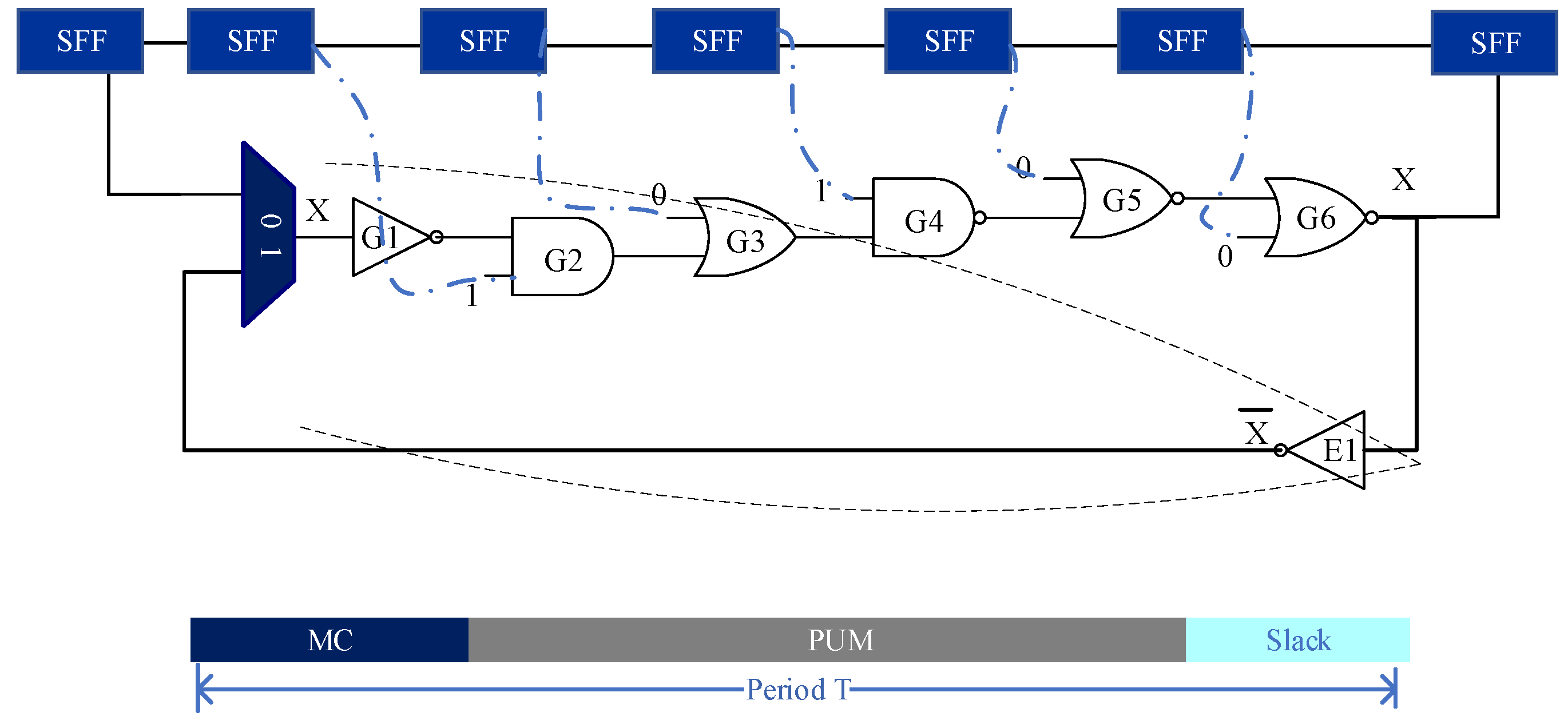
The basic concept of the conventional Path-RO measurement scheme uses critical paths and scan chains from the DFT of the circuit to construct a measurement structure, as shown in Figure 1. Critical paths are combinational logic paths between registers and/or memories that reflect timing changes in the device. The actual delay of the circuit can be accurately obtained by measuring the delay of the critical path.
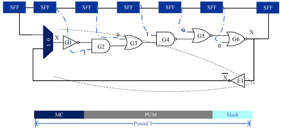
Figure 1.
The insertion-based Path-RO.
As the circuit is on standby (or during the manufacturing test), the shift-capture function of the DFT scan chain is multiplexed to punch the sensitization vectors into the critical path, thus configuring each cell in the critical path as an inverting device. A partial feedback logic control structure is then added to configure the critical path as an RO structure.
A schematic of the traditional Path-RO delay measurement method is shown in Figure 1. The DFT scan chains are used for path sensitization and some additional structures are added to the PUM for measurement control. The PUM can be configured as a Path-RO under the control of the oscillation signal (OE) and scan enable signal (SE) of the multiplexer (MUX).
The MUX controls the PUM operating in functional mode (0) and oscillation mode (1). In oscillation mode, the gates on the PUM must be set to noncontrolling values by sensitization patterns, which are obtained by commercial automatic test patterns generation (ATPG) tools.
The typical path delay test has three phases, the shift-in phase, the at-speed phase (for the launch and capture pulse), and the shift-out phase. The typical Path-RO scheme requires a measurement phase added after the shift-in phase. During the shift-in phase, the SE of the SFFs is enabled, and under the control of the shifting clock, the sensitization pattern for the PUM is shifted to the object SFFs. Then, the OE signal is enabled for path delay measurement. After the measure is completed, the counter output is stored in the system or shifted to ATE for processing.
The actual delay of the configured Path-RO can be obtained by using the relationship between the number of oscillations and the RO delay, as calculated in (1). There are errors in using DRO as a measurement result. These errors come from the measurement resolution and the additional MC circuit. The measurement resolution depends on the differences in oscillation frequency between two times of measurements, and the maximum resolution-dependent error is calculated by using (2) [19].
where DRO represents the delay of the entire RO loop, Tm is the measurement time, and Ncounter represents the number of transitions of the oscillating waveform during the measurement time.
2.3. Motivation
The basic Path-RO scheme is called insertion-based Path-RO in that paper because they need to insert a MUX into the PUM. However, the main problem of the insertion-based scheme is that the MUX inserted into the PUM leads to an increase in path delay, and finally increases the clock period of the original circuit, as shown in Figure 1. That is, it reduces the timing performance of the circuit.
To address the problem of performance loss and hardware overhead, we propose the BPath-RO architecture to minimize the impact on circuit performance with low hardware overhead.
3. BPath-RO Delay Measurement Scheme
This section describes the proposed BPath-RO scheme, including the controllability of the logic gate (Section 3.1), the configuration of BPath-RO for a single PUM (Section 3.2), the architecture (Section 3.3), and the calibration method (Section 3.4).
3.1. Controllability of the Logic Gates
The design of BPath-RO makes full use of the controllability of the logic gates in the test principle. In logic gates NAND and AND, if the signal on any input pin is 0, the output value of the gate will be fixed at 0 or 1, independent of the signals from the other pins. This type is known as the 0-control type (TYPE_0). Similarly, for logic gates such as NOR and OR, if any input signal is 1, the output value is independent of the other input signals, referred to as 1-control type (TYPE_1).
3.2. Configuration of Single PUM
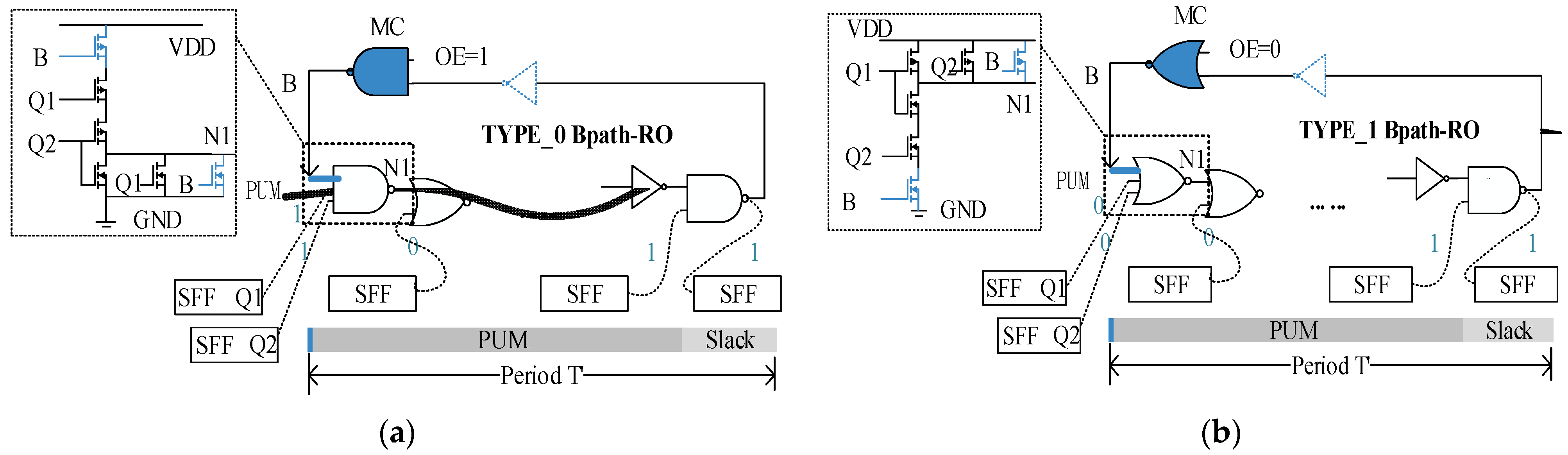
Two primary functions are to be implemented in BPath-RO: measurement and functional operation of the circuit. The main idea of BPath-RO is to establish a bypassed node by adding an input pin to the first gate of the PUM, thus allowing the measurement control structure (MC) to be placed on the return path instead of inserted into the PUM. The bypass-based design reduces the impact on the functional path delay. Figure 2 depicts two BPath-RO circuits with different controllability types for the first gate. The principle of bypass node creation and MC design is as follows.
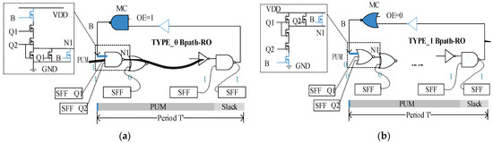
Figure 2.
Two types of BPath-RO with different types of first gates in PUM: (a) TYPE_0 BPath-RO; (b) TYPE_1 BPath-RO.
3.2.1. Bypass Node Creating
The dashed box in Figure 2a indicates the creation of the bypass node in the case where the first gate of the PUM is TYPE_0 (e.g., NAND2 in Figure 2). A bypass node B is added by simply adding a PMOS in parallel in the pull-up network and an NMOS in series in the pull-down network. The case of TYPE_1 PUM is similar and is shown in Figure 2b. The logic gate INV can be constructed as a two-input TYPE_0 or TYPE_1 logic gate (i.e., NAND2 or NOR2). For complex logic gates, such as heterodyne gates, a bypassed node can be constructed by inserting a TYPE_0 or TYPE_1 type two-input logic gate in front of it.
3.2.2. MC Design on Returning Path
The design of the MC depends on the control type of the first gate of the PUM. The control type of MC in the return loop is the same as that of the first gate in the PUM. For TYPE_0 PUM, it is recommended to use NAND2 as the control structure, as shown in Figure 2a. The two input pins of NAND2 are used as the oscillation enable (OE) (to control the transition between measurement and operation modes) and the return line of the PUM output, respectively. For the first PUM with gate type TYPE_1, NOR2 serves as the control structure. In addition, the MC acts as an inverter in the measurement mode, and the BPath-RO configuration requires an odd number of reversing structures. If the number of reversing units in the PUM is odd, an additional reverser is needed at the end of the PUM on the feedback path.
During operation mode, the created bypassed node is set to a non-control value to ensure the normal operation function of PUM when the MC is bypassed with minimal effect on the PUM’s delay. Conversely, in measurement mode, the MC transmits the output signals of the PUM to the bypassed node, thus reconfiguring the PUM to RO and enabling in situ measurement of the PUM. BPath-RO requires only two transistors inserted into the PUM, and the bypass-based design has almost negligible impact on functional path delay, making it a performance- and area-efficient design.
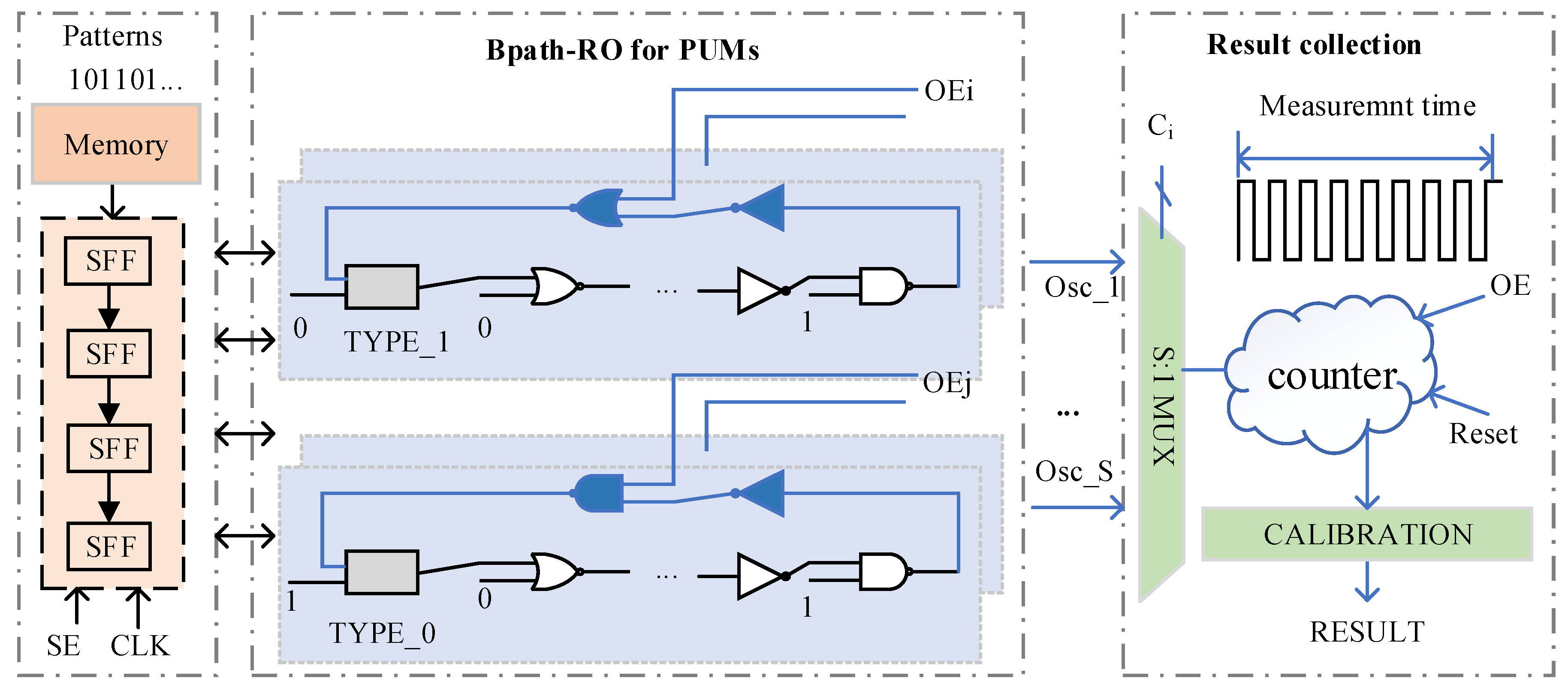
3.3. Architecture of BPath-RO
The BPath-RO architecture is shown in Figure 3. Patterns for path sensitization are generated and pre-stored in the on-chip memory. The PUM is sensitized by reusing the scan chain of DFT. A resettable counter is utilized to collect the number of oscillations of the BPath-RO throughout the measurement period. The counter is synchronized with the oscillation enable signal (OE) to ensure precise and accurate counting. A shared controller in the form of an S:1 MUX with Ci is utilized to timeshare the counter among the PUMs. The measurement count results are processed using a software-based calibration unit.
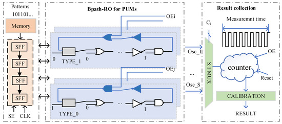
Figure 3.
The architecture of BPath-RO.
There are three modes of the circuit: operation, scan, and measurement, as shown in Table 1. (1) Switching from operation mode to scan mode: the SE is set to the enabled value, and the path sensitization patterns are scanned and propagated to the nodes of the object PUM for path sensitization. (2) Switching from scan mode to measurement mode: the SE is set to unable, and the OE is assigned to non-control values to activate BPath-RO and start the oscillation measurement. (3) Switching from measurement mode to operation mode: the OE is assigned to the corresponding control value.

Table 1.
Signal assignment for mode switching.
3.4. Software-Based Calibration
In the proposed BPath-RO scheme, the delay of the MC is included in the measurement results and must be calibrated. Since the MC structure is small and can be placed in the same physical space as the PUM through an engineering change order (ECO), the PVT rate of change for the MC is the same as the PUM.
In the design phase, the delays of the MC and RO under various PVT and aging effect conditions can be obtained using a Monte Carlo simulation. Then, the calibration parameters (RMC) are calculated statistically and stored on the chip for field measurement calibration. The RMC is calculated as (3) and (4):
where DMC(i) and DRO(i) represent the responding delay of the MC to the BPath-RO at the ith variation, and RMC(i) is the ratio. RMC takes the mean value of RMC(i) under M variations.
After the field measurements, the delay DRO of the BPath-RO is first obtained using (1). Then, the delay of the PUM DPUM is derived from the above calibration parameters RMC as in (5).
4. Results
In this section, the proposed BPath-RO is validated in terms of measurement accuracy, impact on the performance of the original circuit, and hardware area overhead. In addition, it is compared and analyzed with the conventional insertion-based Path-RO in these three aspects. In the comparison experiments, the extra features in the insertion-based schemes, i.e., the self-enabling features in [18], are removed for fairness.
To account for the effect of the path length on the measurement performance, the measurement structures were implemented on ISCAS’89 s298 and ITC’99 b15. Circuit s298 is a traffic signal controller circuit containing 119 logic gates and 14 flip-flops, which serves as a representative of the short-path circuits. Circuit b15 is an 80386 processor (subset) containing 8367 gates and 449 flip-flops and is representative of a long-path circuit. The details of the PUMs are shown in Table 2. According to the representative path selection method in the literature [19], two PUMs from s298 were selected as short path representatives, and six PUMs from b15 were selected as large path representatives. The normal delays of the paths were obtained using the Synopsys Hspice 2021 tool. The operating conditions were the typical 45 nm process, voltage = 1.1 V, temperature = 25 °C, transition time = 40 ps, and fresh time. The last column indicates the first gate of the PUM and the parity of the PUM, respectively.
Table 2.
Basic information on the selected PUMs.
4.1. Analysis of Accuracy
To verify the measurement accuracy of the proposed scheme, we simulated the delay of the PUMs in Table 2 under different variation conditions, and the detailed PVTA conditions are shown in Table 3.
Table 3.
Variations are considered in the simulation.
After adding the measurement structure to the PUM, we obtained the new PUM (PUM’). The actual delay (gold value) of the PUM’ was the simulated value of the propagation delay between the inputs and outputs of the path in the operating mode, using the Hspice command. The measured delay was the calculated result of the counter result in the measurement mode using the oscillating waveform as the counter clock, according to (1) and calibrated by the calibration coefficients RMC obtained by (5) as detailed in Section 3.4.
The measurement errors under different simulation conditions are shown in (6), where Dactual_i and Dmeas_i are the simulation delay and the measurement delay of the PUM’ under the ith variation.
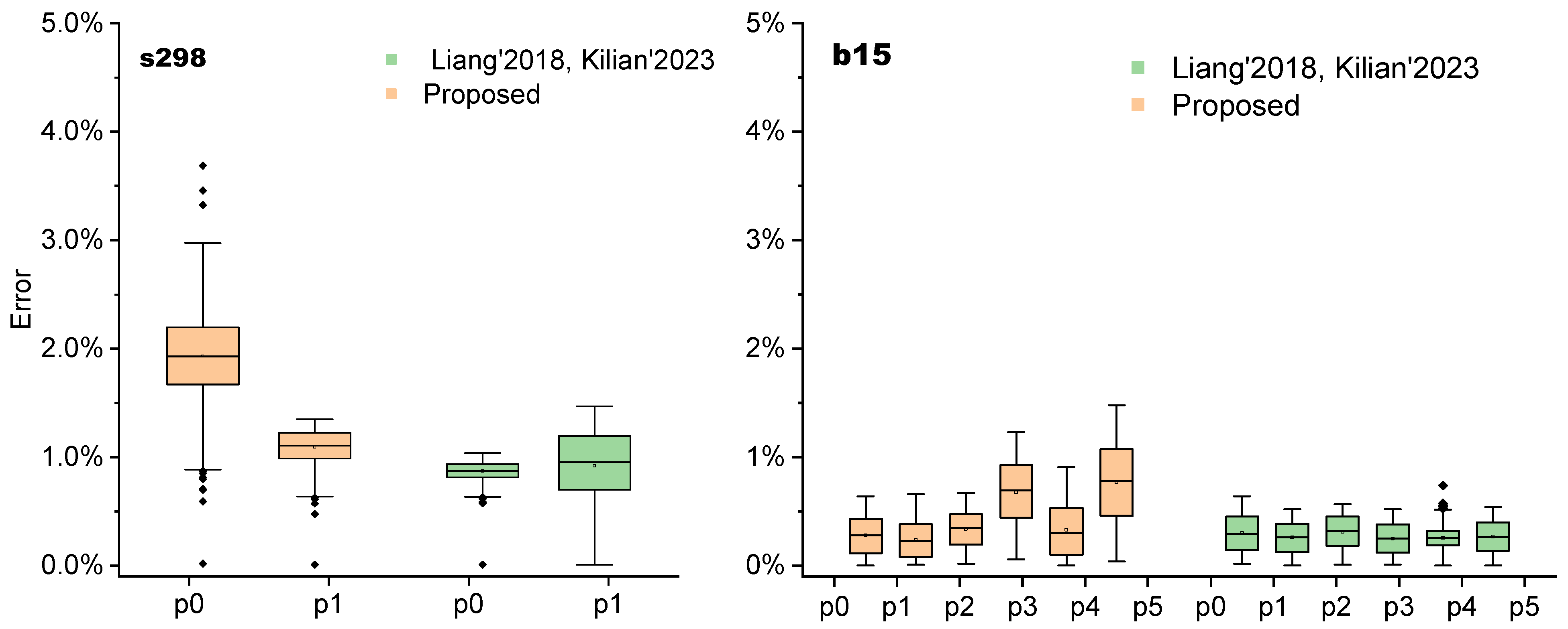
Figure 4 shows the measurement results for some of the critical paths in the representative circuits s298 for short paths and b15 for long paths, where the statistics of the maximum, minimum, and average measurement error Error_i under different PVTA variations are described.
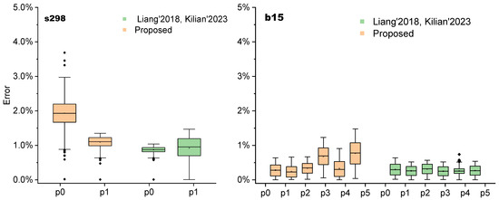
Figure 4.
Error comparison with the insertion-based structures in Liang’2018 [19] and Kilian’2023 [23].
For a fair comparison, we simplified the measurement structure of the insertion type [19,23], i.e., only the main measurement structure that uses a multiplexer for the Path-RO configuration in the measurement structure was retained. It can be seen that the overall measurement errors of the representative circuit s298 for short paths were relatively high but not higher than 4%. The measurement errors of b15 were small overall, with none of the errors exceeding 2%. The relatively small measurement error for the long path was because the delay of the measurement structure was a much smaller percentage of the delay of the path to be measured. Comparing the error data between the structure of this paper and the inserted structure, the method of this paper had a smaller measurement error relative to the inserted method because we added the process of data calibration.
4.2. Analysis of Timing Performance Impact
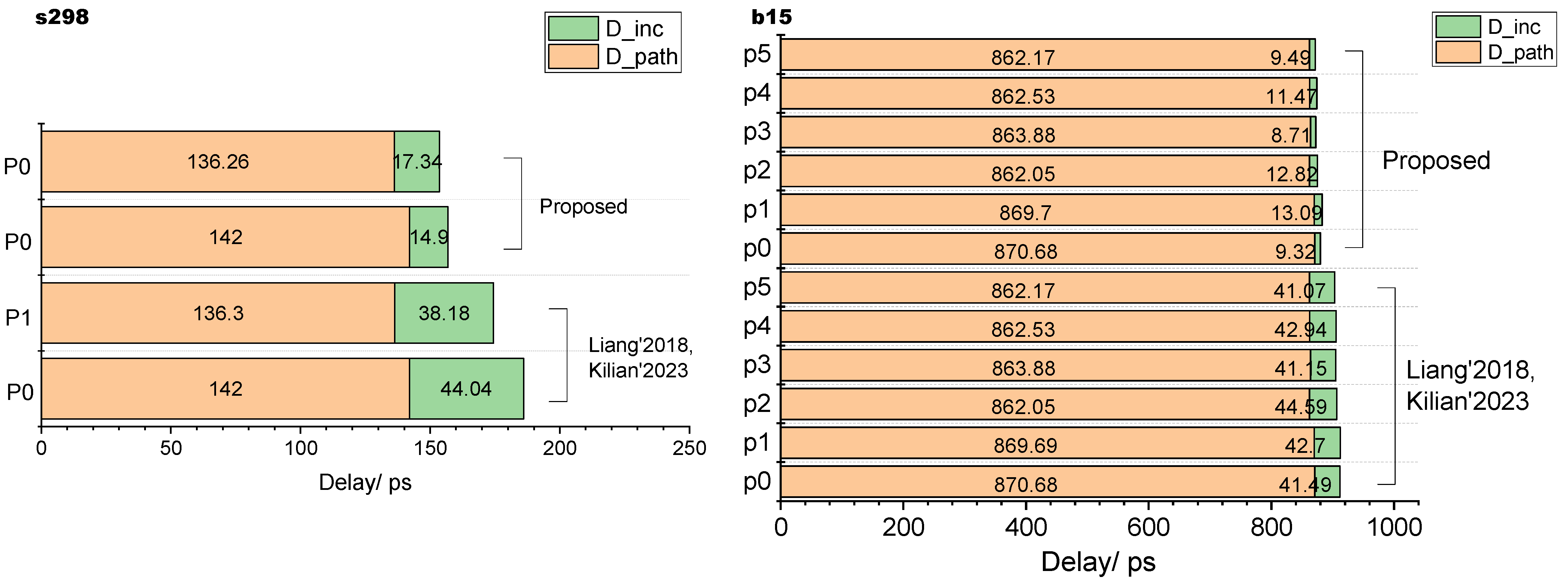
The impact on the circuit performance was assessed in terms of the change in the critical path delay before and after the introduction of the measurement structure. The insertion-based Path-ROs insert the MC directly into the PUM, significantly impacting circuit performance. Alternatively, the proposed BPath-RO only adds two transistors to the PUM, and the MC is placed in the bypass.
As shown in Figure 5, two critical paths of s298 {P0, P1} and six critical paths of b15 {P0, P1, P2, P3, P4, P5} were configured to the Bpath-RO and the inserted Path-RO for comparison. The path delays were simulated under a typical 45 nm process node, voltage = 1.1 V, temperature = 25 °C, at fresh time. D_path is the delay of the critical path. D_inc is the increased delay after configuring to the RO owing to the MC structures. The total delay is the critical path delay after configuring to the RO, which may impact the circuit performance. As we can see, this is because the MUX is inserted into the object path, and we just added two transistors to the object path.

Figure 5.
Comparison of delay increases with the insertion-based methods in Liang’2018 [19] and Kilian’2023 [23].
The delay increment of the insertion-based Path-ROs [19,23] varied between 38.18 ps and 44.59 ps, which was affected by path parity, such as with P0 and P1 of the s298, where P0 has an even number of inverter-type devices, which needs one more inverter for configuration, while P1 has an odd number of inverter devices. The delay increment of the proposed method varied between 8.71 ps and 17.34 ps, which was because the MC structure depends on the first gate of the critical path.
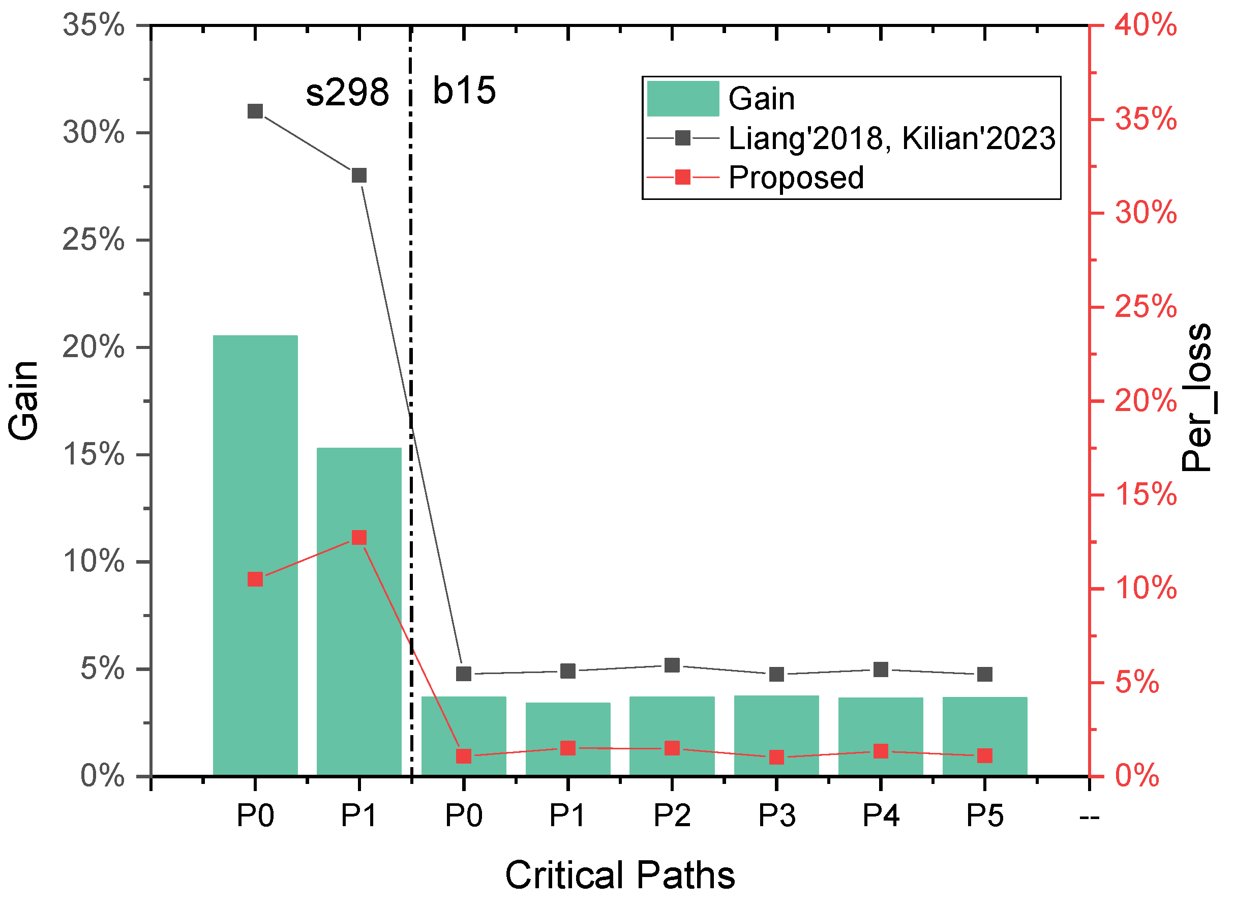
Path delay increase has an impact on performance. To evaluate the effectiveness of our scheme, the performance loss Ploss was computed using (7). The circuit performance gain Gain from using BPath-ROs over the insertion-based Path-ROs was calculated as (8).
where DBPath-RO and Dinsert represent the path delay after constructing the BPath-RO and the insertion-based Path-RO, respectively.
As shown in Figure 6, using the insertion-based measurement method, the incremental path delay caused by building a Path-RO measurement structure for the critical paths {P0, P1} in s298 was 30.1% and 28.02%, with an average of 29.52%, while b15 had an average of 4.89% incremental path delay. Using the BPath-ROs measurements proposed in this paper, the incremental path delays induced by building the measurement structures for {P0, P1} in s298 were 10.49% and 12.72%, with an average of 11.61%, while the average incremental delay for b15 was 1.25%.
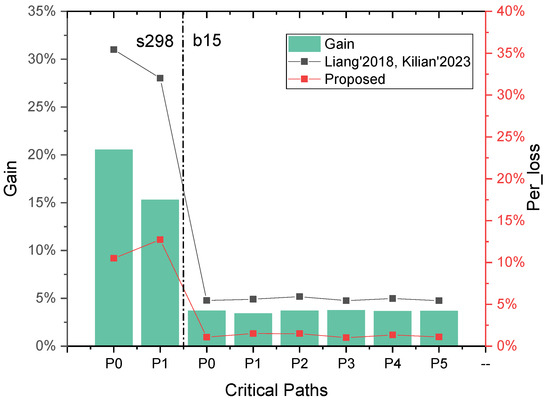
Figure 6.
Comparison of performance impact with the insertion-based methods in Liang’2018 [19] and Kilian’2023 [23].
In comparison, the performance overhead of the BPath-RO in this paper was improved by an average of 13.81% (s298) and 3.47% (b15) over the insertion-based Path-RO.
4.3. Analysis of Hardware Overhead
The overall hardware overhead consists of the hardware of the MC in each PUM and the shared part for result collection.
For the shared part, a MUX and a counter are mainly required. The resolution determines the scale of the counter. Take circuit b15, for example; the path delay is about 1 ns and even more in the worst case, and a 12-bit counter is required to meet the resolution. The size of the shared MUX is determined by the number of PUMs, i.e., measuring 16 PUMs requires a 16:1 MUX, and typically, larger MUXs (over eight inputs) consist of smaller MUXs arranged in a tree manner. Therefore, as the number of PUMs increases, the overall hardware overhead increases further. Reducing the hardware overhead should be improved in terms of reducing the number of PUMs. Our architecture does not differ from the existing architecture in the shared part; therefore, comparisons were not made.
For a single PUM, the magnitude of the hardware overhead affects the implementation of ECO and, therefore, needs to be focused on. In the case of the insertion-based Path-ROs, they require a MUX inserted into the PUM, which requires 20 transistors. The proposed BPath-RO scheme only added a bypassed node to the first gate of the PUM, with either a NAND2 or a NOR2 performed as the MC on bypass, which requires 2 transistors inserted in paths and 4~6 transistors on the bypass. Therefore, the hardware overhead of the proposed BPath-RO on a single path can be reduced by 60~70%.
5. Conclusion and Outlook
In this paper, a novel delay measurement scheme, BPath-RO, was proposed, which utilizes a bypass-based RO construction manner. The measurement accuracy of BPath-RO is comparable to the existing insertion-based scheme when measuring circuit paths of different lengths. The proposed BPath-RO reduces the critical path performance loss by 13.81% in s298 and 3.47% in b15. In addition, the hardware cost of a single PUM is reduced by 60%.
Future work will focus on optimizing the path selection process based on [21,25] to improve measurement efficiency. In addition, a reduction in measurement time is critical for resilience and manufacturing screening applications, and future work will design parallel measurement schemes in terms of a reduction in measurement time.
Author Contributions
D.L.: conceptualization, data curation, investigation, methodology, visualization, and writing—original draft, review, and editing. H.L.: conceptualization, formal analysis, funding acquisition, and writing—review and editing. H.Z. and Y.W.: resources, software, data curation, and investigation. Y.L., M.Y. and Z.H.: formal analysis. All authors have read and agreed to the published version of the manuscript.
Funding
This work was supported in part by the National Natural Science Foundation of China (NSFC) under Grant 62027815, Grant 61834006, Grant 62274052, Grant 61874156, and Grant 61904001.
Data Availability Statement
The data presented in this study are available in the article.
Acknowledgments
The authors thank the editor and anonymous referees for their helpful comments for improving the quality of this paper.
Conflicts of Interest
The authors declare no conflict of interest.
References
- Hill, I.; Chanawala, P.; Singh, R.; Sheikholeslam, S.A.; Ivanov, A. CMOS Reliability From Past to Future: A Survey of Requirements, Trends, and Prediction Methods. IEEE Trans. Device Mater. Reliab. 2022, 22, 1–18. [Google Scholar] [CrossRef]
- Kumar, S.V.; Kim, C.H.; Sapatnekar, S.S. Adaptive Techniques for Overcoming Performance Degradation Due to Aging in CMOS Circuits. IEEE Trans. Very Large Scale Integr. (VLSI) Syst. 2011, 19, 603–614. [Google Scholar] [CrossRef]
- Heo, J.; Jeong, K.; Choi, J.Y.; Kim, T.; Choi, K. Hardware Performance Monitoring Methodology at Near-Threshold Computing and Advanced Technology Nodes: From Design to Postsilicon. IEEE Trans. Comput-Aided Des. Integr. Circuits Syst. 2022, 41, 1929–1942. [Google Scholar] [CrossRef]
- Cantoro, R.; Huch, M.; Kilian, T.; Martone, R.; Schlichtmann, U.; Squillero, G. Machine learning based performance prediction of microcontrollers using speed monitors. In Proceedings of the IEEE International Test Conference (ITC), Washington, DC, USA, 1–6 November 2020. [Google Scholar]
- Bernardi, P.; Restifo, M.; Reorda, M.S.; Appello, D.; Bertani, C.; Petrali, D. Applicative system level test introduction to increase confidence on screening quality. In Proceedings of the 23rd International Symposium on Design and Diagnostics of Electronic Circuits & Systems (DDECS), Novi Sad, Serbia, 22–24 April 2020. [Google Scholar]
- Polian, I.; Anders, J.; Becker, S.; Bernardi, P.; Chakrabarty, K.; ElHamawy, N.; Sauer, M.; Singh, A.; Reorda, M.S.; Wagner, S. Exploring the mysteries of system-level test. In Proceedings of the IEEE 29th Asian Test Symposium (ATS), Penang, Malaysia, 23–26 November 2020. [Google Scholar]
- Mu, S.P.; Chao, M.C.T.; Chen, S.H.; Wang, Y.M. Statistical Framework and Built-In Self-Speed-Binning System for Speed Binning Using On-Chip Ring Oscillators. IEEE Trans. Very Large Scale Integr. (VLSI) Syst. 2016, 24, 1675–1687. [Google Scholar] [CrossRef]
- Zhang, T.T.; Gao, Y.K.; Walker, D.M.H. Pattern Generation for Post-Silicon Timing Validation Considering Power Supply Noise. In Proceedings of the North Atlantic Test Workshop (NATW), Johnson City, NY, USA, 14–16 May 2014. [Google Scholar]
- Labbe; Fan, P.; Achuthan, T.; Prabhat, P.; Knight, G.P.; Myers, J. A Supply Voltage Control Method for Performance Guaranteed Ultra-Low-Power Microcontroller. IEEE J. Solid-State Circuits 2021, 56, 601–611. [Google Scholar] [CrossRef]
- Masuda, Y.; Hashimoto, M. MTTF-Aware Design Methodology of Adaptively Voltage Scaled Circuit with Timing Error Predictive Flip-Flop. IEICE Trans. Fundam. Electron. Commun. Comput. Sci. 2019, E102A, 867–877. [Google Scholar] [CrossRef]
- Okuhara, H.; Ahmed, A.B.; Amano, H. Digitally Assisted On-Chip Body Bias Tuning Scheme for Ultra Low-Power VLSI Systems. IEEE Trans. Circuits Syst. I-Regul. Pap. 2018, 65, 3241–3254. [Google Scholar] [CrossRef]
- Sadi, M.; Kannan, S.; Winemberg, L.; Tehranipoor, M. SoC speed binning using machine learning and on-chip slack sensors. IEEE Trans. Comput.-Aided Design Integr. Circuits Syst. 2017, 36, 842–854. [Google Scholar] [CrossRef]
- Heo, J.; Jeong, K.; Kim, T.; Choi, K. Synthesis of hardware performance monitoring and prediction flow adapting to near-threshold computing and advanced process nodes. In Proceedings of the 25th Asia and South Pacific Design Automation Conference (ASP-DAC), Beijing, China, 13–16 January 2020. [Google Scholar]
- Sai, G.; Halak, B.; Zwolinski, M. Multi-Path Aging Sensor for Cost-Efficient Delay Fault Prediction. IEEE Trans. Circuits Syst. II-Express Briefs 2018, 65, 491–495. [Google Scholar] [CrossRef]
- Jung, J.; Ansari, M.A.; Kim, D.; Yi, H.; Park, S. On Diagnosing the Aging Level of Automotive Semiconductor Devices. IEEE Trans. Circuits Syst. II-Express Briefs 2018, 64, 822–826. [Google Scholar] [CrossRef]
- Paul, S.; Krishnamurthy, S.; Mahmoodi, H.; Bhunia, S. Low-overhead design technique for calibration of maximum frequency at multiple operating points. In Proceedings of the IEEE/ACM International Conference on Computer-Aided Design (ICCAD), San Jose, CA, USA, 4–8 November 2007. [Google Scholar]
- Xiaoxiao, W.; Tehranipoor, M.; Datta, R. Path-RO: A novel on-chip critical path delay measurement under process variations. In Proceedings of the IEEE/ACM International Conference on Computer-Aided Design (ICCAD), San Jose, CA, USA, 10–13 November 2008. [Google Scholar]
- Wang, X.; Tehranipoor, M.; George, S.; Tran, D.; Winemberg, L. Design and Analysis of a Delay Sensor Applicable to Process/Environmental Variations and Aging Measurements. IEEE Trans. Very Large Scale Integr. (VLSI) Syst. 2012, 20, 1405–1418. [Google Scholar] [CrossRef]
- Liang, H.; Fang, X.; Yi, M.; Huang, Z.; Lu, Y. A novel BIST scheme for circuit aging measurement of aerospace chips. Chin. J. Aeronaut. 2018, 31, 1594–1601. [Google Scholar] [CrossRef]
- Sakellariou, P.; Paliouras, V. Reconfigurable RO-Path Delay Sensor. IEEE Trans. Circuits Syst. II-Express Briefs 2018, 65, 2027–2031. [Google Scholar] [CrossRef]
- Kilian, T.; Ahrens, H.; Tille, D.; Huch, M.; Schlichtmann, U. A Scalable Design Flow for Performance Monitors Using Functional Path Ring Oscillators. In Proceedings of the IEEE International Test Conference (ITC), Anaheim, CA, USA, 10–15 October 2021. [Google Scholar]
- Kilian, T.; Hanel, M.; Tille, D.; Huch, M.; Schlichtmann, U. Reducing Routing Overhead by Self-Enabling Functional Path Ring Oscillators. In Proceedings of the IEEE European Test Symposium (ETS), Barcelona, Spain, 23–27 May 2022. [Google Scholar]
- Kilian, T.; Tille, D.; Huch, M.; Hanel, M.; Schlichtmann, U. Performance Screening Using Functional Path Ring Oscillators. IEEE Trans. Very Large Scale Integr. (VLSI) Syst. 2023, 31, 711–724. [Google Scholar] [CrossRef]
- Firouzi, F.; Ye, F.; Chakrabarty, K.; Tahoori, M.B. Aging- and Variation-Aware Delay Monitoring Using Representative Critical Path Selection. ACM Trans. Des. Autom. Electron. Syst. (TODAES) 2015, 20, 1–23. [Google Scholar] [CrossRef]
- Hu, Y.; Ye, J.; Shi, Z.; Li, X. LAPS: Layout-aware path selection for post-silicon timing characterization. IEICE Trans. Inf. Syst. 2017, 100, 323–331. [Google Scholar] [CrossRef]
- Jiang, J.-H.R.; Kravets, V.N.; Lee, N.-Z. Engineering Change Order for Combinational and Sequential Design Rectification. In Proceedings of the Design, Automation & Test in Europe Conference & Exhibition (DATE), Grenoble, France, 9–13 March 2020. [Google Scholar]
Disclaimer/Publisher’s Note: The statements, opinions and data contained in all publications are solely those of the individual author(s) and contributor(s) and not of MDPI and/or the editor(s). MDPI and/or the editor(s) disclaim responsibility for any injury to people or property resulting from any ideas, methods, instructions or products referred to in the content. |
© 2023 by the authors. Licensee MDPI, Basel, Switzerland. This article is an open access article distributed under the terms and conditions of the Creative Commons Attribution (CC BY) license (https://creativecommons.org/licenses/by/4.0/).