1. Introduction
One of the rapidly advancing fields in the era of the Fourth Industrial Revolution is wearable devices. Wearable devices need to be easy to attach to the body and portable, so miniaturization and low-power operation are essential. The bioelectrical signals processed by wearable devices are characterized by small amplitude and low frequency, and the amplitude and frequency range of each signal (ECG, EMG, EEG, and EOG) are different [
1]. If an ADC is designed specifically for each characteristic of the bioelectrical signals, there may be a problem of power consumption to be wasted and chip area being increased more than it is required. For example, if a high-resolution ADC such as 14 bits or more are utilized to process low-resolution signals, the employment of high-resolution ADC results in large power consumption. In this case, an ADC with resolution reconfigurable circuitry is employed on a single chip, which can contribute to the miniaturization and low-power operation of wearable devices.
ADCs with reconfigurable architectures have been implemented in various ways. Liu [
2] adopted a structure that can reconfigure 1-bit/cycle and 2-bit/cycle, and Shen [
3] designed an ADC that was reconfigured as a Time-interleaving SAR ADC with 1–4 channels, allowing reconfigurable resolution and speed. Yip [
4] not only allows resolution reconfiguration from 5 to 10 bits but also enables power consumption reconfiguration by adjusting the supply voltage from 0.4 V to 1 V. However, [
2,
3,
4] are all designed with a structure that reconfigures the capacitor DAC (C-DAC) of the SAR ADC, making high-resolution design impossible. Refs. [
2,
3] also showed high-speed operation, resulting in high power consumption and being unsuitable for bio-signal processing.
Refs. [
5,
6] implemented 12-bit ADCs based on the conventional single-step/two-step SAR architecture without reconfigurability to handle various bio-signals. Recently, hybrid ADCs that employ two or more different ADC structures have been widely designed to take advantages of strength of each structure. Among those, the pipeline-SAR ADC [
7], which combines a pipeline ADC and a SAR ADC, achieved a sampling rate of 38 GS/s using a dynamic residue amplifier with a Time-interleaving (TI) structure, but it consumed a large power of 37 mW per channel. Due to large power consumption, Ref. [
7] would be suitable for image signal processing. On the other hand, the noise-shaping SAR ADC [
8,
9,
10], which combined the SAR ADC and ΔΣ modulator, showed a low sampling rate of 10 kS/s, 1.6 MS/s, and 3.7 MS/s, and Refs. [
9,
10] achieved a high effective number of bits (ENOB) 11.7 and 12.6 bits, respectively. However, Ref. [
9] and Ref. [
10] exhibit a relatively large power consumption of 60 μW and 150 μW, respectively, due to the power consumption of the operational amplifier.
Furthermore, the SAR-SS ADC, which combined the SAR and the single-slope architecture, can obtain both the low power consumption of the SAR ADC and the high linearity of the single-slope ADC, making it suitable for bio-signal processing. Among the previously designed SAR-SS ADCs, Kwon [
11] implemented SAR-SS ADC that employed an operational amplifier to generate a ramp voltage with resistor ladder, resulting in a power consumption of 56 μW, and Figure of Merit (FoM) of 36.9 fJ/step. Liu [
12] achieved a low FoM of 2.2 fJ/step by sharing the circuit between the SAR ADC and a digital single-slope ADC, but the structure is complex due to the decoder circuit that converts the thermometer code into a binary code, and the power consumption is high at 350 μW due to the high speed of 100 MS/s. Additionally, a Level-crossing (LC) architecture has been designed that combines the single slope ADC and ΔΣ modulator, and LC-SAR hybrid ADC [
13] exists that combines the LC ADC and SAR ADC. However, Ref. [
13] shows high power consumption of 205 μW because of the ΔΣ modulator, and its ENOB is 8.59-bit, which is not high enough. Zhao [
14] designed the 10-bit SAR ADC with single-ended structure to achieve an extreme low power consumption of 94-nW and ENOB of 9.3-bit.
In this paper, we propose a reconfigurable SAR-SS hybrid ADC that achieves a low sampling rate and low power consumption suitable for processing bioelectrical signals, while being able to process various bio-signals on a single chip. The proposed ADC employs resolution reconfiguration through external input signals and is implemented using a single-slope bit shifting method that reconfigures only the digital blocks of the circuit. Section II explains the design methodology of the proposed ADC, and Section III describes the structure and operation of the proposed ADC. Section IV presents the experimental results, and Section V concludes the paper.
2. Proposed Architectures
Figure 1 shows the overall block diagram of the proposed fully differential reconfigurable SAR-SS hybrid ADC. The proposed circuit consists of an SAR ADC allowing resolution reconfiguration from 8 to 10 bits, and a 4-bit Single-slope ADC. It includes a 14-bit C-DAC with switch array for control, a reconfigurable SAR logic, a digital ramp generator for single-slope ramp signal generation, a comparator with a double-tailed structure, a reset signal generator for ADC initialization, and an output register that processes the overall conversion result and converts it into the final output bit signal. To reduce the overall capacitance and layout area, the 14-bit C-DAC uses split capacitor (C
S = 128/127C
U). Conventional SAR ADC has a structure that the digital output signal from the SAR logic applies to the C-DAC. However, in the circuit of
Figure 1, the SAR logic is only connected to the upper 10 bits of the C-DAC, while the lower 6 bits are connected to the single-slope digital ramp generator, which applies a 4-bit binary signal. Each block contains an external resolution control signal
C1C0 composed of 2 bits, allowing resolution reconfiguration from 12 to 14 bits.
The single-slope digital ramp generator connected to the C-DAC generates a ramp signal that increases by 1 LSB per step from the remaining residual voltage after the conversion of the SAR ADC connected for the upper bits is completed. Since the C-DAC and the single-slope digital ramp generator are connected differentially to the inputs of the comparator, the ramp signal appears as two symmetrical signals centered around the common mode voltage (VCM). The binary codes from the SAR logic and the single-slope digital ramp generator are input to the output register and synchronized with the reset signal, resulting in the final digital code output.
The timing diagram of the proposed circuit is shown in
Figure 2. The reset generator produces two reset signals, RESET
SAR and RESET
SS. First, the RESET
SAR signal performs the role of initializing the entire ADC for one clock cycle, while the RESET
SS signal drives the single-slope digital ramp generator during the next 16 clock cycles after the SAR ADC conversion is completed. While the RESET
SS signal is in a low state, the single-slope digital ramp generator produces the 4-bit binary code from ‘0000’ to ‘1111’ which is received by the C-DAC to generate the ramp voltage to the input terminal of the comparator, COMP_IN+ and COMP_IN−.
The proposed circuit allows the reconfigurable circuit to utilize the single-slope bit shifting method. The 12-bit mode, 13-bit mode, and 14-bit mode circuit diagram are presented in
Figure 3,
Figure 4 and
Figure 5, respectively.
Unlike the conventional structure, the proposed circuit offers functionality to vary resolution in the SAR Logic. As an n-bit SAR Logic is connected to the C-DAC control switch array, the 4-bit single-slope ramp generator should be connected to the (n − 1)th to (n − 4)th bit of the C-DAC.
First, when
C1C0 = 00
(2), the resolution of the SAR logic becomes 8-bit. At this time,
D5 and
D4 are connected to
Q5 (
B3) and
Q4 (
B2) of the single-slope Ramp generator, as shown in
Figure 3, and the 4-bit output binary codes from the single-slope ramp generator are applied to the upper 9th bit to 12th bit such as
B3,
B2,
B1,
B0, respectively. Therefore, in case of
C1C0 = 00
(2), the entire ADC is functional with the resolution of 12-bit which includes 8-bit (SAR) and 4-bit (single slope). Secondly, when
C1C0 = 10
(2),
D5 is connected to
S1 of the SAR logic, as illustrated in
Figure 4, and
B3,
B2,
B1, B0 are connected to
Q4,
Q3,
Q2,
Q1 of the single-slope ramp generator, respectively. In case of
C1C0 = 10
(2), the entire ADC is functional with the resolution of 13-bit which includes 9-bit (SAR) and 4-bit (single slope). Lastly, when
C1C0 = 11
(2),
D4 and
D5 are connected to
S0 and
S1 of the SAR logic, as shown in
Figure 5, and
B3,
B2,
B1,
B0 are connected to
Q3, Q2,
Q1,
Q0 of the single-slope ramp generator, respectively. In case of
C1C0 = 11
(2), the entire ADC is functional with the resolution of 14-bit which includes 10-bit (SAR) and 4-bit (single slope). And when
C1C0 = 01
(2), there is no assigned resolution, so the reconfigurable reset generator is made to not generate RESET
SAR and RESET
SS signals, hence all output digital codes are generated as 0. Reconfigurable ADC operation based on the bit shifting method is summarized in
Table 1.
LSB and LSB-1 of the SAR logic are
S0 and
S1, and the 4-bit binary output signals of the 4-bit single slope ramp generator are denoted as
B3,
B2,
B1,
B0 from the MSB to the LSB. Boolean expressions for
D4 and
D5 are represented as follows:
The output stage of the single-slope digital ramp generator produces a total of six outputs. Depending on the reconfigured resolution, four outputs out of the six ones are selected to generate a 4-bit binary signal. Considering the six outputs as
Q5, Q4, ⋯, Q0 from the MSB to the LSB, the resolution of the
n-bit SAR Logic (
n = 8~10) is determined by the
C1 and
C0 signals. The bits (
B3B2B1B0) are connected to the six output terminals, as shown in
Table 2, by performing bit shift operation from the (
n − 1)th bit to the LSB. In the 13-bit mode, the LSB part (
Q0) of the 14-bit C-DAC is set to ground, resulting in the 14th bit always to become a “0” code. Similarly, in the 12-bit mode, the 13th bit (
Q1) and 14th bit (
Q0) become as “0” code.
In the process of reconfiguring the resolution, the overall ADC possesses nonlinearity due to the split capacitor of the 14-bit C-DAC. To increase linearity, it is desirable to set the resolution of the single-slope ADC as large as possible to minimize the nonlinearity caused by the split capacitor. However, as the resolution of the single-slope ADC increases, the sampling period of the entire ADC increases exponentially, resulting in a drawback of decreasing data conversion speed of ADC. Hence, to increase the sampling speed while preventing degradation of linearity, it is necessary to distribute the resolution of the SAR ADC and single-slope ADC appropriately.
If the resolution of the SAR ADC and the single-slope ADC are denoted as
M bit and
N bit, respectively, the total resolution,
Rtotal is given by
Additionally, the data conversion time,
Tconv of the proposed ADC is described as follows:
where
Tclk is the clock period. The total sampling period,
Ttotal, is calculated by adding one clock for input signal sampling and another clock for data output to (4), resulting in the following expression:
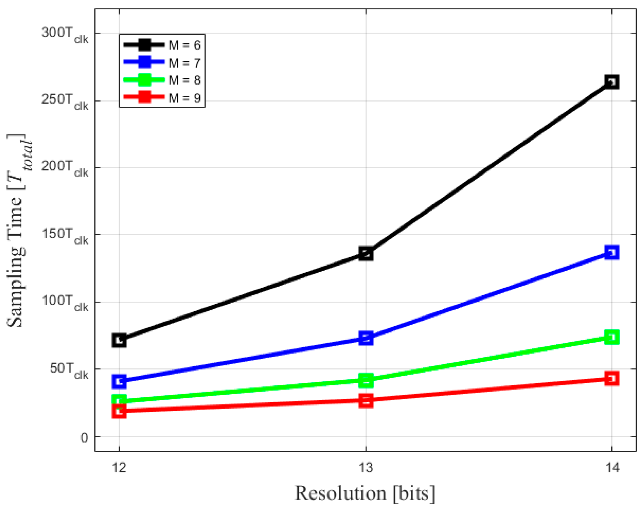
Figure 6 presents
Ttotal as a function of total bit of ADC with different four resolutions of SAR, namely,
M = 6, 7, 8, 9. As M increases,
Ttotal also increases linearly according to (5).
Figure 7 illustrates
Ttotal as a function of total bit of ADC with different four resolutions of single-slope ADC, namely,
N = 3, 4, 5, 6.
Ttotal increases as N increases.
It can be seen from
Figure 6 that as the resolution increases from 12-bit to 14-bit with
M fixed, sampling time increases exponentially. In contrast,
Figure 7 shows that the sampling time increases linearly as a function of resolution. In other words, by reconfiguring the resolution of the SAR ADC and keeping the resolution of the single-slope ADC fixed, the sampling time changes only by one
Tclk, allowing the sampling speed to remain relatively constant.
On the other hand, when
N becomes less than 4, the maximum value of
Ttotal according to (5) is 28
Tclk. In this case, the reset generator produces the RESET
SAR signal with a period of 28
Tclk, which can be implemented using a binary counter with 5 J-K flip-flops. However, when
N becomes greater than 4,
Ttotal becomes greater than 32
Tclk, leading to large power consumption. To avoid this situation, the proposed hybrid ADC adopted the resolution of the single-slope ADC to be fixed to 4-bit and reconfigurable resolution (8 to 10-bit) of SAR ADC. The linearity of SS-ADC (single-slope ADC) is generally proportional to the resolution of SS-ADC. However, as the resolution (
N) of SS-ADC increases, the number of clocks required for data conversion increases by
time. Since the resolution to process the bio-signal requires up to 12-bit, the 14-bit resolution is chosen for the proposed work, so that SAR ADC and SS-ADC cover 10-bit and 4-bit, respectively. As the resolution of SS-ADC increases more than 4-bit, the number of D flip-flop within the reconfigurable reset generator increases and results in increasing chip area and power consumption. Since total capacitance of 10-bit DAC in the proposed work is capable of handling the maximum bandwidth (20 kHz) of ExG signal (all bio-signals) [
1], the proposed work chose 10-bit C-DAC for SAR and 4-bit for single-slope ADC with reconfigurability.
3. Circuit Implementation
The circuit diagram of the reconfigurable SAR Logic shown in
Figure 1 is implemented in
Figure 8.
The circuit shown in
Figure 8 consists of a total of 10-bit shift registers and SAR control logic using D flip-flops. Among the D flip-flops, there are six switches connected, allowing the circuit structure to be reconfigured to operate as 8 to 10 bits depending on the
C1 and
C0 signals. The six switches are controlled by the signals
SW1 and
SW2, which can be expressed as (6) and (7), respectively.
According to (6) and (7), the resolution of the reconfigurable SAR Logic varies as presented in
Table 3.
The circuit diagram of the single-slope digital ramp generator is presented in
Figure 9. The circuit is composed of a 4-bit binary counter and a multiplexer array containing six multiplexers. Four bit (
Q0,
Q1,
Q2,
Q3) and two bit (
Q4,
Q5) of the multiplexer array are applied to the C-DAC and 2-bit multiplexer associated with the bit shifting method, as shown in
Table 2. The proposed work employs total capacitance of the 10-bit C-DAC with a split capacitor and bit-shifting technique to be able to process maximum bandwidth of the bio-signal (ExG) which is less than 20 kHz. This arrangement takes advantage of not only utilizing the structured digital logics to reconfigure the resolution of ADC without employment of analog blocks, but also covering the bandwidth of all ExG signals with low power consumption. Since the structure of comparator and C-DAC employed by the proposed work is conventional, the detailed structure is referred to [
15]. The common-centroid layout technique with dummy capacitors around C-DAC is employed to minimize the capacitor mismatches. Since the split capacitor within C-DAC is employed to minimize the total capacitance of C-DAC, the mismatch of C-DAC is unavoidable.
The Boolean expressions representing the signals from
Q5 to
Q0 in
Figure 9 are as follows:
The circuit diagram of the output register is presented in
Figure 10. Since the output digital code can be reconfigured to 12~14 bits, the output register has also been designed with a reconfigurable structure. The output register consists of the 4-bit SS code detection register, 10-bit D flip-flop array, and output MUX array. Due to the operation of the SS ADC, two ramp signals, COMP_IN+ and COMP_IN- to be crossing appear, as shown in
Figure 2. The crossing point of two ramp signals varies, depending on the residual voltage of the CDAC after the conversion of the SAR ADC. At this crossing point, if COMP_IN+ is greater than COMP_IN-, the comparator output (COMPA_OUT) changes from low state to high state. Conversely, if COMP_IN+ is less than COMP_IN-, the COMPA_OUT changes from high state to low state. And
B3B2B1B0 begins to increase from ‘0000’ to ‘1111’ when the single-slope ADC starts conversion. The single-slope code detection register stores the
B3B2B1B0 at the time when the COMPA_OUT changes either from high state to low state, or from low state to high state. The upper 8 bits of the 10-bit Flip-flop array are utilized directly as the upper 8 bits of the final 14-bit output, namely, OUT [13:6]. The lower 2 bits of the D Flip-flop array, M [1:0], are applied to the output MUX array which consists of 6 multiplexers. It receives M [1:0] from the 10-bit D Flip-flop array and L [3:0] from the 4-bit SS Code detection register. Depending on
C1C0, the output MUX array determines the LSB 6 bits of the final output, OUT [13:0]. The determination method is as shown in
Table 4.
The output of the output register is 14 bits. But when operating in 12-bit mode, the 13th and 14th bit are output as VSS, and in 13-bit mode, the 14th bit is output as VSS.
4. Measurement Results
The layout of the fabricated chip for the proposed ADC is shown in
Figure 11. The ADC is implemented in a standard CMOS 28 nm 1-poly 8-metal process. The active chip area occupied
, excluding the bonding pads. To minimize interference between analog and digital signals, the 14-bit C-DAC and comparator are placed at the top of the layout, and digital blocks such as the C-DAC control switch array, reset generator, reconfigurable SAR logic, output register, and single slope digital ramp generator are placed at the bottom of the layout. Furthermore, the split capacitor of C-DAC is positioned separately in the center to minimize the impact of parasitic capacitors that occurs from the layout.
The photograph presented in
Figure 12 is the printed circuit board (PCB) with the proposed ADC. The PCB encloses three SMA connectors for the differential input signal (VINP, VINN) and clock signal (CLK) with connectors of the analog power supply (AVDD, AVSS) and digital power supply (DVDD, DVSS). Two pins for to 2-bit
C1C0 signal are placed near the ADC chip. Three test pins (RESET
SAR, RESET
SS, COMPA_OUT) to measure the output of the comparator and reset signals are placed adjacent to the 14-bit digital output pins in the bottom of the PCB.
The simulated waveforms of the 2-bit
C1C0 (11, 10, 00), RESET
SAR and RESET
SS signals are presented in
Figure 13. As the resolution increases, the period of the RESET
SAR signal increases by 1
, and the rising edge of the RESET
SS signal moves one clock backwards from the falling edge of the RESET
SAR signal.
The simulated 4-bit output
B3B2B1B0 signals from the single-slope digital ramp generator shown in
Figure 14,
Figure 15 and
Figure 16 are applied to
Q5~Q0 as described in
Table 2.
The measured waveforms of the RESET
SAR, RESET
SS, and COMPA_OUT signals from three test pins of the PCB shown in
Figure 12 are presented in
Figure 17 and
Figure 18. These measurement results verify the basic functionality and reconfigurability of the reset generator.
The number of clocks of the RESET
SS for 12-bit, 13-bit, and 14-bit mode are measured to be 8, 9, and 10 in
Figure 17a–c, respectively. The measured RESET
SAR and COMPA_OUT signals presented in
Figure 18 illustrate the proper functionality of SAR conversion and SS conversion process. The differential nonlinearity (DNL) and integral nonlinearity (INL) of the proposed ADC associated with the 14-bit resolution are measured as −1.0/+2.5 LSB and −3.4/+3.5 LSB, respectively, as shown in
Figure 19. This poor DNL and INL result from capacitor mis-matching issue of 10-bit C-DAC with a split capacitor. The big jump of the measured INL in the middle code is due to the all the digital codes changing from 01111111111111 to 10000000000000. The definitions of DNL and INL are as follows.
where
is the ideal LSB voltage (
),
is the LSB voltage at (
i + 1)th data,
is the LSB voltage at (
i)th data.
The total power consumption of the ADC at the 14-bit resolution is 34 μW. Analog and digital power consumption are measured to be 23.8 μW and 10.2 μW, respectively as shown in
Figure 20. Analog blocks include C-DAC and comparator, and digital blocks include ramp generator, SAR logic, reset generator, and output register. The large analog power consumption results from charging and discharge the large size of the C-DAC. The digital power was consumed by the reconfigurable switching logic, comparator, and digital buffers.
The measured Fast Fourier Transform (FFT) results are presented in
Figure 21 in order of the 12-, 13-, and 14-bit resolution. The input and clock frequency are 1 kHz and 2 MHz, respectively. The 14-bit resolution ADC shows a signal to noise and distortion ratio (SNDR) of 66.81 dB and ENOB of 10.8 bit. The measured ENOB of the conventional 10-bit SAR ADC normally ranges between 8-bit and 9-bit. The remaining ENOB (2–3-bit) results from single slope ADC.
Figure 22 illustrates the measured ENOB of 10.8 to 6.1-bit as the input frequency varies from 1 kHz to 160 kHz with the clock frequency fixed to 2 MHz. The measured ENOB stays close to 10.8-bit up to input frequency of 10 kHz and degrades thereafter. As the clock frequency increases from 100 kHz to 20 MHz with the input frequency fixed to 1 kHz, the measured ENOB remains almost the same as 10.8-bit up to clock frequency of 1 MHz and decreases thereafter, as shown in
Figure 23.
Since the proposed work employs the high resolution up to 14-bit and ENOB is measured to be 10.8-bit, a calibration circuit for C-DAC and comparator as well as digital error correction circuit should have added to the proposed one to enhance ENOB. The performance comparison of the proposed ADC with the conventional ones are made in
Table 5. The proposed ADC showed a higher ENOB and lower FoM compared with single SAR structure [
5], and SS structure [
6]. And the proposed ADC shows better INL characteristics and lower power consumption compared with [
6]. Both [
8] and [
9] are noise shaping SAR hybrid ADCs similar to the proposed ADC, with a supply voltage of 1V and a sampling speed of under 2 MHz. The proposed ADC shows a lower ENOB than [
9] but consumes less power, resulting in a lower FoM. In contrast, compared with [
8], it exhibits a higher ENOB, but due to the higher power consumption, its FoM appeared to be larger. Reference [
11] possesses the same SAR-SS hybrid structure as the proposed ADC. Compared with [
11], the proposed ADC consumes less power but shows higher FoM. And compared with LC-SAR ADC [
13], the proposed ADC showed to be superior in ENOB, power consumption, and FoM.
The capacitors used in proposed ADC are frequency-dependent. Also, due to mismatches, the binary-weighted characteristics are not well-maintained, and the split capacitor values cannot be determined as 128/127CU. If the proposed ADC includes comparator offset calibration technique and error correction circuit, ENOB and DNL/INL are expected to be improved.
5. Conclusions
This paper presents a CMOS reconfigurable SAR-SS hybrid ADC with bit shifting technique for bioelectrical signal processing. The proposed ADC positions an 8~10-bit reconfigurable SAR ADC in the MSB architecture and a 4-bit single-slope ADC in the LSB architecture. This can prevent an exponential delay in conversion time caused by the single-slope ADC. Resolution (12~14-bit) of the proposed ADC can be reconfigured by the single-slope bit shifting method associated with the external 2-bit C1C0 control signals. The reconfigurable structure includes the SAR/SS selection MUX, reconfigurable SAR logic, and single-slope digital ramp generator. The single-slope bit shifting method enables the bit shift operation of the 4-bit output signal B3B2B1B0 from the single-slope digital ramp generator to the LSB 9th to 12th, 10th to 13th, and 11th to 14th bits, respectively.
The proposed ADC was implemented on a standard CMOS 28 nm 1-poly 8-metal process. The active layout area occupied 1150 µm × 550 µm, excluding the bonding pads.
The measurement results demonstrated a power consumption of 34.0 μW (analog and digital power of 23.8 µW and 10.2 µW, respectively), ENOB of 10.81-bit, DNL/INL of −1.0/+2.5 LSB and ±3.6 LSB, and FoM of 53.0 fJ/step.
Unlike conventional reconfigurable ADCs, the proposed reconfigurable hybrid ADC is capable of operating with low power consumption. Even when the resolution changes, it can maintain a relatively constant sampling rate for conversion. Therefore, the proposed SAR-SS hybrid ADC is expected to be useful in processing bioelectrical signals and various IoT applications, especially when the application requires the variation in resolution of the ADC.


