Article

Magnetic Field Testing Technique of System-Generated Electromagnetic Pulse Based on Magnetoresistance Effects

1
State Key Laboratory of Intense Pulsed Radiation Simulation and Effect, Northwest Institute of Nuclear Technology, Xi’an 710024, China
2
National Key Laboratory of Antennas and Microwave Technology, Xidian University, Xi’an 710071, China
*
Author to whom correspondence should be addressed.
Electronics 2023, 12(3), 492; https://doi.org/10.3390/electronics12030492
Submission received: 18 November 2022 / Revised: 14 January 2023 / Accepted: 16 January 2023 / Published: 17 January 2023
(This article belongs to the Special Issue Advanced RF, Microwave Engineering, and High-Power Microwave Sources)

Abstract

:
To address the technical challenges of system-generated electromagnetic pulse (SGEMP) measurement, the generation environment of SGEMP is introduced, and the characteristics of the magnetic field waveform to be measured are analyzed first in this paper. Then a magnetoresistance-based SGEMP measurement method is proposed for the first time. Aiming at the problem that the high frequency response of the existing commercial magnetoresistance chips cannot meet the test requirements, a pulsed magnetic field detector with strong anti-interference ability is developed in this work based on the tunneling magnetoresistance (TMR) sensor chip developed by Lanzhou University and a high-gain amplifier circuit with common mode rejection and a good shielding structure. It can be shown from the calibration results that the detector sensitivity factor is 4.0 nT/mV and the measurable pulse front is greater than or equal to 28 ns, which meet the requirements of SGEMP magnetic field waveform measurement. Based on the developed detector, the ideal test waveform is obtained under the “Flash II” hard X-ray pulse source through a reasonable experimental design. The related work has laid a foundation for validating the numerical calculation model and further mastering the propagation law and effect mechanism of SGEMP.

1. Introduction

After X-ray or γ-ray irradiating the metal cavities, a system-generated electromagnetic pulse (SGEMP) will be formed in the cavity during the movement of photoelectrons and the charge rebalancing of the cavity structure. Additionally, the threat to electronic systems cannot be ignored because the electromagnetic pulse is difficult to shield [1,2].
As early as the 1970s, SGEMP was a concern in the United States. [3]. In 1976, the U.S. Department of Defense Atomic Energy Agency prepared a two-dimensional SGEMP numerical simulation program. Additionally, the program was validated in a series of calibration experiments at the U.S. Army Harry Diamond Laboratory [4]. In recent years, China has also made significant progress in the numerical simulation of SGEMP [5,6]. For example, Cheng Yinhui of the Northwest Institute of Nuclear Technology used the finite-difference time-domain method and particle simulation method to simulate the electromagnetic pulse phenomenon in the cylindrical cavity caused by photoelectron emission. Based on the divergence equation in Maxwell’s equations, the calculated electric field is corrected in real time to reduce the accumulated error in the calculation process. Using the particle sampling and interval time particle injection method, the calculation results under a specific electron emission spectrum are obtained, reducing the need for calculation memory and improving the calculation speed [7]. Then Yifu Zhou et al. of the Northwest Institute of Nuclear Technology calculated the influence of different air densities on SGEMP using the swarm model [8]. In addition, Hantian Zhang et al. of the Beijing Institute of Applied Physics and Computational Mathematics analyzed the impact of secondary electron emission on the system electromagnetic pulse based on the particle-in-cell method [9]. Compared with numerical simulations, the development of measurement techniques is relatively slow. SGEMP experiments can be carried out based on large, pulsed ray source devices; however, the related experimental difficulties remain challenging [10]. First, due to the low energy flux of the pulsed ray source, the electromagnetic pulse signal generated by the system is weak. Second, photoelectrons and X-rays penetrate the cavity, resulting in a complex and harsh test environment. In the traditional measurement method, a loop antenna is used to obtain the magnetic field signal of SGEMP. However, the antenna is easily disturbed by some factors such as radiation irradiation and electron deposition, and its response signal is the differential of the waveform to be measured. Once the measurement data is superimposed with the interference, it is difficult to screen out the useful signal. Additionally, it is difficult to deal with the integral reduction, which also leads to the scarcity of relevant measurement data.
In order to verify the accuracy of the numerical model, it has become particularly important to develop new techniques and means suitable for SGEMP measurement. With the development of magnetic sensing technology, more and more types of magnetic field measurement techniques are being used. Among these techniques, since the 1980s, magnetoresistive sensors have been maturing, which are based on the magnetoresistance effect of magnetic materials with varying resistivity in a magnetic field [11]. The packaged magnetoresistive sensor chip has a small volume and high sensitivity. The probability of X-ray irradiation and photoelectron deposition can be reduced by applying the magnetoresistive sensors to the magnetic field waveform measurement of SGEMP, while the output response is consistent with the magnetic field waveform. When the measurement signal-to-noise ratio is large, the problem of the interpretation of useful signals in differential measurement can be avoided. At present, magnetoresistance effect-based sensors are commonly used in low-frequency (kHz) magnetic field measurements, and the difference in magnetic field resolution is also large. There is no relevant report on the application of this technical idea to SGEMP measurement at home and abroad.
In this paper, the waveform characteristics of SGEMP are first analyzed using theory and simulation. Then the measurement index of the magnetic field signal is clarified. Aiming at the problem that the high frequency response of the existing commercial magnetoresistance chips cannot meet the test requirements, a pulsed magnetic field detector with strong anti-interference ability is developed based on the tunneling magnetoresistance (TMR) sensor chip developed by Lanzhou University. Meanwhile, the circuit design and shielding structure of the detector are given. The system hardware design is introduced, and the key indexes are calibrated in a TEM (Transverse Electromagnetic) chamber. The ideal SGEMP magnetic field waveform in a cylindrical cavity with a diameter of 20 cm and a length of 30 cm is obtained under the “Flash II” hard X-ray pulse source. The detector has the advantages of a small size, excellent high-frequency characteristics (12 MHz), high measurement sensitivity (4.0 nT/mV), and spatial “point” magnetic field measurement.

2. Theoretical Analysis of SGEMP

As shown in Figure 1, ignoring the backward photoelectrons excited on the outer surface of the metal shell by X-ray, the X-ray transmitted into the interior of the shell will excite the forward photoelectrons on the inner surface of the cavity and form a space photocurrent. The photoelectrons follow Newton’s mechanical equations and the photocurrent, as a current source for Maxwell’s equations, generates an electromagnetic field. Transient electromagnetic fields are excited by the self-consistent interaction of electron motion and electromagnetic fields. Finally, the system’s electromagnetic pulse is formed.
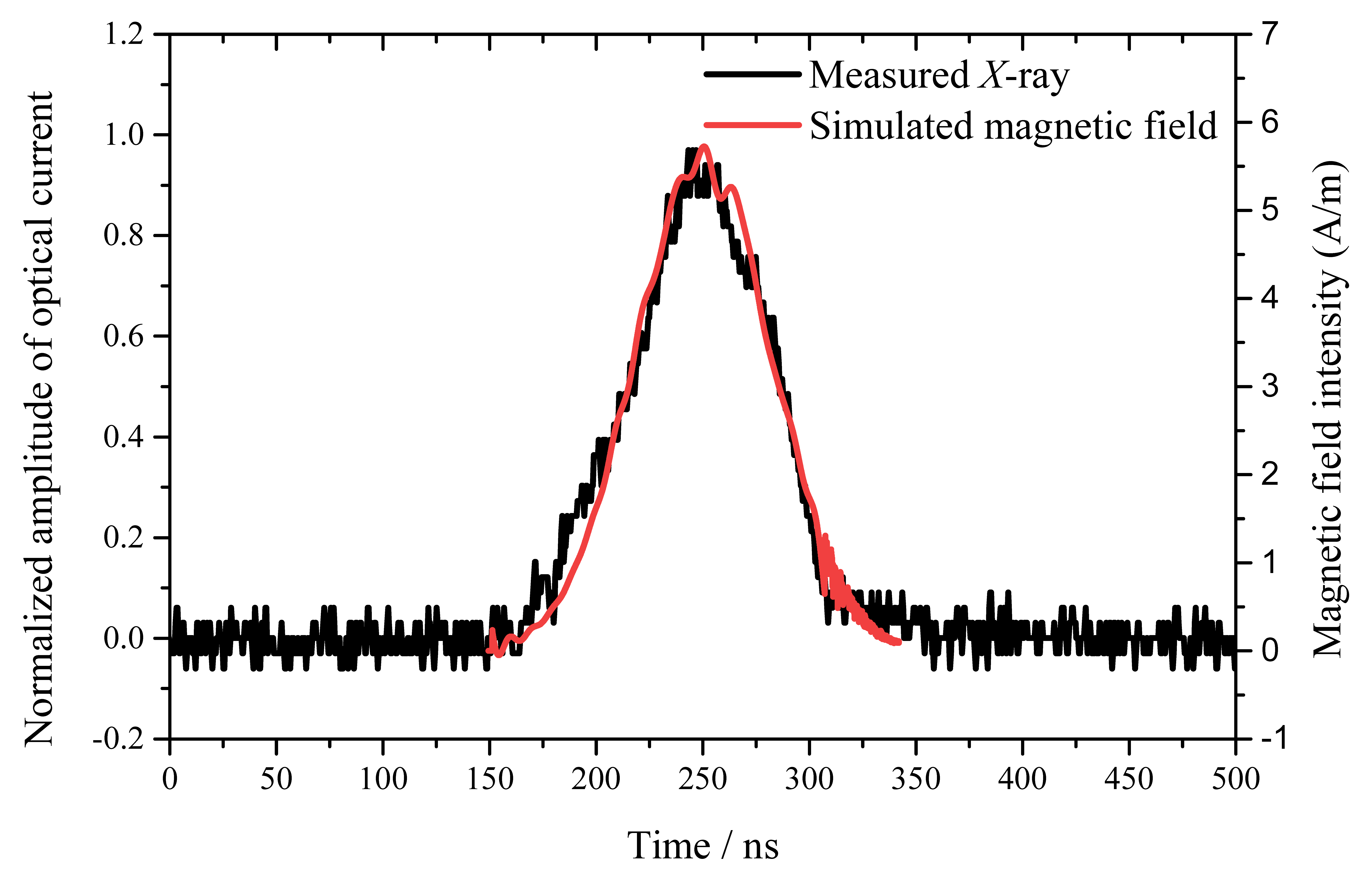
Referring to the method in [12], the SGEMP in the cavity is numerically calculated by employing the particle-in-cell and finite difference time domain methods with the “Flash II” hard X-ray accelerator wave of the Northwest Institute of Nuclear Technology as the irradiation source. The red curve in Figure 2 is the magnetic field waveform obtained by the simulation calculation, which can provide the basis for the detector index design. The black curve in Figure 2 is the measured X-ray waveform. The X-ray waveform characteristics used in the simulation calculation are consistent with the measured X-ray waveform in Figure 2 (the black curve). Because the calculation time of this simulation model is long, in order to reduce the calculation time, the calculation is terminated when the main waveform characteristics are calculated. In order to compare the characteristics of the X-ray and the magnetic field waveforms, we shifted the simulation waveform (the red waveform) in time and aligned their peaks.
As can be observed from Figure 2, the SGEMP magnetic field waveform is similar to the waveform characteristics of an X-ray source, and there are many sensitive parameters for the SGEMP response calculation, but the relevant research literature supports the main waveform characteristics of the SGEMP magnetic field signal [13,14]. According to the classical approximate estimation formula fH ≈ 0.35/tr for the pulse rise time tr and the corresponding signal frequency domain −3 dB bandwidth upper limit fH, it can be seen that the upper limit of the frequency of the SGEMP magnetic field signal to be measured is about 7 MHz. Furthermore, the SGEMP magnetic field strength calculated from the typical X-ray waveform of Flash 2 (average energy is about 120 keV) is less than 10 A/m (1.25 μT), which provides a clear basis for the design of a magnetoresistance detector.

3. Design and Calibration of Magnetoresistance Detectors

The internal structure of the proposed TMR sensor is shown in Figure 3. A push-pull Wheatstone bridge structure is formed by employing four highly sensitive TMR sensitive resistors. The resistance value of each tunneling resistor is equal. R1, R3, and R2, R4 have opposite magnetic sensitivity directions. The resistance variation ΔR in the external magnetic field is equal in magnitude and opposite in direction.
Common-mode interference to the sensor from the external environment can be eliminated by differencing the two output signals. The differential output signal Vout is:
V out = V o + V o = Vcc R + Δ R 2 R R Δ R 2 R = Vcc Δ R R

3.1. Design of Detectors

Based on the selected TMR sensing chip as the core, the designed detector hardware composition is shown in Figure 4. The differential mode is used for the differential output of the two output signals of the TMR chip. The amplifier mode is used for secondary amplification of the signal. The filter mode is used for low-pass filtering of the signal to eliminate high-frequency interference. The power mode is used to adjust the external input power between ±2.5 and ±5 V for the system power supply.
The internal sensitive resistance of the TMR sensor is thousands of ohms, which requires the input impedance of the differential module to reach the MΩ level. Here, the instrument operational amplifier INA849 is selected as the core device. Three operational amplifiers are integrated inside the operational amplifier, and the two operational amplifiers at the input port form a voltage follower to provide the high input impedance, reducing the circuit’s attenuation of the weak input signals. The latter stage of the operational amplifier is a fully differential amplifier to realize the subtraction operation of two channels of signals. It has a common mode rejection ratio of 90 dB and a frequency response bandwidth of 28 MHz at one time of gain, which can better meet the operating requirements.
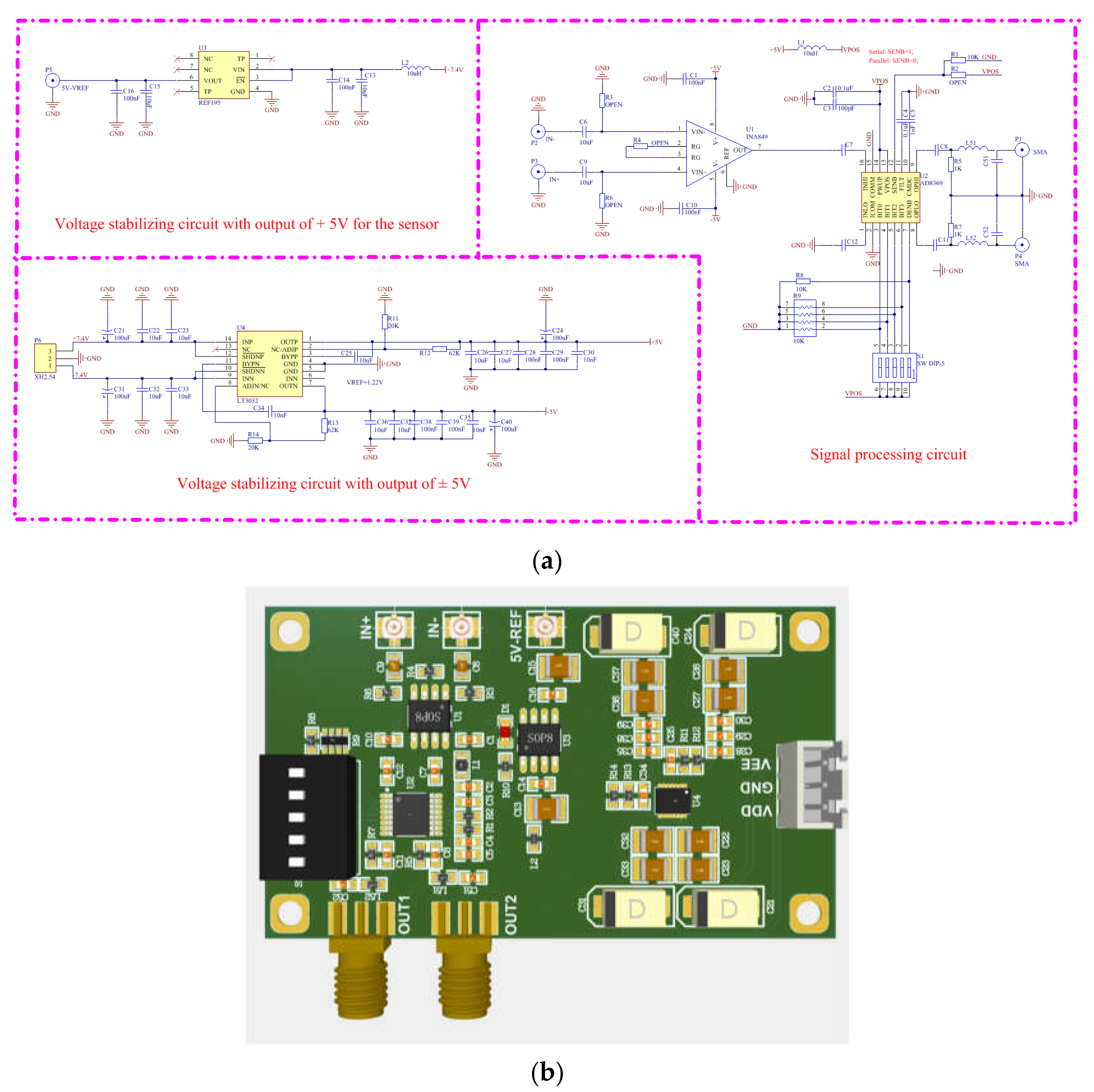
As the TMR sensor has a wide dynamic range in addition to a high magnetic field resolution, in order to take into account the measurement requirements for magnetic field signals of different intensities, the numerical control variable gain amplifier AD8369 is selected as the amplification module’s core. The device has an adjustable gain range of −5~40 dB (an adjustment step of 3 dB) under 1 k load output and a bandwidth of −3 dB at 600 MHz. Here, a digital switch is used to adjust and control the amplifier gain. The circuit schematic is shown in Figure 5a, which is composed of three parts. The first part is the voltage stabilizing circuit with an output of +5 V for the sensor. The second part is the voltage stabilizing circuit with an output of ±5 V for the sensor. The power supply regulator circuit in this work is designed based on the REF195 voltage reference chip. The third part is the signal processing circuit. Figure 5b shows the top view of the photograph of the designed and processed printed circuit board.
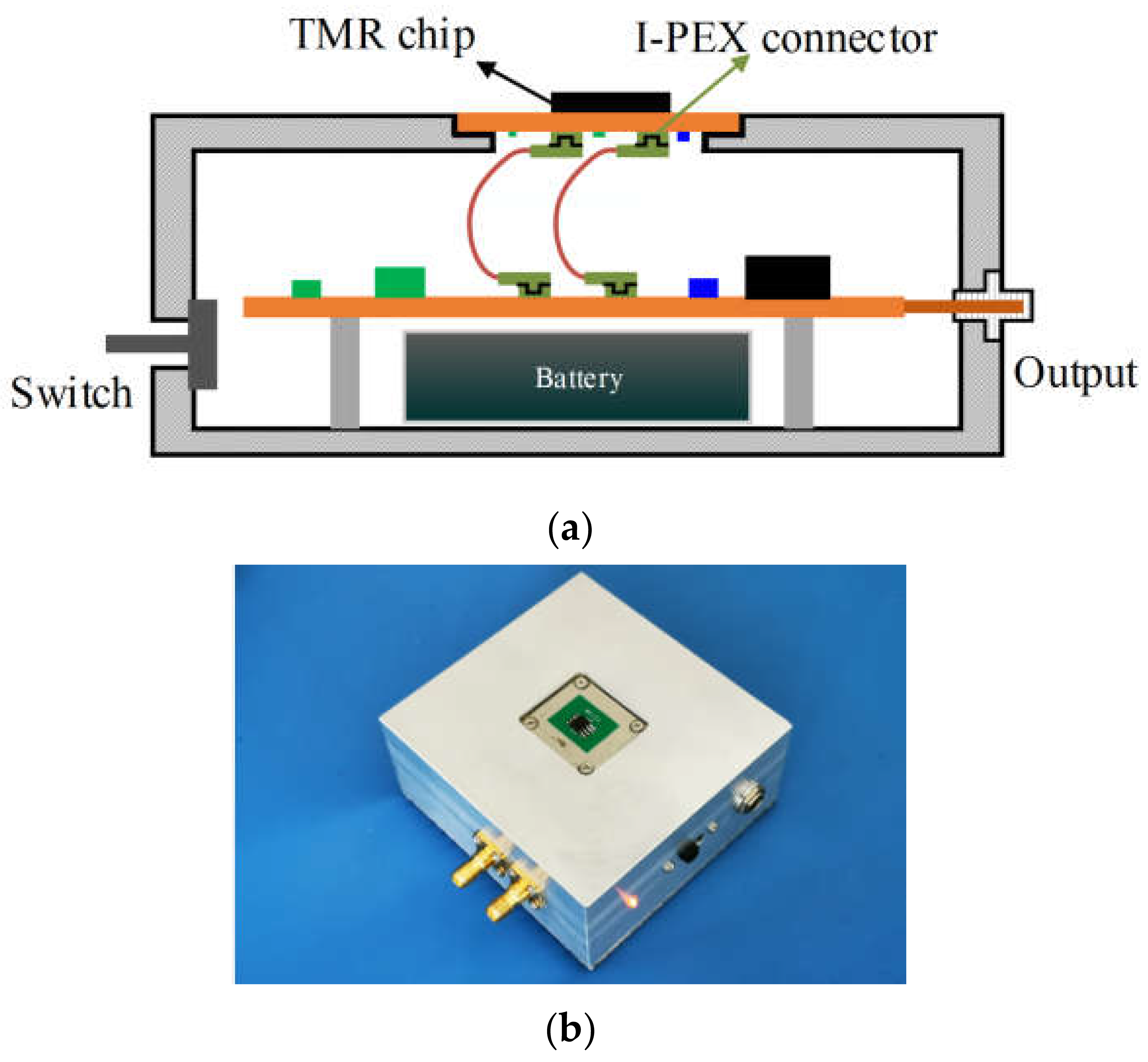
In order to adapt to the complex and harsh measurement environment, the detector also needs to have a good structural design to reduce the external exposure to the power lines and signal lines of the TMR sensor chip. The detector also needs to have good electromagnetic shielding performance to prevent the SGEMP electric field signal from interfering with the detector. The optimized detector structure is shown in Figure 6a. It contains a TMR chip, battery, switch, output port, and IPEX connector. Figure 6b shows the processed physical photograph.
The top layer and bottom layer of the circuit board fixing the TMR sensor chip are both covered with copper, and the copper covering at the overlapping part with the shell is exposed to ensure the good electrical connection and integrity of the shielding between the two layers. The TMR chip pins are routed to the bottom of the circuit board through a hole and are connected to the subsequent signal processing board by using the I-PEX connector with a 360-degree full shielding structure. Only the TMR sensing chip of the optimized detector is placed outside the shell to induce the magnetic field signal, which provides maximum protection to the internal circuit.

3.2. Calibration of Detectors

The sensitivity coefficient, frequency response bandwidth, and other indicators of the developed detector need to be calibrated before it is used. In this case, the TEM chamber is used as a standard field generator to generate pulsed electromagnetic waves for calibration [15]. The calibration method is shown in Figure 7.
A TEM chamber is a deformed transmission line structure in which an approximately uniformly distributed electromagnetic environment can be simulated. The upper limit of the operating frequency of the TEM chambers used is 500 MHz, and the distance d between the center conductor and the outer conductor is 15 cm. When the voltage difference between the inner and outer conductors is ΔU, the strength of the electric field E and magnetic field H formed in the interior are:
E = Δ U d , H = E η
where η is 377 Ω of wave impedance in free space.
Place the detector at the center point of the small chamber and set the internal amplifier circuit to the maximum gain mode. The output square wave pulse width of the pulse source is 200 ns, and the connected attenuator is 60 dB. The calibration scenario is shown in Figure 8.
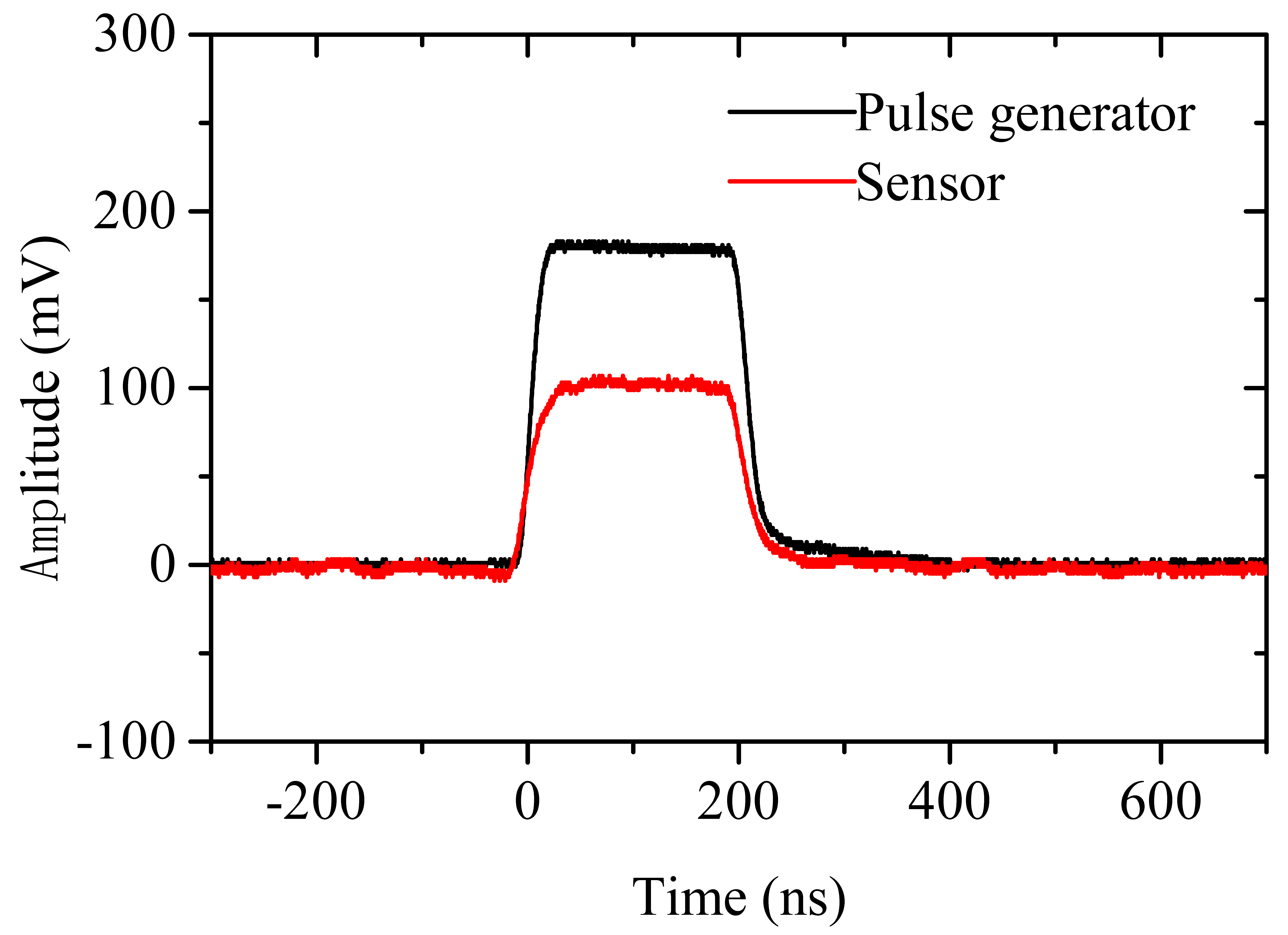
The calibration waveform at 180 V output of the pulse source is the black waveform, as shown in Figure 9, and the red waveform measured by the detector is consistent with the pulse source. Because the pulsed electric field energy in the TEM chamber is a strong interference signal compared with the magnetic field detector, the calibration waveform further proves that the detector has good anti-interference performance.
The output amplitude of the square wave pulse source is continuously increased, and the group calibration data is linearly fitted to obtain the detector sensitivity coefficient S = 4.0 nT/mV. The leading time of the measured waveform of the detector is 28 ns. According to the approximate estimation formula, the upper limit of the frequency of the detector is about 12 MHz. The calibration results show that the sensitivity coefficient and frequency response index of the detector can meet the requirements of the experimental measurement.

4. Measurement and Analysis of SGEMP

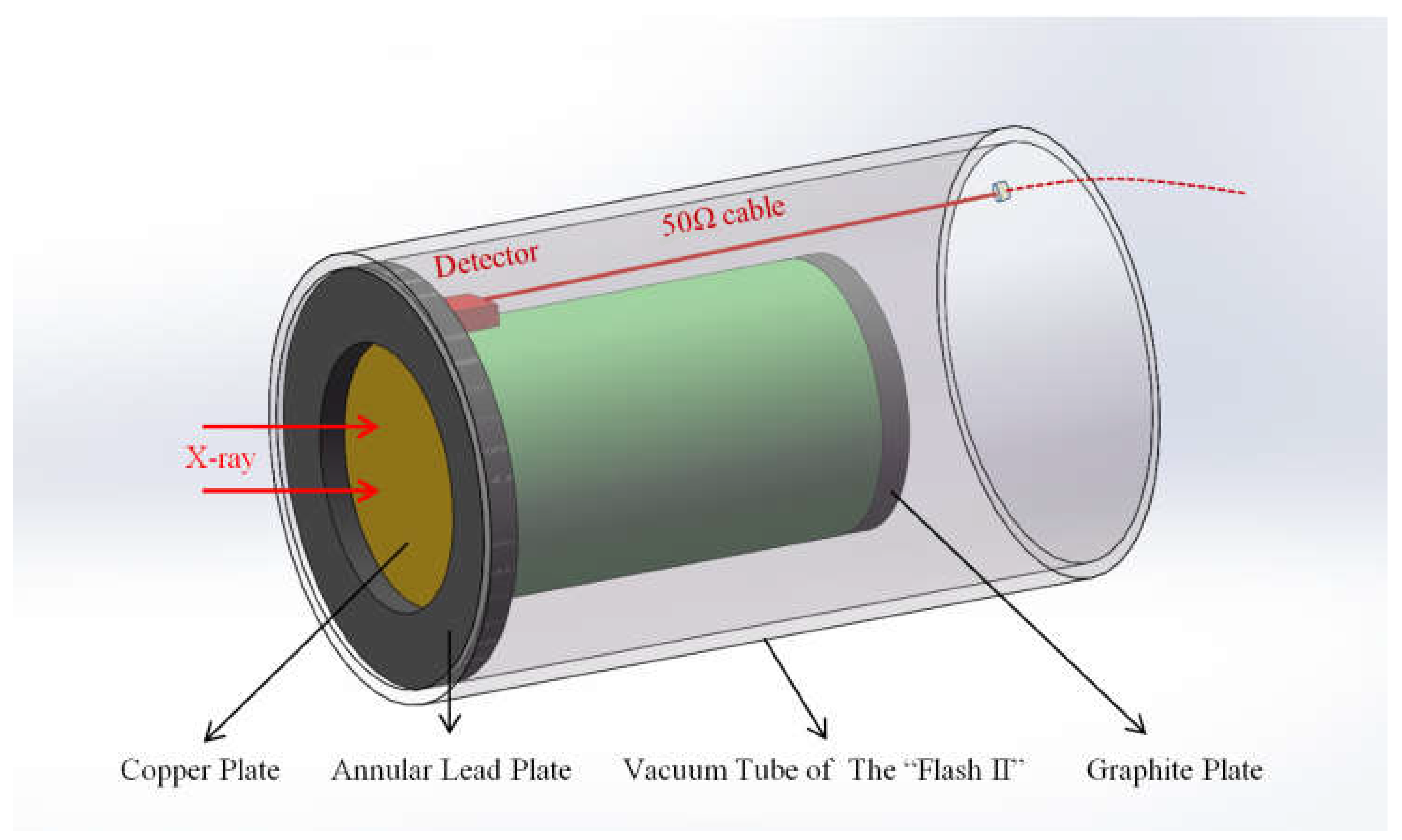
In order to verify the feasibility of the technical scheme, experimental verification is carried out under the “Flash II” hard X-ray accelerator based on the developed detector. The experimental design is shown in Figure 10. The designed cavity is a cylindrical aluminum cavity with a diameter of 20 cm and a wall thickness of 2 mm. Its front panel is a copper plate with a thickness of 1 mm (easy to excite electrons). The back panel is 3 mm thick and made of graphite material (used to absorb photoelectrons). The front end of the cavity is provided with a 5 mm square hole, and therefore the TMR chip of the detector can be inserted into the inner wall of the cavity to sense the SGEMP magnetic field signal. To reduce error, the TMR chip is placed as far as possible in the center of the TEM cell.
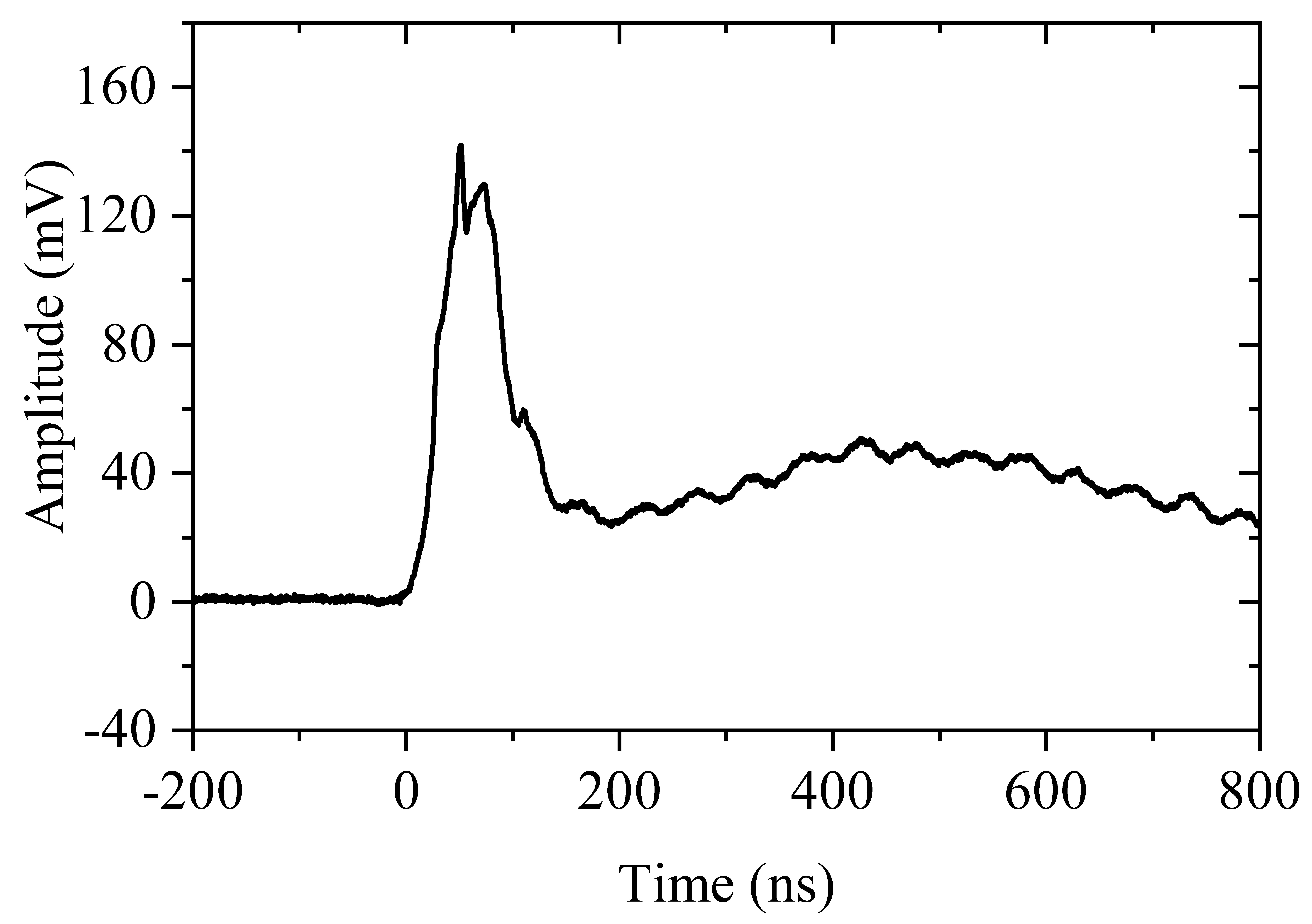
In order to avoid direct exposure of X-rays to the detector, an annular lead plate with a thickness of 200 mm is placed at the front of the cavity. The output signal of the detector is led to the outside of the vacuum tube through a coaxial cable. In this work, the RF1.13 coaxial cable is selected to match with the IPEX connector mainly because of its advantages of miniaturization and 360° shielding. In addition, the signal is transmitted to the measurement shield room by the optical fiber transmission system for signal acquisition and recording. The typical experimental measurement waveform is shown in Figure 11. The signal returning to zero cannot be observed due to the limitation of the oscilloscope data record length. We think there may be some interference. However, the observation of the peak signal is not affected. As the distance from the total current source increases, the magnetic field strength gradually decreases. In this work, the distance from the wall where we calculated the magnetic field strength is 1 cm. There are some ripples in Figure 11. We think there may be two reasons. The first is that the ground of the designed measurement system is connected with the ground of the “Flash II” X-ray source. As the working voltage of “Flash II” is very high (hundreds of kilovolts), the ripple in Figure 11 may be affected by the ground signal. The second is that the trigger signal of the oscilloscope is given by a “Flash II” source. The trigger signal amplitude is very large, and it is connected to the oscilloscope after attenuation.
Because the measurement environment is too complex, the measurement results are still inevitably superimposed with some interference. However, since the output of the detector is the time-domain waveform of the signal to be measured, the measurement results are easily distinguished from the main peak waveform of the useful signal. Meanwhile, the main peak waveform is basically composed of X-ray light waveform characteristics. The converted peak magnetic field strength is 4.5 A/m, which is basically consistent with the theoretical results. After the main peak, the signal returns to zero slowly for a period of time. The slow zeroing situation may be due to the coaxial cable inside the “Flash II” vacuum drift tube being affected by the deposition of photoelectrons, which resulted in a relatively slow capacitive discharge phenomenon. To try to solve the problem, the next step is also proposed: integrate the electro-optical conversion circuit inside the detector and transmit the measurement signal using a full-link optical fiber.

5. Conclusions

This paper proposes a technical solution for SGEMP magnetic field measurement based on the magnetoresistance effect. With a TMR sensor chip as the core, a pulse magnetic field detector with strong anti-interference ability is developed with common mode suppression, filtering, and shielding structure design. Moreover, the ideal measurement waveform is obtained under the “Flash II” hard X-ray pulse source, which proved the feasibility of the technical solution. These results have laid the foundation for further SGEMP numerical calculations and effect studies. The electron yield after interaction of different energy spectrum X-rays with metal materials varies. The range of electrons varies with their energy spectrum. The atmospheric pressure in the cavity will also affect the movement of internal electrons. These factors lead to a relatively complex SGEMP environment in the cavity. The next step is to carry out the SGEMP measurement under conditions of different energy spectrums of X-ray, different metal materials, and different cavity pressures based on the developed detector. Furthermore, the detector has the advantages of a small size, excellent high-frequency characteristics (12 MHz), high measurement sensitivity (4.0 nT/mV), and spatial “point” magnetic field measurement. Except for the SGEMP magnetic field signal measurement, the designed detector has a broader application prospect in the fields of lightning pulse magnetic field measurement, magnetic field shielding effectiveness measurement of cavities, and metal surface current measurement.

Author Contributions

Design and fabrication of the proposed structure and system, Y.L., W.W., J.L. and M.Z.; contributed to the discussion and manuscript—review, S.R. and T.H.; manuscript—revision, F.W. All authors have read and agreed to the published version of the manuscript.

Funding

Project supported by National Key Laboratory of Intense Pulsed Radiation Simulation and Effect (SKLIPR1702).

Institutional Review Board Statement

Not applicable.

Informed Consent Statement

Not applicable.

Data Availability Statement

Data is unavailable due to privacy.

Acknowledgments

Thanks for the help of Jianbo Wang from the School of Physical Science and Technology, Lanzhou University and Jun Hu from Department of Electrical Engineering and Applied Electronics Technology, Tsinghua University with magnetoresistive sensing chips.

Conflicts of Interest

The authors declare no conflict of interest.

References

  1. Rich, W.F.; Stringer, T.A. System-generated electromagnetic pulse and spacecraft charging effects: A review of the technology as applied to system hardening problems. IEEE Trans. Nucl. Sci. 1980, 27, 1523–1528. [Google Scholar] [CrossRef]
  2. Longmire, C.L. On the electromagnetic pulse produced by nuclear explosions. IEEE Trans. Antennas Propag. 1978, 26, 3–13. [Google Scholar] [CrossRef]
  3. Higgins, D.F.; Longmire, C.L.; O’Dell, A.A. A Method for Estimating the X-ray Produced Electromagnetic Pulse Observed in the Source Region of a High-Altitude Nuclear Burst; Mission Res. Corp: Santa Barbara, CA, USA, 1973. [Google Scholar]
  4. Woods, A.J.; Delmer, T.N. The arbitrary body of revolution code (ABORC) for SGEMP/IEMP. In Topical Report, September 1975–June 1976. United States; IRT Corp.: San Diego, CA, USA, 1976. [Google Scholar]
  5. Cui, M.; Zhiqian, X.; Yunsheng, J.; Wanguo, Z.; Zhao, D. Numerical simulation of the SGEMP inside a target chamber of a laser inertial confinement facility. IEEE Trans. Nucl. Sci. 2017, 64, 2618–2625. [Google Scholar] [CrossRef]
  6. Chen, J.; Wang, J.; Chen, Z.; Ren, Z.; Qiao, H. Study of SGEMP Field-Coupling inside and outside reentrant cavity. IEEE Trans. Electromagn. Compat. 2022, 64, 1182–1189. [Google Scholar] [CrossRef]
  7. Cheng, Y.; Zhou, H.; Li, B.; Chen, M.; Wu, W.; Qiao, D. Simulation of system-generated electromagnetic pulse caused byemitted photoelectron in cavity. High Power Laser Part. Beams 2004, 16, 1029–1032. [Google Scholar]
  8. Zhou, Y.; Cheng, Y.; Zhu, Z.; Ma, L.; Chen, P.; Wang, W.; Wang, X. Simulation study of air Effects on SGEMP based on Swarm Mode. IEEE Trans. Nulear Sci. 2022, 69, 26–34. [Google Scholar] [CrossRef]
  9. Zhang, H.; Zhou, Q.; Zhou, H. Effect of secondary electron emission on SGEMP. Acta Phys. Sin. 2021, 70, 195–203. [Google Scholar]
  10. Zhou, K.; Wang, Y.; Deng, J. Development and test of measurement system for cable system generated electromagnetic pulse effects. High Power Laser Part. Beams 2014, 26, 175–179. [Google Scholar]
  11. Lenz, J.; Edelstein, A.S. Magnetic sensors and their applications. IEEE Sens. J. 2006, 6, 631–649. [Google Scholar] [CrossRef]
  12. Li, J.; Wu, W.; Guo, J.; Liu, Y.; Zhao, M.; Ma, L.; Cheng, Y. Verification of numerical simulation model for SGEMP generated in Flash-Ⅱ accelerator environment. Mod. Appl. Phys. 2016, 7, 26–30. [Google Scholar]
  13. Chen, J.; Wang, J.; Tao, Y.; Chen, Z.; Wang, Y.; Niu, S. Simulation of SGEMP using particle–in-cell method based on conformal technique. IEEE Trans. Nucl. Sci 2019, 66, 820–826. [Google Scholar] [CrossRef]
  14. Wu, W.; Zhao, M.; Li, J.; Zhou, H. Study on the parameters of cavity system-generate electromagnetic pulse (SGEMP) calculation model base on Maxwell-Valsov equation. In Proceedings of the IEEE 3rd International Conference on Automation, Electronics and Electrical Engineering, Shenyang, China, 20–22 November 2020; pp. 484–487. [Google Scholar]
  15. Karst, J.P.; Groh, C. Calculable field generation using TEM cells applied to the calibration of a novel E-Field probe. IEEE Trans. Electromagn. Compat. 2002, 44, 59–71. [Google Scholar] [CrossRef]
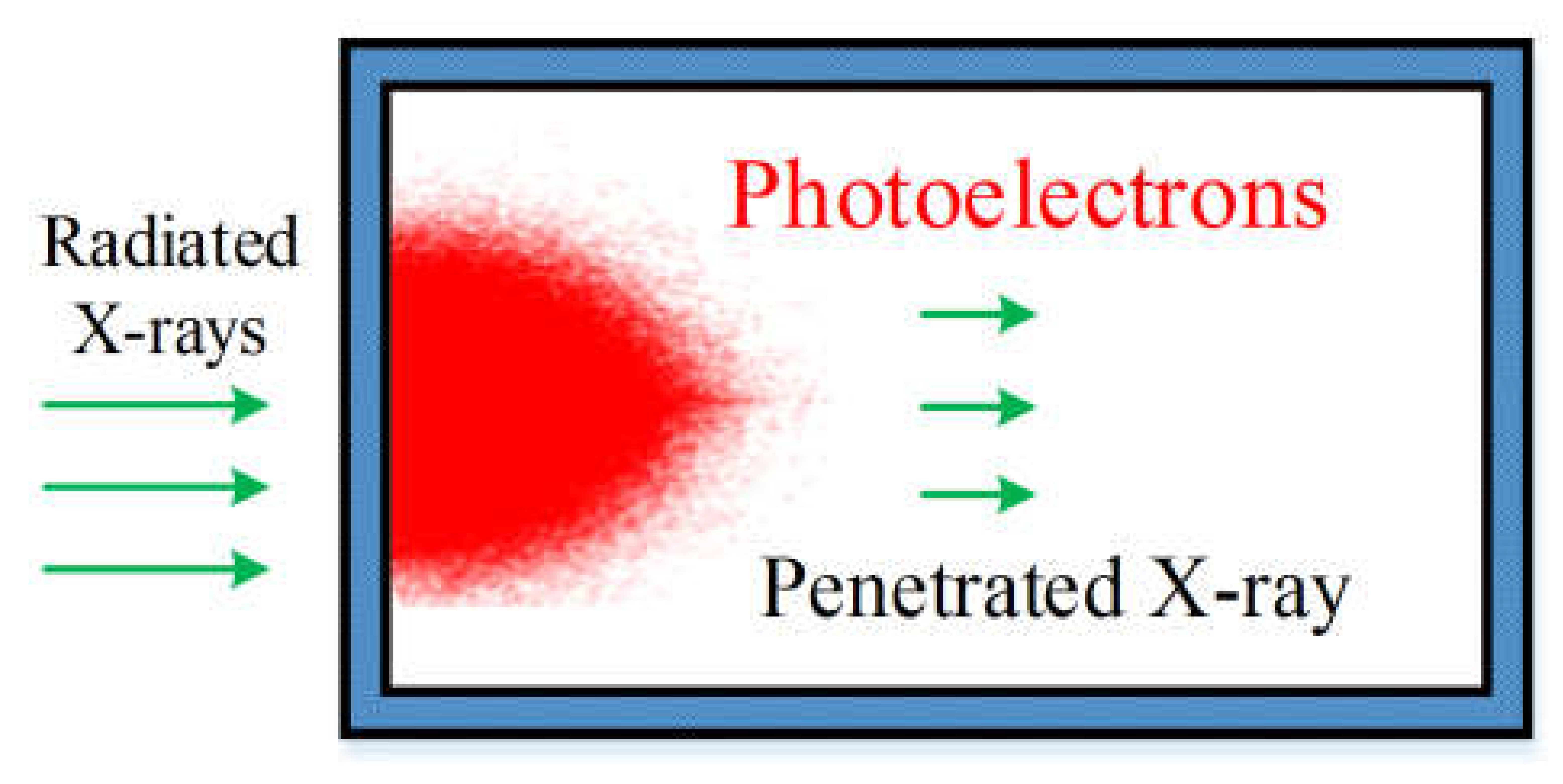
Figure 1. Simplified SGEMP model under X-ray irradiation.
Electronics 12 00492 g001
Figure 2. X−ray waveform and SGEMP simulation waveform.
Electronics 12 00492 g002
Figure 3. The equivalent Wheatstone bridge model of the TMR sensor.
Electronics 12 00492 g003
Figure 4. Hardware circuit block diagram.
Electronics 12 00492 g004
Figure 5. (a) Circuit schematic, (b) top view of the PCBA of the proposed hardware circuit.
Electronics 12 00492 g005
Figure 6. (a) Configuration and (b) photograph of the designed detector.
Electronics 12 00492 g006
Figure 7. Schematic diagram of detector calibration.
Electronics 12 00492 g007
Figure 8. Scenario of detector calibration.
Electronics 12 00492 g008
Figure 9. Typical calibration waveform.
Electronics 12 00492 g009
Figure 10. Measurement scheme for the magnetic field signal of the SGEMP.
Electronics 12 00492 g010
Figure 11. Typical SGEMP measurement waveform.
Electronics 12 00492 g011
Disclaimer/Publisher’s Note: The statements, opinions and data contained in all publications are solely those of the individual author(s) and contributor(s) and not of MDPI and/or the editor(s). MDPI and/or the editor(s) disclaim responsibility for any injury to people or property resulting from any ideas, methods, instructions or products referred to in the content.