Article

FPGA-Based Tactile Sensory Platform with Optical Fiber Data Link for Feedback Systems in Prosthetics

1
Department of Industrial and Information Engineering and Economics, University of L’Aquila, 67100 L’Aquila, Italy
2
COSMIC Lab, Department of Electrical, Electronic, Telecommunications Engineering and Naval Architecture, University of Genova, 16126 Genova, Italy
3
EPICS Lab, Department of Information Engineering Computer Science and Mathematics, University of L’Aquila, 67100 L’Aquila, Italy
4
Department of Electrical and Electronics Engineering, Lebanese International University (LIU), Beirut 1105, Lebanon
*
Author to whom correspondence should be addressed.
Electronics 2023, 12(3), 627; https://doi.org/10.3390/electronics12030627
Submission received: 31 December 2022 / Revised: 15 January 2023 / Accepted: 18 January 2023 / Published: 27 January 2023
(This article belongs to the Special Issue Feature Papers in Circuit and Signal Processing)

Abstract

:
In this paper, we propose and validate a tactile sensory feedback system for prosthetic applications based on an optical communication link. The optical link features a low power and wide transmission bandwidth, which makes the feedback system suitable for a large number and variety of tactile sensors. The low-power transmission is derived from the employed UWB-based optical modulation technique. A system prototype, consisting of digital transmitter and receiver boards and acquisition circuits to interface 32 piezoelectric sensors, was implemented and experimentally tested. The system functionality was demonstrated by processing and transmitting data from the piezoelectric sensor at a 100 Mbps data rate through the optical link, measuring a communication energy consumption of 50 pJ/bit. The reported experimental results validate the functionality of the proposed sensory feedback system and demonstrate its real-time operation capabilities.

1. Introduction

Recent technological innovations have proposed new opportunities to develop advanced prosthetic devices that can replace human counterparts. Most prosthetics do not provide sensory feedback, making the holding and manipulation of objects a difficult task for the user [1]. To address and overcome this difficulty, the design of new sensory feedback systems is an active area of research for both prosthetics [2] and robotics [3].
The tactile sensory feedback system consists of (i) an array of tactile sensors that are connected to (ii) an electronic interface circuit that acquires the sensor signals and converts them into a digital format and (iii) a digital processing unit that extracts meaningful information [4] delivered to the prosthetic user through (iv) an electrotactile stimulator [5].
There has been a significant amount of research aiming to improve the motor control of prosthetics including its tactile sensory feedback system. Efforts in this field have been focused on developing various types of tactile sensors (e.g., capacitive [6], resistive [7] and piezoelectric [8]), and on designing efficient interface electronics [9]. However, to our knowledge, no study has focused on the communication channel from sensors to the electrotactile stimulator. A large number of sensors are needed for obtaining human-like touch-sensing capabilities [10]. This imposes challenges on the system design in terms of power consumption, real-time operation and data transmission bandwidth.
The key contribution of this paper is the design of an optical communication link connecting the sensors to the tactile electrostimulation. The assembled system prototype is composed of both the digital transmitter and receiver boards and an analog acquisition circuit that interfaces piezoelectric sensors. The system can acquire, process and transmit the information of 32 sensors at a 100 Mbps transmission data rate with a power consumption of 50 pJ/bit. Compared to the standard communication protocols used for data exchange such as Bluetooth, CAN bus, SPI and UART [11,12], the presented architecture provides a higher transmission rate and lower power consumption, achieved through an optical pulsed data-coding technique inspired by UWB-IR systems [13,14].
This paper is an extension of the work previously published in [15] and includes a complete description of the system with additional details on each electronic and optoelectronic constitutive block. In addition, the transmission pulsed coding technique is fully explained, and a prototype that transmits data from real sensors to the electrotactile stimulator has been experimentally validated and reported.
This paper is organized as follows: Section 2 reviews the literature regarding recent advances in sensory feedback systems. The proposed system architecture including tactile sensor fabrication, data acquisition and transmission blocks is detailed in Section 3. Section 4 describes the experimental setup used to evaluate the overall system and presents and discusses the achieved experimental results. Conclusions are included in Section 5.

2. Review of the State-of-the-Art

To the best of our knowledge, there is no study that addresses the data transmission channel of a sensory feedback system either in prosthetic or robotic applications. This section reviews the recent developments in sensory feedback systems, highlighting the communication protocols used to transmit tactile sensor data.
Aiming for the reconstruction of hand posture and tactile information, authors of [16] proposed a multi-modal sensing glove composed of piezoresistive fabric for measuring normal forces with more than 50 taxels spread over the palm surface. During manipulation, force was recorded through a data acquisition board: each single sensor was connected to a voltage divider and an analog-to-digital converter (ADC). A PIC18-microcontroller was used on the acquisition board to collect sensor data and transmit them via USB to the host PC. The sensory system of a robotic arm in [17] included large patches based on commercial force sensors to cover large areas of the arm. Each patch had 16×9 force sensors sampled at 78 frames per second through an acquisition board. A PIC18F4680 was in charge of (i) scanning the array of sensors, (ii) sorting data and (iii) transmitting them via CAN bus communication to a central processing unit. In [18], the tactile sensory system for robotic hands provided distributed pressure measurements and information on the contact location obtained during interaction with the environment. The design was based on integrating a large number of capacitive sensors structured in a mesh of 16 interconnected sensing units. Each sensing unit carried 12 taxels with a charge-to-voltage converter and shared an I2C bus with a master unit. The master unit received the sensor data and transmitted them to the PC through a CAN bus.
Delivering tactile information from sensors to the user remains a challenge. Researchers are investigating methods that provide useful tactile information in both prosthetics [1,19] and robotic hands, such as applied forces, object texture and slippage. The sensing feedback system in [1] enabled the prosthetic user to feel various objects touched by means of electrotactile stimulations. The system was composed of 16 resistive film force sensors connected to a control board. The microprocessor on the control board collected the sensor data at 20 samples per second and sent them to a PC via USB. The data in the PC were processed and sent through a USB wireless transmitter to the user as electrotactile-stimulation feedback. A similar approach with different stimulation modalities was proposed in [19] to improve the recognition rate and reduce the mental workload when identifying different stimulation patterns. The system incorporated vibro-tactile and mechano-tactile modalities. The system consisted of five piezoelectric tactile sensors which were multiplexed to a low-energy communication module (CC2640R2F). The sensory data were combined into packets and then sent via Bluetooth to the customized-design multi-modal stimulator. Regarding robotic hands, authors in [4] introduced a sensing system based on robotic fingertips containing four force and two PVDF sensors. The system could detect normal contact and slip forces applied on the surface of robotic fingertips. The signals coming from different PVDF sensors were received by six ADC converters on a microcontroller-based board (C8051F311) and then transmitted to the PC via RS232 or SMBus. Thus, integrating multiple fingertips will make collecting large numbers of data a complex task and, consequently, will require transmission links with a wide bandwidth.
However, some approaches have addressed the embedded electronics (e.g., the sensor interface electronics) of the tactile sensing system in both prosthetics and robotics [20,21]. The employment of a larger number of taxels will result in the need for a wider bandwidth in order to transfer the increased amount of data. Moreover, approaches in [20,21] explored dedicated interface electronics for a wearable sensing system. In particular, in [20], a miniaturized interface electronics could acquire 32-PVDF sensor data simultaneously. The design was based on an off-the-shelf analog-to-digital converter (DDC232) and a low-power ARM-microcontroller. The sensory data were sampled and pre-processed before being transmitted through a Bluetooth channel to the stimulator connected at the user side. The system design reported in [21] was based on a single chip containing the digital microcontroller and 13 charge-sensitive analog front ends. The chip measured and locally processed the information generated by the taxels, taking into consideration the limited transmission bandwidth offered by the Bluetooth and USB interfaces. The pre-processed data were then sent to the PC through a USB to a UART converter chip. Detailed practical examples of systems for tactile applications were reported in [22,23]. In particular, the system in [22] was composed of a flexible array of 16 sensors integrated on the index finger, an analog-to-digital converter (DDC232), a programmable communication module (BL600) and a multichannel stimulator connected to a flexible array of 24 electrodes. This system was successfully tested in six able-bodied patients who were asked to recognize static patterns with two different spatial resolutions and dynamic movement patterns presented on the electronic skin. Starting from the systems such as the one described in [22], the key contribution of this paper is to replace the radio communication links employed, for example, in [24,25], with a specifically designed optical communication link connecting the sensors (i.e., the taxels) to the tactile electrostimulation. Compared to other wireless-based solutions, the proposed optical link improves the overall system bandwidth, achieves a higher level of electromagnetic compatibility and signal integrity, and optimizes power consumption efficiency.

3. System Architecture: Design and Implementation

The proposed system architecture is shown in Figure 1. The system mainly consists of a transmitter and a receiver connected through an optical communication link. The transmitter board is connected to a data acquisition system that interfaces the tactile sensors while the receiver board is connected to an electrotactile stimulator. The interfacing of multiple tactile sensors is challenging since continuous sampling is required. This challenge is addressed by adopting a commercial data acquisition circuit that integrates, converts and stores charge measurements of all input sensors simultaneously, as detailed in the following subsections. The transmitter is designed to perform data coding by a UWB-inspired pulsed modulation technique [13,14] that optimizes the overall system power consumption by reducing the temporal duration of the employed light signals (i.e., laser pulses). Finally, the receiver communicates directly with the prosthetic user through the electrotactile stimulation by means of a direct connection through a USB port translating the tactile sensor data into stimulator commands. The receiver has a shared global data buffer to store the decoded/recovered data and is capable of sending the processed data to a PC (through a UART interface) and/or an oscilloscope for visualization.
In the following subsections, we describe in more detail each part comprising the complete system.

3.1. The Tactile Sensors

For the present application, a PVDF-based sensory array was used to demonstrate the proposed system architecture. Tactile sensors based on piezoelectric materials, e.g., polymers such as PVDF, operate in the frequency range of 0 up to 1 KHz [26] and produce electrical charges proportional to the mechanical stress. When a touch/force is applied to the surface of a sensor, a mechanical deformation of the piezoelectric material occurs. This produces an electrical charge at the sensor output. When force is released, an output charge of opposite polarity occurs. This results in an alternating bipolar signal that requires dedicated circuits to be acquired.
The fabrication process of the sensor array encapsulates the P(VDF-TrFE) piezoelectric polymer between two electrodes [27]. First, a circular bottom electrode is screen-printed on a transparent and flexible substrate. Then, a P(VDF-TrFE) ferroelectric polymer is attached to the bottom electrode, followed by screen-printing of the top electrode. A final protection layer is then deposited on top of the sensor. In order to validate the fabrication process, an electromechanical test was performed on a set of sensing patches [28]. An electromechanical setup was used to perform continuous indentation to the sensor taxel over the whole frequency range of interest for tactile applications (less than 1 Hz up to 1 kHz). Then, the d33 piezoelectric coefficient was estimated since its measurement is a practical tool to study the behavior of each sensor. The average value of the d33 piezoelectric coefficient of the fabricated sensors was aligned to the expected ones found in the literature. Therefore, our fabricated sensing system could be used as real sensor data.

3.2. The Data Acquisition System

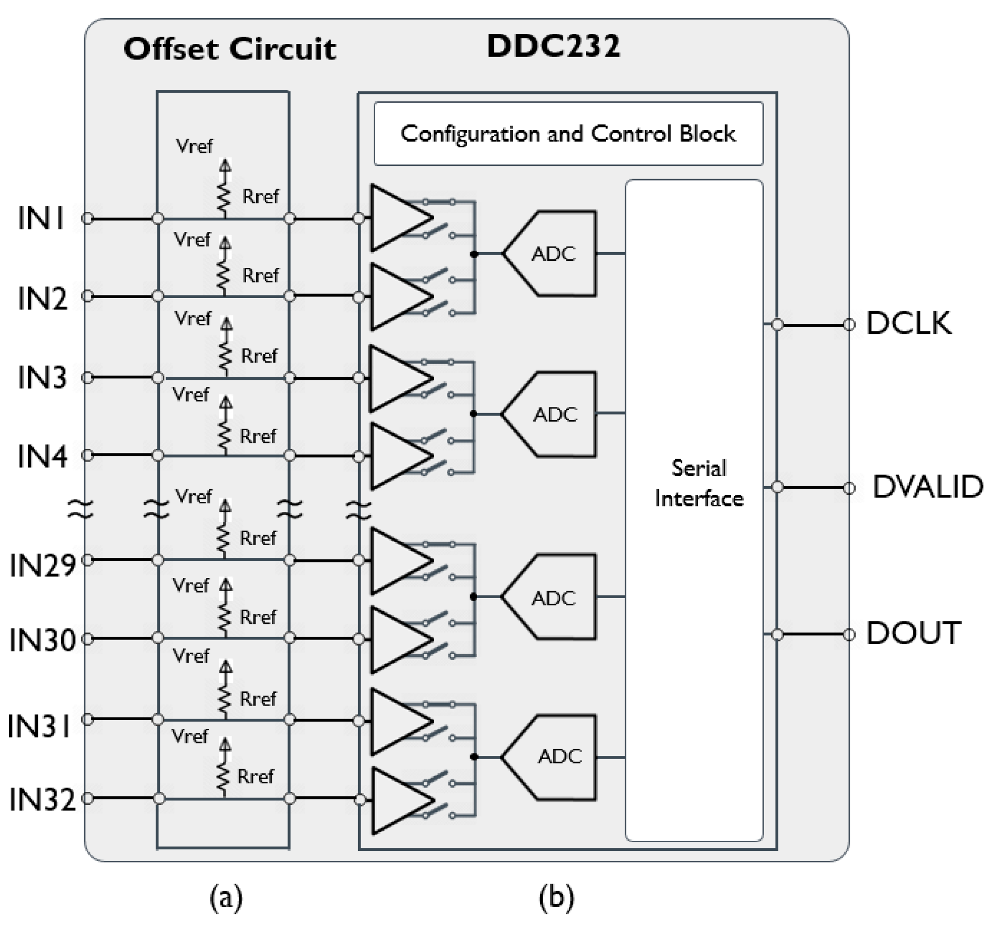
The block diagram of the data acquisition system is shown in Figure 2. It consists of (i) an offset circuit and (ii) a commercial current-input analog-to-digital converter (DDC232 [29]) that interfaces 32 input sensor channels. The offset circuit enables the acquisition of bipolar charge signals and is composed of a voltage source (Vref) connected in series to a resistor Rref, as shown in Figure 2a. This circuit produces an output signal that swings below and above Vref/2, thus passing both signal polarities to the DDC232 converter.
The architecture of the DDC232 is shown in Figure 2b. The DDC232 combines an integrator and a delta-sigma analog-to-digital converter. The integrator converts the generated charge into a proportional voltage and the delta-sigma ADC samples and converts the voltage at the output of the integrator to digital signals.
Each input channel is connected to a dual-switched integrator front-end, resulting in 64 integrators for all 32 input channels. This architecture allows for a continuous current-to-voltage integration where the output of the integrators from one side of the inputs is digitized while the other integrators are in the integration mode.
The output of the 64 integrators is switched to 16 delta-sigma converters via multiplexers. The result of the ADC conversion is stored in a shift register that holds the data of 32 channels.
The DDC232 comprises two digital blocks to control and adjust the configuration parameters to match the sensor signal characteristics: (a) the configuration block configures the parameters such as the feedback capacitance, data output format (16-Bit or 20-Bit) and the device version setting to be controlled by the software; (b) the digital interface block outputs the digital results via a synchronous serial interface consisting of clock and data pins. The data clock (DCLK), data valid (DVALID) and data output (DOUT) pins are used to retrieve the sensor data. Data retrieval begins after the signal DVALID goes low, indicating that data are ready and stored in the shift register. During reading, data are shifted out serially on the DOUT pin on the rising edge of DCLK.
The data acquisition system is configured and controlled by the Transmission Board, inside the optical communication link, which is implemented on an FPGA device. Its specifications are described in the following sections.

3.3. The Optical Communication Link

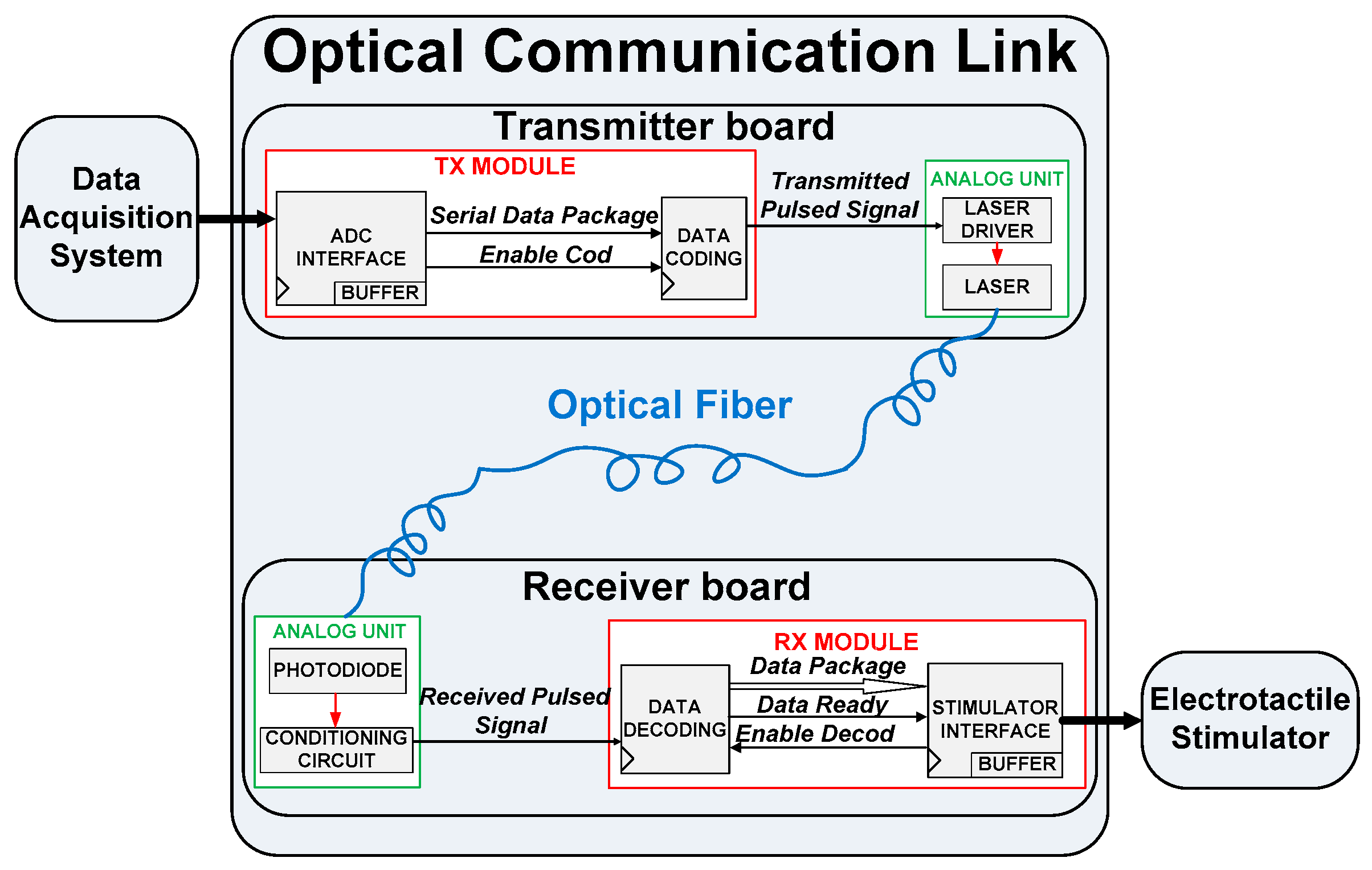
Figure 3 shows the block scheme diagram of the optical communication link composed of two sub-systems: the transmitter board and the receiver board, which are linked together through the optical fiber-based communication channel.
Referring to Figure 3, the transmitter board is composed of two blocks. The first block, TX module, is based on a fully digital architecture. The ADC interface controls the data acquisition system in order to generate a data package starting from the acquired digitally converted data. Moreover, the ADC interface performs a pre-processing elaboration of the incoming raw data by acquiring information coming from the only tactile sensors on which an event occurs. In the absence of events, no data package is sent to the RX module, establishing event-driven communication.
Once the acquisition has been accomplished, the serial data package bit stream is transmitted and the data coding block is enabled to perform the UWB pulsed coding of the data.
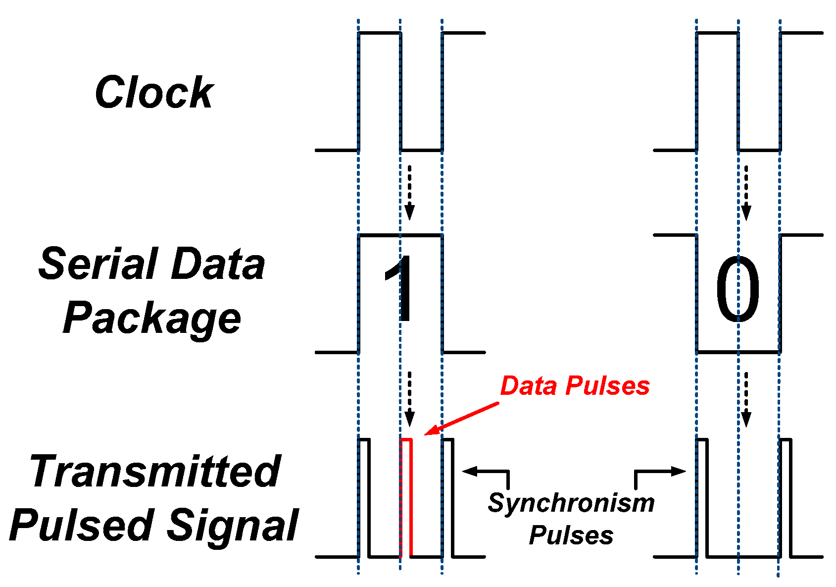
In this regard, referring to Figure 4, the data coding block always generates a “synchronism pulse” (used for the clock recovery operation in the RX module) in correspondence to the rising edge of a clock signal (synchronous with the data to be transmitted) and a “data pulse” on the falling edge of the same clock signals only if the bit to be coded from the serial data is equal to “1”. Thus, the output of this block is an aperiodic sequence of voltage pulses (i.e., the transmitted pulsed signal), which also contains the synchronization clock signal needed to properly receive the information/data contained in the signals generated by the sensors. The second block in the transmitter board, the analog unit, is composed of a vertical-cavity surface-emitting laser (VCSEL) and a laser driver that receives in input the sequence of the coded pulses and transforms them in a corresponding sequence of current pulses. The amplitude of these current pulses must exceed the value of the VCSEL threshold current to generate a corresponding sequence of laser pulses that is the optical replica of the coded signal. The generated laser pulses are then suitably coupled to the optical fiber that connects the transmitter board to the receiver board. Referring to Figure 3, the receiver board includes two main sub-blocks. The first sub-block is the analog unit composed of an analog conditioning circuit and a Si photodiode (PD), both with a frequency bandwidth equal to or larger than the VCSEL laser pulses that must be detected. Starting from the PD photogenerated pulsed current signals proportional to the intensity of the transmitted laser pulses, the conditioning circuit generates a sequence of voltage pulses (i.e., the electrical replica of the sequence of the laser pulses) and transmits the received pulsed signal to the RX module of the receiver board, which performs the decoding operation. Once the data package has been regenerated by the data decoding sub-block, this is sent to the stimulator interface, which is able to establish UART communication with the electrotactile stimulator.
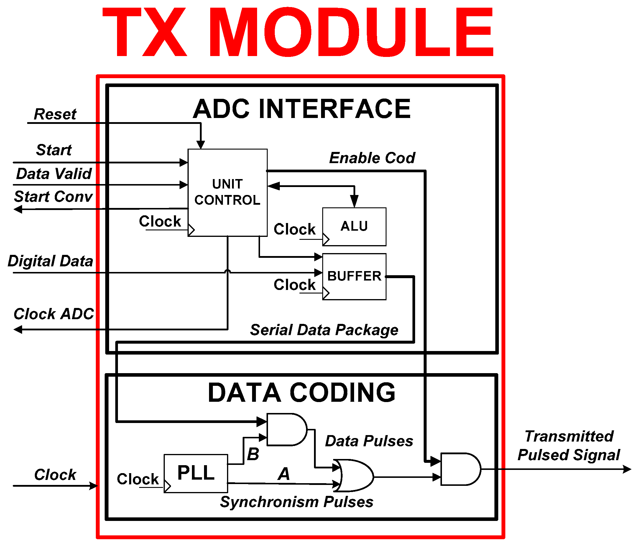
In more detail, the TX module architecture shown in Figure 5 was implemented in a Spartan6 FPGA (SP601 by Xilinx (San Jose, CA, USA)) that operated at a main clock frequency (i.e., clock) equal to 100 MHz. After a start signal goes high to the ADC interface block, the transmitter generates a proper Clock ADC signal connected to the DCLK pin of the DDC232 previously described.
Each time the transmitter toggles the signal Start Conv, the external ADC simultaneously scans and converts the analog signals generated by the array of sensors. The converted signals are shifted out to the acquisition module (i.e., the ADC interface block) through the digital data port at 2 kS/s each time the data valid signal, connected to the DVALID pin of the acquisition module, is set to a low logic state. Thus, when the data have been stored, the ADC INTERFACE generates a data package containing the data that must be transmitted (16 bits for each one of the 32 channels in which an event can occur), and a fixed sequence of bits is used as a header (i.e., the begin of the package). Then, the signal Enable_Cod goes high, enabling the digital coding block to perform the coding of the data stored in the buffer into a digital pulsed signal. In particular, the upper part of Figure 6 shows the serial data package to be sent, which consists of an orderly sequence of samples (each one corresponding to a specific sensor of the input array) and a header used to detect the beginning of the package. The lower part of Figure 6 reports the coding of the serial data package into the transmitted pulsed signal sent to the analog unit block of the transmission board. Only when a serial data package has been transmitted can a new acquisition be performed. All the control signals of the ADC interface block are managed by a control unit that uses the ALU unit for the timing and pre-processing operations. In addition, according to Figure 5, the data coding block was implemented by using a phase-locked loop (PLL) and few logic gates. The PLL, already realized as a basic block inside the FPGA, generates two pulsed signals, starting from the input clock signal. The first pulse at the PLL terminal A is generated in correspondence to the rising edges of the clock signal, and the second pulse at the PLL terminal B is generated synchronously with the falling edges of the clock signal. These two pulsed signals have the same frequency of 100 MHz with a relative phase difference of 180° and a selectable duty cycle to guarantee the desired pulse width (approximately 1 ns in this application). Combining the serial data package with signals A and B, the data coding block is able to send the transmitted pulsed signal at 100 Mbps.
The last part of the transmitter board is an analog unit composed of a driver circuit (i.e., the laser driver) that converts the voltage digital pulses into current pulses to drive the VCSEL (OPV314AT by TT Electronics (Woking, UK)), emitting at λ = 850 nm, with a response time lower than 100 ps.
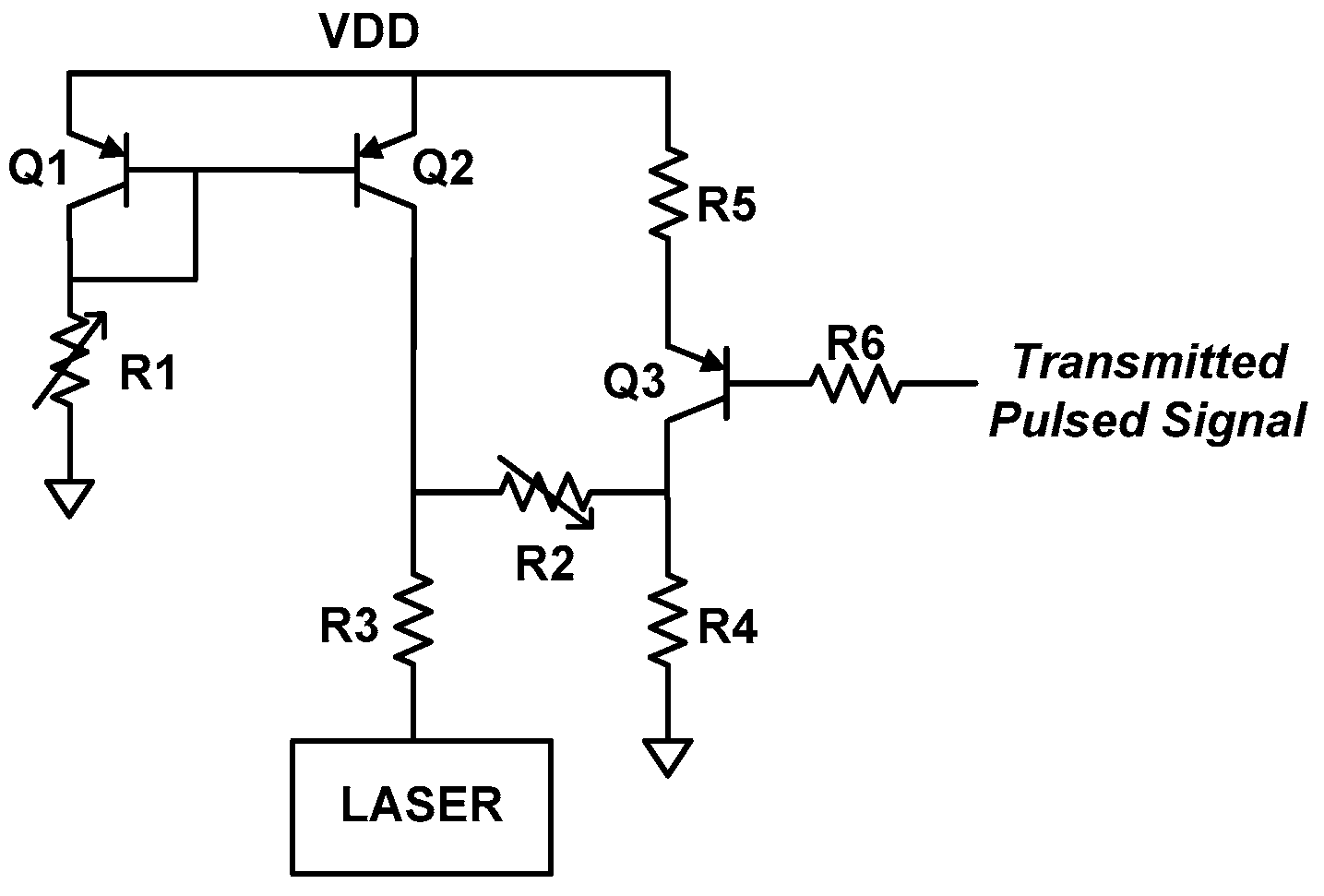
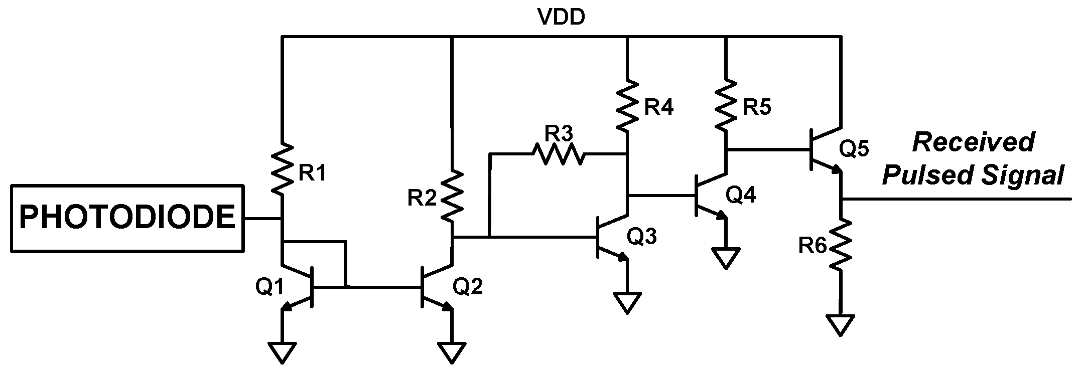
Figure 7 shows the schematic circuit of the laser driver based on a simple current-mirror topology. The variable resistors R1 and R2 (i.e., 470 W trimmers) allow for the regulation of the current pulse’s DC levels and AC amplitudes, respectively. The devices Q1, Q2 and Q3 are BFT92 5 GHz wideband PNP BJT transistors, while R3 = R5 = R6 = 33 Ω and R4 = 100 Ω. The VCSEL is coupled to one end of a 1 m length 50/125 µm multi-mode optical fiber, while the other end is coupled to a high-speed Si-based photodiode (PD, DET025AFC/M by Thorlabs) with rise/fall times of approximately 150 ps. The PD, located inside the receiver board, detects the transmitted laser pulses and generates their replica as photocurrent pulses. The PD is finally interfaced with a signal conditioning circuit that converts current pulses into voltage pulses (i.e., received pulsed signal) to be decoded by the RX module. Its schematic circuit, based on a transimpedance amplifier configuration, is reported in Figure 8. It employs BFG520 9 GHz wideband NPN BJT transistors (i.e., Q1-Q5), while R1 = R2 = 1.2 kΩ, R3 = 390 Ω, R4 = 470 Ω, R5 = 680 Ω and R6 = 2.7 kΩ. In particular, it provides a suitable amplification of the pulsed signal to reach amplitudes matching the logic threshold levels of the standard I/O LVCMOS25 considered and employed for the transmitter and receiver modules.
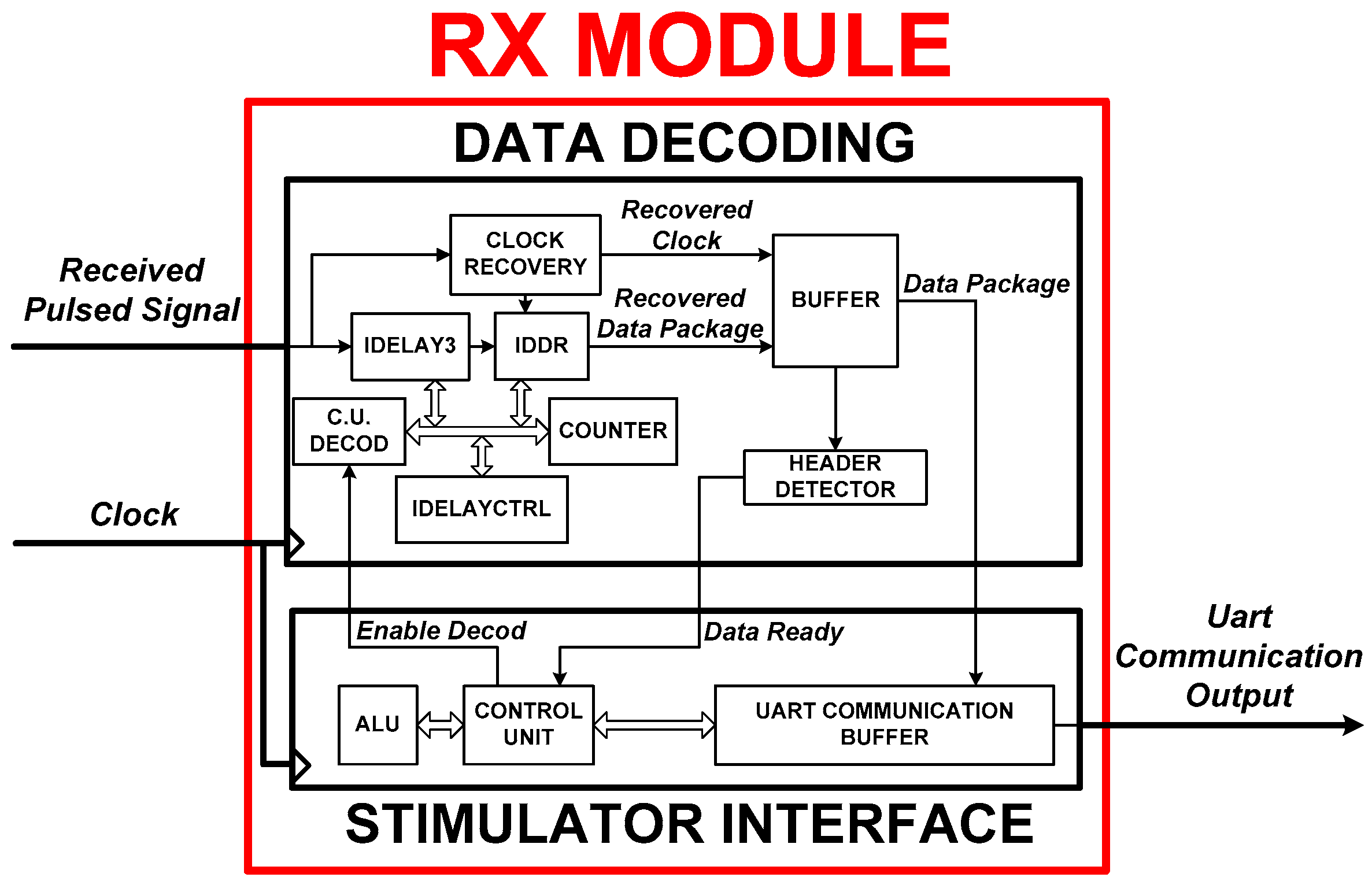
Finally, the last block in the receiver board is the RX module shown in Figure 9, implemented on a Virtex6 FPGA (ML605 by Xilinx). The main clock signal in this block is equal to 100 MHz. Starting from the received pulsed signal provided by the conditioning circuit, the clock recovery sub-block recovers and regenerates the 100 MHz clock signal starting from the received “Synchronism Pulses”. Simultaneously, the IDELAYE3 primitive block processes the same received pulsed signal to start the data recovery procedure. This is a programmable time delay line implemented into the I/O blocks of the FPGA that provides a finite and discrete time delay to be added to the input pulsed signal. As a consequence, the IDDR primitive block acquires the recovered data package starting from the data pulses, which are acquired at the falling edge of the recovered clock of the properly delayed received pulsed signal. At the starting time of the data decoding block, the control unit DECOD (C.U. DECOD) gradually increases the time delay introduced by IDELAYE3 until the rising edge of the recovered clock is in phase (i.e., synchronous) with the synchronism pulses. In this way, the falling edge of the recovered clock recovers the bit stream from the received data pulses. Furthermore, to perform compensation of the time delay variations of the IDELAYE3 due to supply voltage and/or operating temperature drifts, the C.U. DECOD properly enables and controls the IDELAYCTRL block, which is a further primitive used for this specific purpose implemented on the FPGA. The recovered data package provided by the IDDR is stored in a specific buffer (buffer) when the header sequence is correctly detected/recognized by the header detector block. Thus, the data-ready signal is set to a high logic state, indicating that the operation has been correctly performed and the data package has been acquired. At this time, the data package is sent to the stimulator interface, which suitably processes and sends it to a stimulator and/or PC monitor through a standard UART communication protocol.
In particular, the data are processed to provide proper control commands to the stimulator device together with the generation of stimuli corresponding to the touch detected by the input tactile sensors. Once the UART transmission is accomplished, the control unit of the stimulator interface block enables the decoding and acquisition of the subsequent data package with the signal named “Enable Decod”. Moreover, the control commands carry out the parameters related to the stimulations to be generated (e.g., stimulation pulse intensity, frequency and electrode channel position, etc.), which could change according to the type and force intensity of the touch of the sensing elements (i.e., corresponding to their physical stimulation).

3.4. The Electrotactile Stimulator

The WESP stimulator, fabricated by Tecnalia Serbia, is a battery-powered device that offers 24 programmable channels. The stimulator generates current pulses in the range of 0–10 mA of intensity and 1–400 Hz of frequency with a pulse width ranging from 50 ms to 500 ms. This allows the stimulator to produce electrotactile pulses with different parameter combinations. The stimulator is controlled by the stimulator interface block of the RX module. When the system detects a touch, the receiver delivers the information to the stimulator by transmitting the corresponding commands. The command orders the stimulator to generate electrotactile pulses at specific given parameters.

4. Experimental Setup and Results

The experimental setup was implemented as shown in Figure 10. It incorporated an array of 32 tactile sensors (taxels) along with the ADC interface. The TX and RX modules were implemented on two FPGA boards with the optoelectronic devices (laser driver and conditioning circuit) and circuits of the optical communication link. The overall system, operating at a 100 Mbps transmission data rate through the optical communication link, was connected to a PC through a USB cable to (i) collect the sensor data and plot them using MATLAB and (ii) display the touch information onto a graphical user interface (GUI). The GUI interface layout had the structure of the sensor array for the easy identification of the location of the touch on the screen. It is important to note that in this specific implementation used as a proof-of-concept system, the employed optical transmission data rate of 100 Mbps (i.e., 6.25 Ms/s) was oversized with respect to the sampling rate of the tactile sensor data equal to 2 ks/s. In this study, the number of employed tactile sensors was chosen arbitrarily. However, following a miniaturization/integration process of the sensor array, the achievable bandwidth of the proposed optical link will allow future studies to strongly increase the number of sensors and their typologies to control the actuators of mechanical implants through a single optical fiber-based optical link, even bidirectionally.
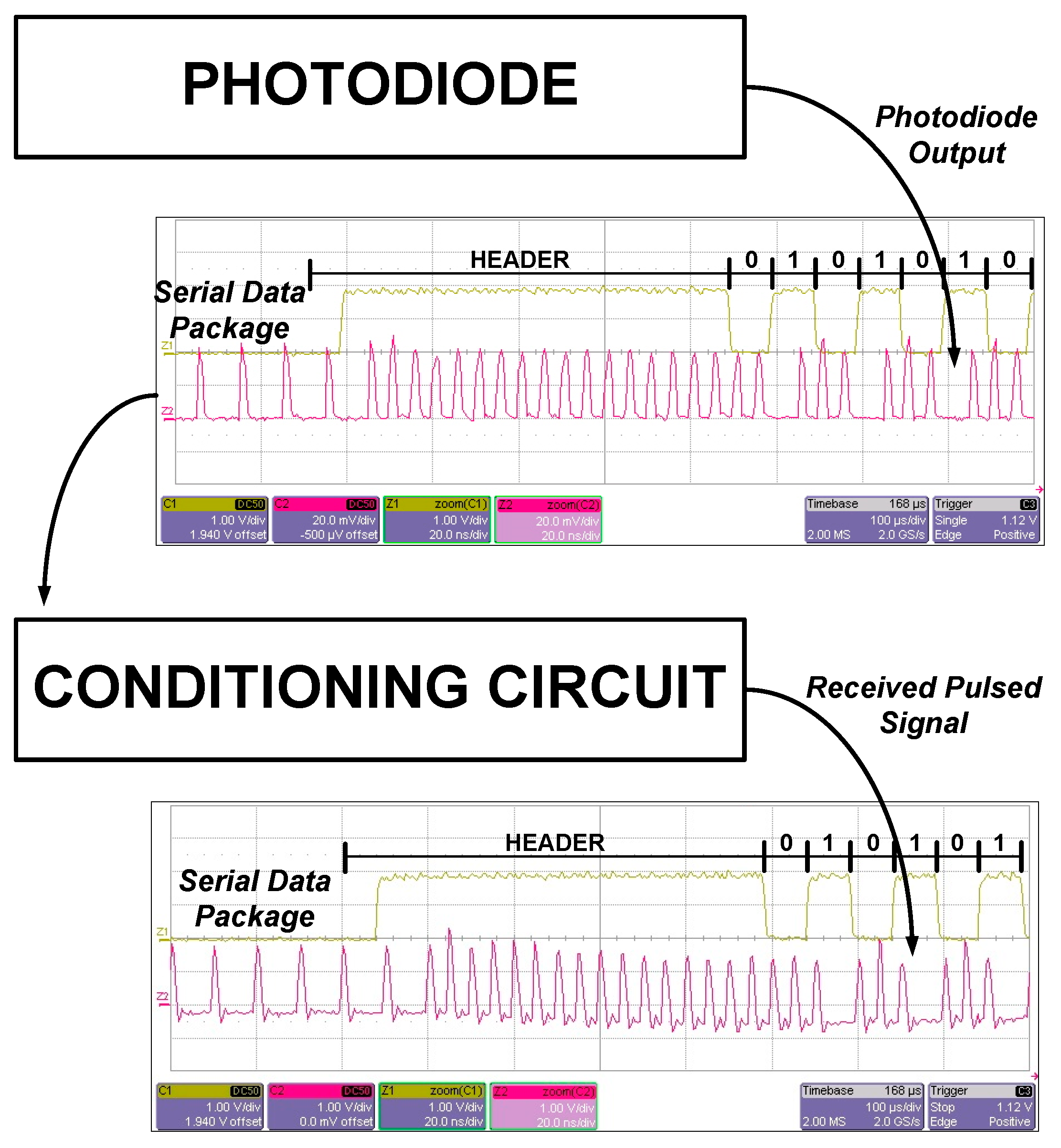
For the first validation test of the designed architecture, a package of 512 bits constructed through a repeated sequence of {0,1} bits was employed to verify the correctness of the data transmission and the overall optical communication link. All the signals were evaluated and acquired through the 6 GHz bandwidth digital oscilloscope LeCroy Master 8600A. In particular, Figure 11 shows the initial part of the transmitted bits of the serial data package, generated starting from the chosen repeated bit sequence {0,1} and the corresponding pulsed coded sequence measured at the output of the PD. In this way, it was possible to observe the correct functionality of both the data coding and laser driver blocks. In the lower part of Figure 11, it is also possible to observe the received pulsed signals generated by the conditioning circuit, which were subsequently read by the RX module. As shown, the conditioning circuit was able to correctly amplify the signal coming from the PD.
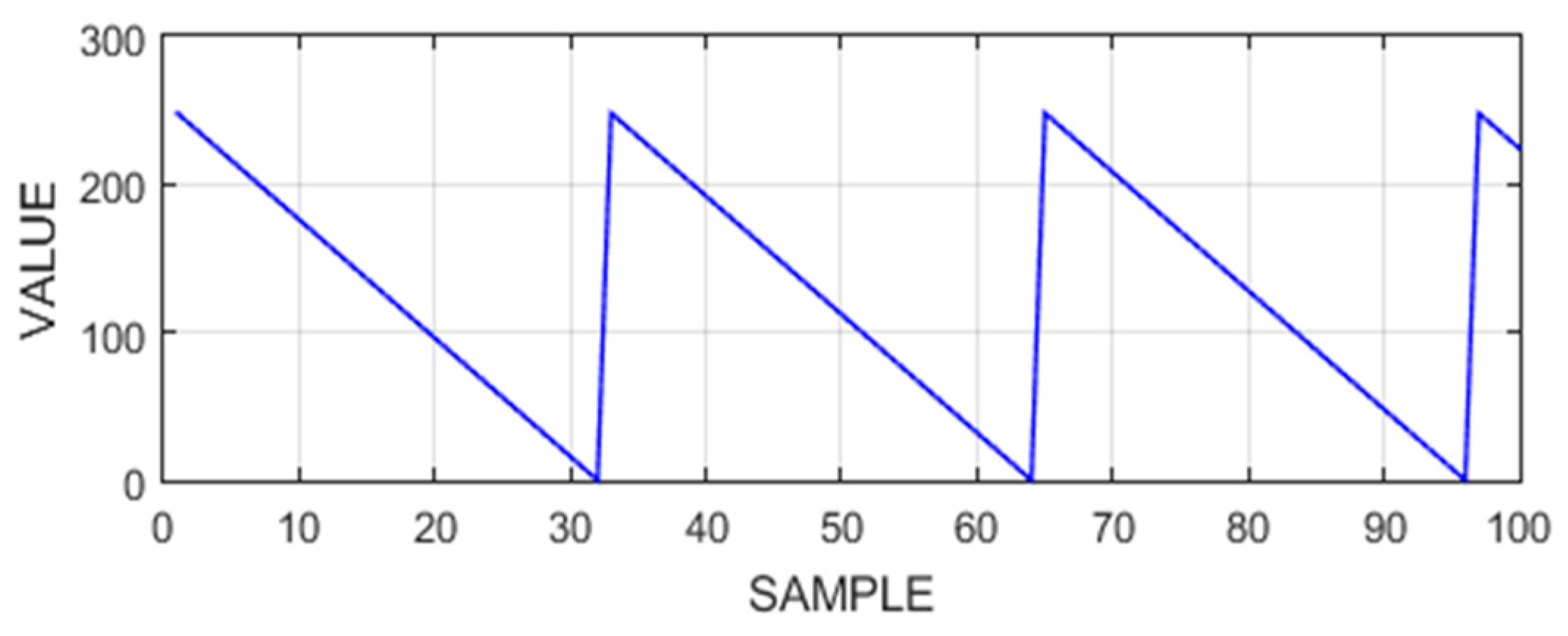
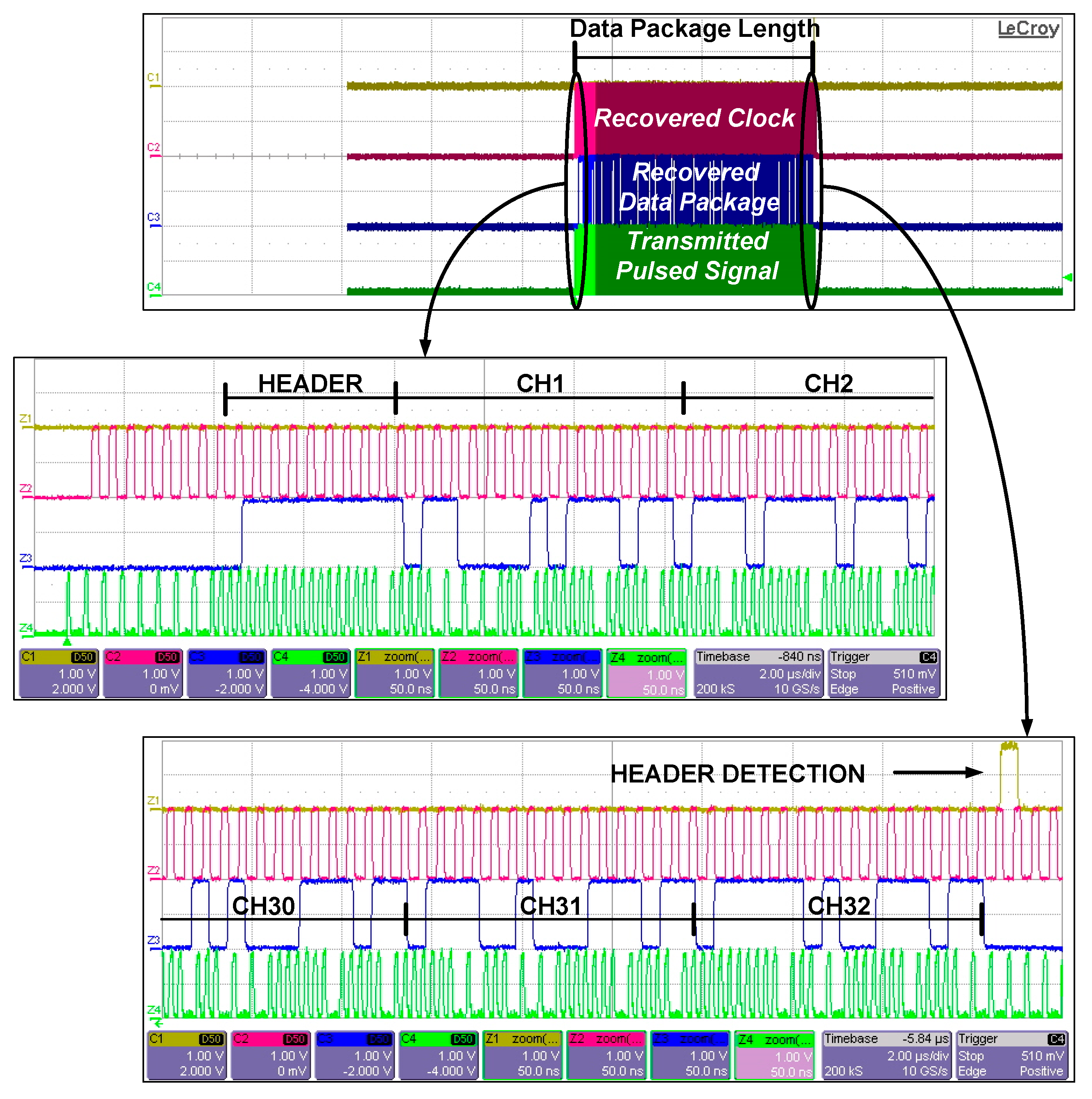
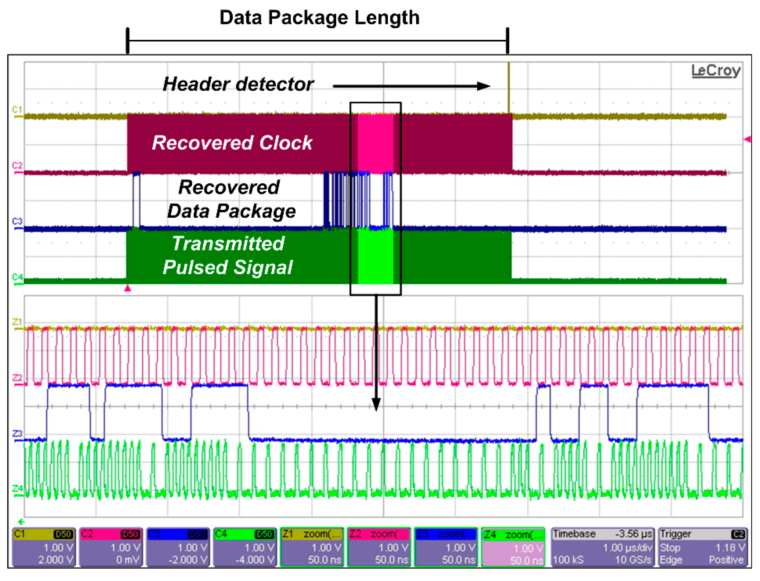
In order to evaluate the correctness of the decoding process of the transmitted serial data operated by the RX module and verify also the UART communication output, an experimental measurement has been performed using a package of 512 bits containing the samples of a ramp voltage signal, periodically sent from the transmitter to the receiver. After the data decoding and processing performed by the receiver module, the recovered data have been transmitted to the PC through a UART communication protocol, implemented into the receiver on FPGA. As shown in Figure 12, a MATLAB environment was used to acquire the received and decoded data package and plot in real-time the corresponding samples. Finally, Figure 13 and Figure 14 show an example of the measurement results achieved by testing the complete proposed system: the green channel reports the transmitted pulsed signal generated starting from the data/information coming from the tactile sensors when events occur simultaneously on each tactile sensor (see Figure 13) or only on few of them (see Figure 14) (both were digitalized and collected into the serial data package). The purple and blue channels show the clock and the data recovered by the data decoding block, respectively. Moreover, in the magnified sections of Figure 13, the header and the beginning of the serial data package are highlighted, while the lower part shows the last bits acquired and the signal that indicated the correct detection of the header. A summary of the main overall system specifications, performances and characteristics is reported in Table 1. In addition, Table 2 compares the achieved main characteristics of the proposed optical communication link with those of different state-of-the-art solutions. We note that the maximum working distance for the proposed fiber-based optical link depends on the wavelength of the employed VCSEL. Table 2 reports the maximum working distance achievable in the present case, which can be extended up to several kilometers if the system is set to operate with VCSL emitting in the 2nd or 3rd window of optical communication data links. The system is able to acquire data from 32 tactile sensors at 2 kS/s and elaborate/transmit data at 100 Mbps with a 50 pJ/bit power consumption requiring a small number of FPGA resources.

5. Conclusions

A tactile sensory feedback system based on an optical fiber communication link for prosthetic applications was described and implemented. The UWB-based pulsed data-coding technique of the optical channel allowed the system to operate at a high data rate with low power transmission. The assembled system was composed of digital transmitter and receiver blocks and an acquisition circuit that interfaced with 32 piezoelectric sensors. The transmitter acquired, encoded and sent sensor data via the optical channel, whereas the receiver decoded, recovered and translated the sensor data into commands. These commands controlled an electrotactile stimulator, conveying the tactile information to the user as electrotactile stimulations. The transmission performances were evaluated by emulating the data coming from 32 sensors sent to an external apparatus (i.e., PC and/or oscilloscope), which represented a possible stimulator. A summary of the main overall system specifications, performances and characteristics is reported in Table 1. The achieved results demonstrate the correct functionality of the proposed system and its capability to transfer a large amount of data at 100 Mbps with a power consumption 50 pJ/bit. Moreover, thanks to the higher bandwidth obtained by combining the optical link and proposed data-coding technique, a larger number of tactile sensors can be easily employed for more complex sensory feedback systems while maintaining real-time operation.

Author Contributions

A.D.M. developed the platform. He contributed to writing and editing the manuscript and coordinated the manuscript elaboration. E.P. developed the optoelectronic/photonic components and analyzed the data. He contributed to writing and supervising the manuscript. M.V. and M.F. analyzed the data results of the system contributing to theoretical discussions. They contributed to writing and editing the manuscript. G.D.P.S. and M.S. simulated, implemented and characterized the system, thus equally providing the greatest contribution to this work. They contributed to writing and editing the manuscript. A.I. supplied the overall system specifications and constraints and analyzed the data. He contributed to writing and editing the manuscript. All authors have read and agreed to the published version of the manuscript.

Funding

This work was supported by the Italian Ministry of University and Research (MUR), National Innovation Ecosystem, Recovery and Resilience National Plan (PNRR) Italy, Vitality, CUP D73C2200084000.

Conflicts of Interest

The authors declare no conflict of interest.

References

  1. Ward, K.; Pamungkas, D. Multi-channel Electro-tactile Feedback System for a Prosthetic Hand. In Mechatronics and Machine Vision in Practice 3; Billingsley, J., Brett, P., Eds.; Springer: Heidelberg, Germany, 2018; ISBN 978-3-319-76947-9. [Google Scholar]
  2. Liu, X.X.; Chai, G.H.; Qu, H.E.; Lan, N. A sensory feedback system for prosthetic hand based on evoked tactile sensation. In Proceedings of the 37th Annual Conference IEEE EMBC, Milan, Italy, 25–29 August 2015. [Google Scholar]
  3. Weiner, P.; Neef, C.; Shibata, Y.; Nakamura, Y.; Asfour, T. An Embedded, Multi-Modal Sensor System for Scalable Robotic and Prosthetic Hand Fingers. Sensors 2020, 20, 101. [Google Scholar] [CrossRef] [PubMed] [Green Version]
  4. Choi, B.; Kang, S.; Choi, H. Development of tactile sensor for detecting contact force and slip. In Proceedings of the Conference IEEE RSJ, Edmonton, Canada, 2–6 August 2005. [Google Scholar]
  5. Kostić, M.; Kojić, V.; Ičagić, S.; Andersson Ersman, P.; Mulla, M.Y.; Strandberg, J.; Herlogsson, L.; Keller, T.; Štrbac, M. Design and Development of OECT Logic Circuits for Electrical Stimulation Applications. Appl. Sci. 2022, 12, 3985. [Google Scholar] [CrossRef]
  6. Lee, H.-K.; Chang, S.-I.; Yoon, E. A Flexible Polymer Tactile Sensor: Fabrication and Modular Expandability for Large Area Deployment. J. Microelectromechanical Syst. 2006, 15, 1681–1686. [Google Scholar] [CrossRef]
  7. Weiss, K.; Worn, H. Resistive tactile sensor matrices using inter-electrode sampling. In Proceedings of the Conference IEEE IECON, Raleigh, NC, USA, 6–10 November 2005. [Google Scholar]
  8. Peng, Y.; Yang, N.; Xu, Q.; Dai, Y.; Wang, Z. Recent Advances in Flexible Tactile Sensors for Intelligent Systems. Sensors 2021, 21, 5392. [Google Scholar] [CrossRef] [PubMed]
  9. Capineri, L.; Bulletti, A. A Versatile Analog Electronic Interface for Piezoelectric Sensors Used for Impacts Detection and Positioning in Structural Health Monitoring (SHM) Systems. Electronics 2021, 10, 1047. [Google Scholar] [CrossRef]
  10. Pohtongkam, S.; Srinonchat, J. Tactile Object Recognition for Humanoid Robots Using New Designed Piezoresistive Tactile Sensor and DCNN. Sensors 2021, 21, 6024. [Google Scholar] [CrossRef] [PubMed]
  11. Bulić, P.; Kojek, G.; Biasizzo, A. Data Transmission Efficiency in Bluetooth Low Energy Versions. Sensors 2019, 19, 3746. [Google Scholar] [CrossRef] [PubMed] [Green Version]
  12. Mikhaylov, K.; Tervonen, J. Evaluation of Power Efficiency for Digital Serial Interfaces of Microcontrollers. In Proceedings of the Conference IEEE NTMS, Istanbul, Turkey, 7–10 May 2012. [Google Scholar]
  13. De Marcellis, A.; Di Patrizio Stanchieri, G.; Palange, E.; Faccio, M.; Constandinou, T.G. An Ultra-Wideband-Inspired Systemon-Chip for an Optical Bidirectional Transcutaneous Biotelemetry. In Proceedings of the Conference IEEE BioCAS, Cleveland, OH, USA, 17–19 October 2018. [Google Scholar]
  14. De Marcellis, A.; Di Patrizio Stanchieri, G.; Faccio, M.; Palange, E.; Constandinou, T. A 300 Mbps 37 pJ/bit UWB-Based Transcutaneous Optical Biotelemetry Link. IEEE Trans. BIOCAS 2020, 14, 441–451. [Google Scholar] [CrossRef] [PubMed]
  15. Di Patrizio Stanchieri, G.; Saleh, M.; Sciulli, M.; De Marcellis, A.; Ibrahim, A.; Valle, M.; Faccio, M.; Palange, E. FPGA-Based Tactile Sensory Feedback System with Optical Fiber Data Communication Link for Prosthetic Applications. In Proceedings of the Conference IEEE ICECS, Genoa, Italy, 27–29 November 2019. [Google Scholar]
  16. Bianchi, M.; Haschke, R.; Büscher, G.; Ciotti, S.; Carbonaro, N.; Tognetti, A. A Multi-Modal Sensing Glove for Human Manual-Interaction Studies. Electronics 2016, 5, 42. [Google Scholar] [CrossRef]
  17. Vidal-Verdú, F.; Barquero, M.J.; Castellanos-Ramos, J.; Navas-González, R.; Sánchez, J.A.; Serón, J.; García-Cerezo, A. A Large Area Tactile Sensor Patch Based on Commercial Force Sensors. Sensors 2011, 11, 5489–5507. [Google Scholar] [CrossRef] [PubMed] [Green Version]
  18. Schmitz, A.; Maiolino, P.; Maggiali, M.; Natale, L.; Cannata, G.; Metta, G. Methods and Technologies for the Implementation of Large-Scale Robot Tactile Sensors. IEEE Trans. Robot. 2011, 27, 389–400. [Google Scholar] [CrossRef]
  19. Huang, H.; Li, T.; Bruschini, C.; Enz, C.; Justiz, J.; Antfolk, C. Multi-modal Sensory Feedback System for Upper Limb Amputees. In Proceedings of the Conference IEEE NGCAS, Genova, Italy, 6–9 September 2017. [Google Scholar]
  20. Saleh, M.; Ibrahim, A.; Ansovini, F.; Mohanna, Y.; Valle, M. Low Power Electronic System for Tactile Sensory Feedback for Prosthetics. J. Low Power Electron. 2019, 15, 95–103. [Google Scholar] [CrossRef]
  21. Schmitz, J.A.; Sherman, J.M.; Hansen, S.; Murray, S.J.; Balkir, S.; Hoffman, M.W. A Low-Power, Single-Chip Electronic Skin Interface for Prosthetic Applications. IEEE Trans. Biomed. Circuits Syst. 2019, 13, 1186–1200. [Google Scholar] [CrossRef] [PubMed]
  22. Abbass, Y.; Saleh, M.; Dosen, S.; Valle, M. Embedded Electrotactile Feedback System for Hand Prostheses Using Matrix Electrode and Electronic Skin. IEEE Trans. Biomed. Circuits Syst. 2021, 15, 912–925. [Google Scholar] [CrossRef]
  23. Abbass, Y.; Dosen, S.; Seminara, L.; Valle, M. Full-hand electrotactile feedback using electronic skin and matrix electrodes for high-bandwidth human-machine interfacing. Philos. Trans. R. Soc. A Math. Phys. Eng. Sci. 2022, 380, 2228. [Google Scholar] [CrossRef]
  24. Javan-Khoshkholgh, A.; Farajidavar, A. An Implantable Inductive Near-Field Communication System with 64 Channels for Acquisition of Gastrointestinal Bioelectrical Activity. Sensors 2019, 19, 2810. [Google Scholar] [CrossRef] [PubMed] [Green Version]
  25. Stoecklin, S.; Rosch, E.; Yousaf, A.; Reindl, L. Very High Bit Rate Near Field Communication with Low-Interference Coils and Digital Single-Bit Sampling Transceivers for Biomedical Sensor Systems. Sensors 2020, 21, 6025. [Google Scholar] [CrossRef] [PubMed]
  26. Seminara, L.; Capurro, M.; Cirillo, P.; Cannata, G.; Valle, M. Electromechanical characterization of piezoelectric PVDF polymer films for tactile sensors in robotics applications. Sens. Actuators A Phys. 2011, 169, 49–58. [Google Scholar] [CrossRef]
  27. Zirkl, M.; Sawatdee, A.; Helbig, U.; Krause, M.; Scheipl, G.; Kraker, E.; Ersman, P.A.; Nilsson, D.; Platt, D.; Bodö, P.; et al. An All-Printed Ferroelectric Active Matrix Sensor Network Based on Only Five Functional Materials Forming a Touchless Control Interface. Adv. Mater. 2011, 23, 2069–2074. [Google Scholar] [CrossRef] [PubMed]
  28. Fares, H.; Abbass, Y.; Valle, M.; Seminara, L. Validation of Screen-Printed Electronic Skin Based on Piezoelectric Polymer Sensors. Sensors 2020, 20, 1160. [Google Scholar] [CrossRef] [PubMed] [Green Version]
  29. 32-Channel, Current-Input Analog-to-Digital Converter. Available online: www.ti.com (accessed on 2 May 2019).
Figure 1. Block diagram of the overall proposed system.
Electronics 12 00627 g001
Figure 2. Block diagram of the data acquisition system: (a) offset circuit; (b) current-input analog-to-digital converter (DDC232 commercial device).
Electronics 12 00627 g002
Figure 3. Block scheme of the optical communication link.
Electronics 12 00627 g003
Figure 4. Example of the timing diagram of the optical UWB-based pulsed data-coding technique.
Electronics 12 00627 g004
Figure 5. Block scheme of the TX MODULE.
Electronics 12 00627 g005
Figure 6. Structure/composition of the serial data package.
Electronics 12 00627 g006
Figure 7. Schematic circuit of the laser driver.
Electronics 12 00627 g007
Figure 8. Schematic circuit of the conditioning circuit.
Electronics 12 00627 g008
Figure 9. Block scheme of the RX module.
Electronics 12 00627 g009
Figure 10. Photo of the experimental set-up showing the two FPGA boards and the optical communication link composed of the optoelectronic devices and circuits together with the optical fiber.
Electronics 12 00627 g010
Figure 11. Experimental measurement: serial data package related to a repeated {0,1} bit serial sequence and the subsequent transmitted pulsed signal operating at 100 Mbps. The transmitted pulsed signal was observed at the output of the PD and the conditioning circuit (i.e., received pulsed signal).
Electronics 12 00627 g011
Figure 12. Example of samples of a periodic ramp voltage signal that has been coded, transmitted via optical fiber, decoded, sent to a PC through a UART communication protocol (implemented in the RX module on FPGA) and plotted in a MATLAB environment.
Electronics 12 00627 g012
Figure 13. Experimental measurement of the overall system operating at 100 Mbps when events occur simultaneously on each tactile sensor: the green channel is the transmitted pulsed signal related to the data coming from the tactile sensors; the purple and blue channels are the recovered clock and recovered data package, respectively; the yellow channel is the detection signal of the header.
Electronics 12 00627 g013
Figure 14. Experimental measurement of the overall system operating at 100 Mbps when events occur on few tactile sensors: the green channel is the transmitted pulsed signal related to the data coming from the tactile sensors; the purple and blue channels are the recovered clock and recovered data package, respectively; the yellow channel is the detection signal of the header.
Electronics 12 00627 g014
Table 1. Main Proposed tactile sensory feedback system: main specifications, performances and characteristics.
Number of tactile sensors32
Sensor data sampling rate2 kS/s
Optical transmission data rate100 Mbps
Optical link power consumption5 mW
Transmission power efficiency50 pJ/bit
FPGA LUTs for the Tx + Rx1420 + 1320
FPGA FFs for the Tx + Rx2230 + 2860
Table 2. Comparison of the main characteristics of the optical data link with those of the state-of-the-art.
[Ref]
Year
[22]
2019
[24]
2019
[25]
2020
[This Work]
2023
Data rate [Mbps]10.1256.78100
Efficiency [pJ/bit]30 k50.4 k1.01 k50
Communication linkBluetoothRFIDInductiveOptical
Maximum operating distance [m]<1000.050.01200
Disclaimer/Publisher’s Note: The statements, opinions and data contained in all publications are solely those of the individual author(s) and contributor(s) and not of MDPI and/or the editor(s). MDPI and/or the editor(s) disclaim responsibility for any injury to people or property resulting from any ideas, methods, instructions or products referred to in the content.