3.1. Description of the Experimental Prototype
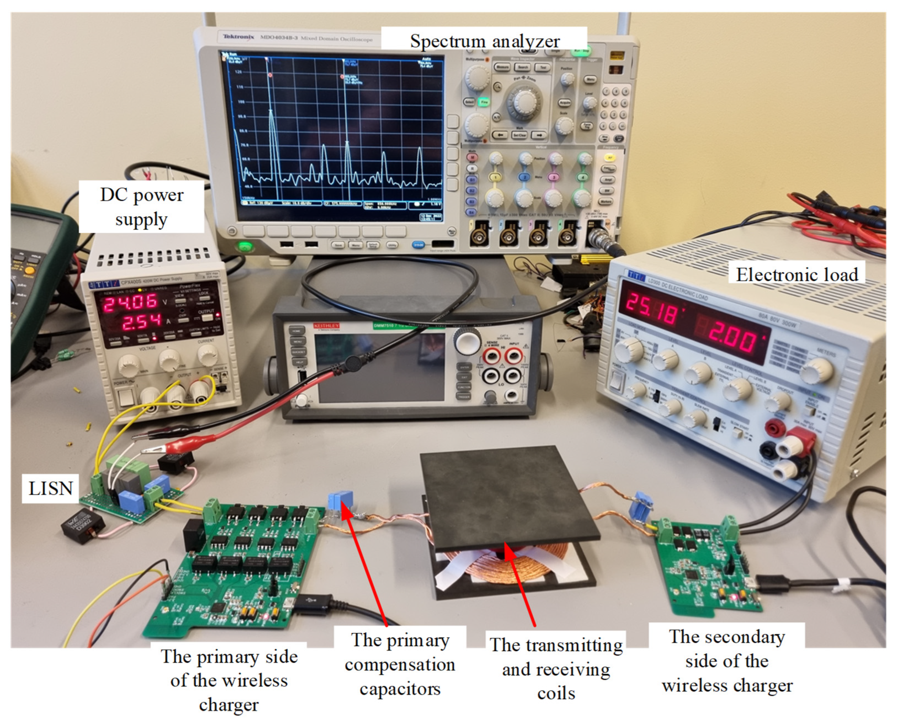
For the experimental studies, a scaled-down 50 W laboratory prototype of a wireless battery charger was designed and physically built. The prototype together with the measurement equipment is demonstrated in
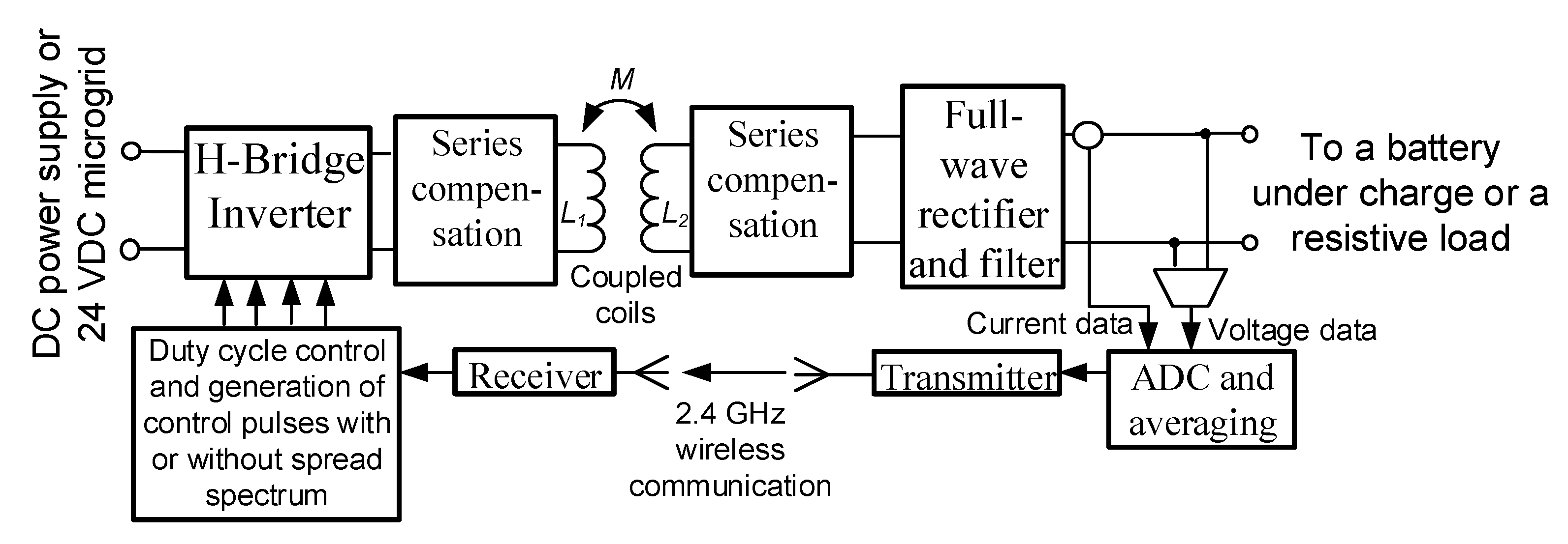
Figure 2. A block diagram and simplified schematic diagram of the designed wireless battery charger are depicted in
Figure 3 and
Figure 4, respectively.
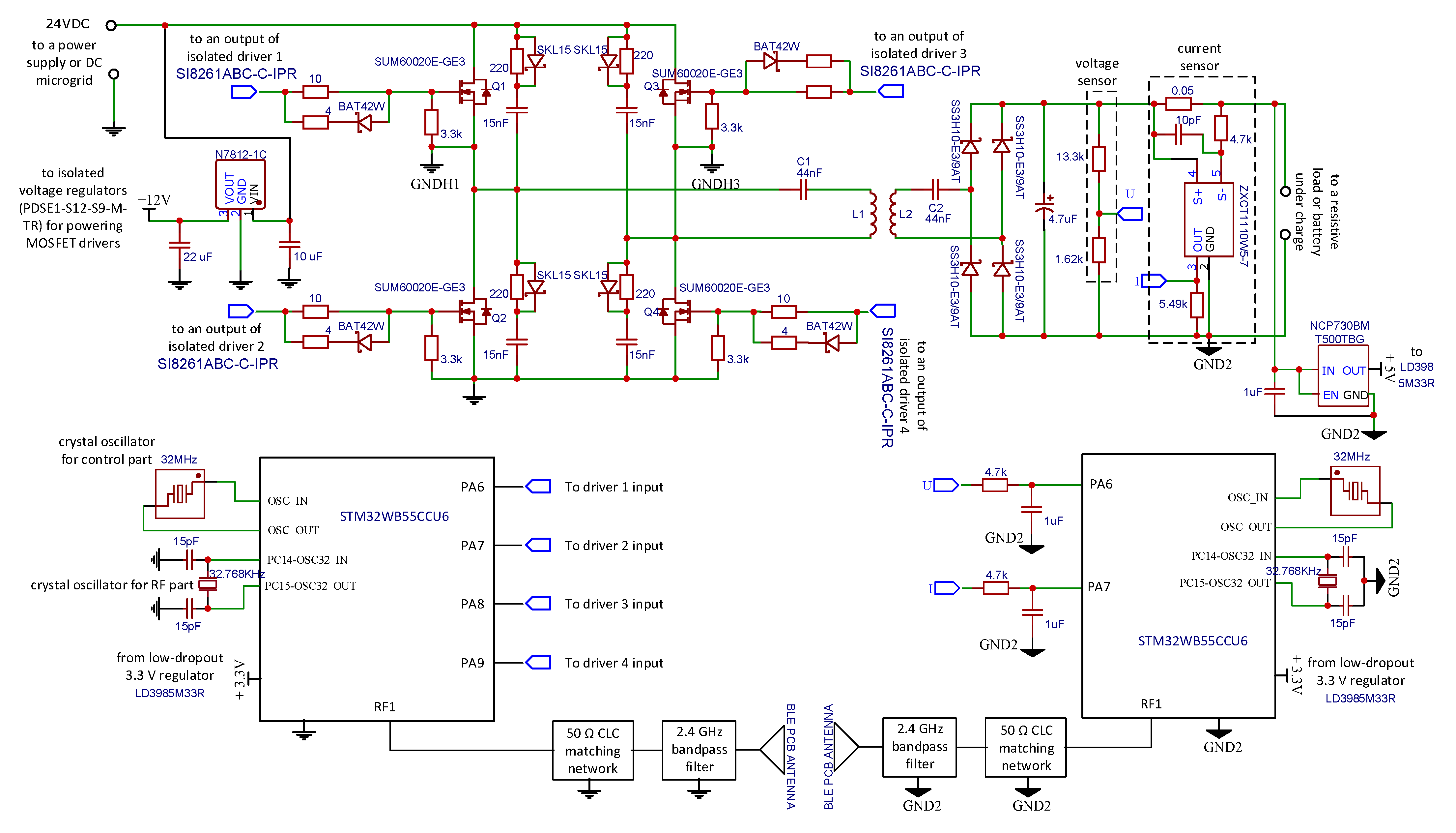
The designed wireless battery charger primary side has an H-bridge inverter (with four surface-mount transistors having low-drain-to-source resistance), four RCD snubber circuits, four isolated MOSFET drivers (with some auxiliary external components), two polymer film capacitors connected in parallel (with low equivalent series resistance) for the series compensation, four isolated step-down switch-mode power converters (with same external components) for powering the drivers, one switch-mode step-down converter to convert input voltage 24 V to output voltage 12 V, a relatively inexpensive microcontroller (with internal transceiver circuit) STM32WB55CCU6, with some external components (e.g., crystal oscillators), the transmitting coil L1 and PCB antenna (
Figure 4). The secondary side of the charger is more compact, and it has the receiving coil L2, two polymer film capacitors connected in parallel (for the series compensation), full-wave rectifier with Schottky diodes followed by the filtering capacitor, as well as current and voltage sensors. The control part of the secondary side is represented by the same microcontroller (with some external components) as in the primary side and PCB antenna. The secondary-side microcontroller is necessary to: (1) gather data from the output sensors every 10 ms; (2) make analog to digital conversion; (3) average a set of ten measurement results; (4) prepare data for the transmission; (5) generate a modulated 2.4 GHz signal for Bluetooth low energy (BLE) communications. The primary side microcontroller receives the data due to the wireless communication link between it and the secondary-side microcontroller, and then, the primary-side microcontroller completes the following actions: it computes the duty cycle of the MOSFETs control signals (by using digital PID controller), and it generates four square pulses with definite duty cycles to control the MOSFETs and to regulate the charger output voltage or current. In addition, the primary side microcontroller is necessary to toggle from COC to COV mode (if the output voltage is equal to cut-off charge voltage 25.2 V), to switch-off the charging process if the output current < 200 mA and to implement the multi-switching frequency technique with different parameters. A suitable code is recorded to a memory of the microcontrollers to implement COC or COV modes and the multi-switching-frequency schemes.
The wireless charger specifications are presented in
Table 1. It can be applied to small mobile robots for 6-cell Li-ion or Li-polymer battery charging under COC mode followed by COV mode. The designed prototype can allow us to study the effect of different parameters of the multi-switching-frequency technique on the performance characteristics of the wireless battery charger and to compare the results to the performance characteristics of the conventional wireless charger without the spread-spectrum techniques.
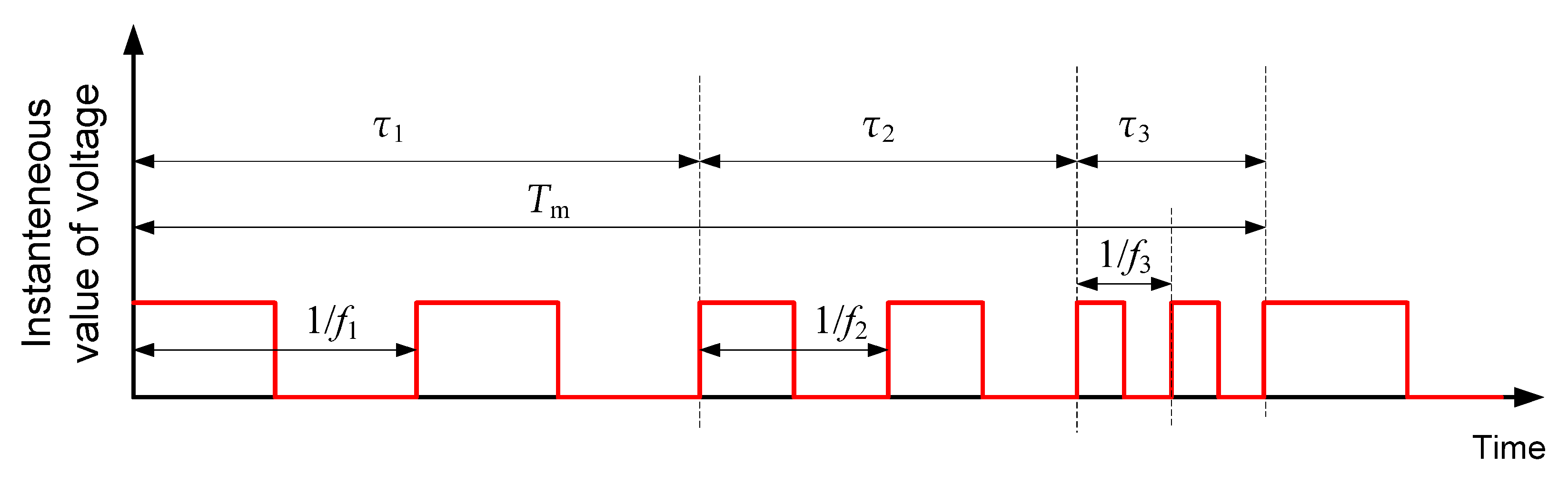
The operating frequencies for the multi-switching frequency technique can be chosen within the Qi-standard-allowed range of frequencies. As DC input voltage, the voltage of 24 V is chosen, because of the high popularity of 24 V DC microgrids. The resonant frequency (frez) of the primary resonant tank was approximately 150 kHz. The switching frequency of the charger without the spread spectrum or the second frequency f2 of the charger with the three-switching frequency scheme was equal to frez approximately. Since the input equivalent resistance of a battery under charge increases from 11.1 to 126 Ω, instead of the battery, we used an electronic load LD300 in constant resistance mode. The range of the load resistances 11.1–12.6 Ω corresponds to COC, but the range of the resistances 12.6–126 Ω corresponds to COV. The boundary resistance between COC and COV is 12.6 Ω.
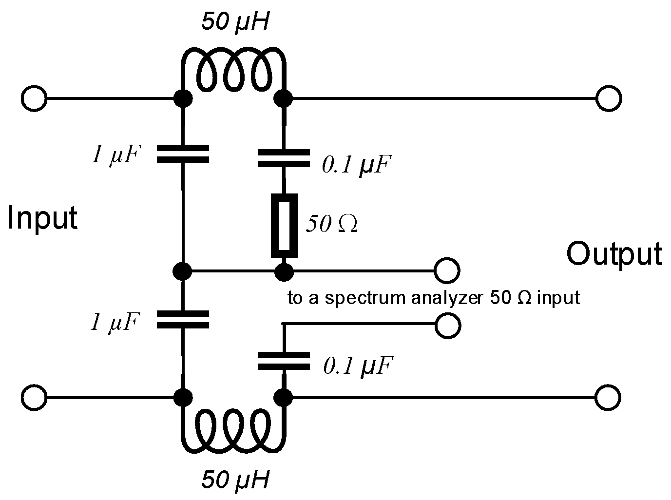
In the conducted emissions measurements, we used home-made LISN (
Figure 2), the schematic diagram (
Figure 5) of which corresponds to a simplified version of a factory-made LISN with CISPR specifications. During the efficiency (
η) measurements, LISN was disconnected from the circuit. The conducted emissions spectrum (at the high-frequency output of LISN) was analyzed in the frequency domain according to the requirements of the international standard CISPR11: the measurement frequency range 0.15 MHz –30 MHz; resolution bandwidth (RBW) 9 kHz. For the conducted emissions measurements, a mixed domain oscilloscope Tektronix MDO4034B with a built-in spectrum analyzer (with a peak detector) was used. For the primary coil current measurements, a wide-bandwidth current probe Tektronix was used.
3.2. Design of the Experimental Prototype
In this subsection, it will be shown how the main circuit components were chosen. In the calculations, it is assumed that there are no losses in the circuit; the resonant tank currents are sine, and maximum RMS values of currents of the power components are at the boundary between COC and COV modes (load resistance Rload = 12.6 Ω).
Initially, we should know the values of inductances of the receiving and transmitting coils (L1 and L2, respectively). We used Ansys Maxwell computational electromagnetics software to model the coils at different distances and misalignments. The following assumptions were made during the modeling: the ferrite pad is KEMET FPL100 (100 × 100 × 4 mm; relative magnetic permeability 3000 and saturation field 520 mT); the coils outer diameter is 84 mm; the coils inner diameter is 55 mm; there is only single layer of copper wire. The modeling results showed: the inductances of the coils are 27 µH at the rated distance of 2.8 cm (the coils are aligned perfectly); the mutual inductance M between the coils is 9 µH at the rated distance between the coils (the coils are aligned perfectly); M = 8.25 µH (with the maximum misalignment of 1 cm).
In order to choose litz wire for the transmitting coil, the RMS value of the coil current must be calculated using the following expression [
17]:
where
is the referred impedance from the secondary side to the primary side of the WPT system,
[
17];
is the equivalent load resistance,
[
18] (
is the load resistance);
is the inverter output voltage fundamental harmonic RMS value,
[
18].
Assuming that the maximum RMS value of the transmitting coil current is at the worst-coupling case (M = 8.25 µH) and when Rload corresponds to the boundary between COC and COV modes (Rload in this case equals 12.6 Ω), we calculated using (1) that = 2.92 A; = 10.22 Ω; = 5.9 Ω; = 17.21 V. Considering that = 2.92 A, we choose litz wire CLI 200/120 (120 strands; effective cross section area of 0.943 mm2), which can sustain AC currents with RMS values up to 3.36 A. Note that the calculations are made assuming that the charger operates at a single frequency f = 150 kHz, and if the charger operates at three different frequencies, RMS value of the current may increase. However, as is shown in simulations of the charger in the PSIM software, the increase in the RMS value is relatively low (few% only) and, therefore, litz wire CLI 200/120 can be used even if there is a spread spectrum. After calculating peak magnetic field density in the coil L1 ferrite pad (for the worst-case coupling), it was concluded that it is well below the saturation field of the ferrite pad KEMET FPL100. Simulations of the charger circuit in the PSIM software showed that the multi-switching-frequency scheme can increase the peak value of the coil L1 current by up to 30%, but the selected ferrite will not be saturated because of its relatively large saturation field.
In order to choose a litz wire for the receiving coil, the RMS value of the coil current must be calculated using the following expression [
18]:
where
is the charger output DC current. Assuming that the maximum value of
= 2 A is in COC mode, it can be calculated that
= 2.21 A. Thus, as a litz wire and ferrite pad, we can use CLI 200/120 and KEMET FPL100, respectively.
Capacitances of the compensation capacitors C1 and C2 can be calculated using the well-known Thomson formula as follows:
In order to choose correct capacitors, we should know peak voltage across them and the current RMS value. It is obvious that the total current RMS value through C1 is
= 2.92 A, but the total current RMS value through C2 is
= 2.21 A. Taking into account that a waveform of the currents through the capacitors is sine, peak voltages across the capacitors may be calculated using the following expressions:
Calculating for the worst-case coupling, we can obtain from (5) and (6) that = 104.7 V and = 79.24 V. Thus, (5) and (6) are valid only for operation at single-switching frequency. If a multi-switching-frequency scheme is used, then peak values of the voltages may increase. As the simulations in PSIM show, the peak values increase up to 30%. This will be taken into account when choosing the capacitors. Therefore, for C1 (and C2), we used two 22 nF ± 10% polymer film capacitors connected in parallel. Each capacitor has a current rating of 2 A and maximum allowable voltage of 200 V.
In order to choose correct rectifying diodes of the diode bridge at the receiving side, we should know each diode reverse voltage peak value (VDrev) and forward average current (Ifavg) at the worst case coupling and maximum output DC voltage in COC mode (Rload = 12.6 Ω). It is obvious that VDrev for each rectifying diode is equal to the output DC voltage 25.2 V approximately, but Ifavg is two times lower than output DC current (2 A) in COC mode. Thus, for the diode bridge at the receiving side, we used SS3H10-E3/9AT Schotky diodes with maximum allowable forward average current of 3 A and maximum allowable peak reverse voltage of 100 V.
In order to choose correct H-bridge transistors (Q1–Q4) at the transmitting side, we should know each transistor drain-to-source voltage peak value (
Vds) and drain current RMS value (
ITrms) at the worst-case coupling and maximum output DC voltage in COC mode (
Rload = 12.6 Ω). Assuming that the parasitic spike voltage (
Vspike) between the drain and source terminals of each transistor will be equal to the input voltage, total
Vds will be
Vin +
Vspike = 48 V. The snubber circuits (see
Figure 4) should be designed to limit the spike voltage to 24 V. The maximum value of the drain current, if Q1 and Q4 are on during one half a period, and Q2 and Q3 are one on within another half a period, will be:
Thus, for the H-bridge inverter, we used four SUM60020E low-on-resistance Si MOSFETs with maximum allowable drain-to-source voltage of 80 V and sufficient maximum allowable drain current RMS value. After making thermal calculations, we concluded that the MOSFETs can be mounted on the copper pads with a minimum recommended pad area (in their data sheet).
The external components of the current sensor, both microcontrollers and the drivers were chosen according to recommendations presented in their data sheets [
19,
20].


