Article

Thorough Study of Multi-Switching-Frequency-Based Spread-Spectrum Technique for Suppression of Conducted Emissions from Wireless Battery Chargers

Institute of Industrial Electronics and Electrical Engineering, Riga Technical University, 12/1 Azenes Street, LV-1048 Riga, Latvia
*
Author to whom correspondence should be addressed.
Electronics 2023, 12(3), 687; https://doi.org/10.3390/electronics12030687
Submission received: 30 December 2022 / Revised: 26 January 2023 / Accepted: 27 January 2023 / Published: 30 January 2023

Abstract

:
The multi-switching-frequency technique is one of the spread-spectrum techniques for suppression of conducted emissions generated by wireless battery chargers. Its advantage is a relatively easy implementation with a microcontroller. In this paper, an original thorough experimental study of the effect of the multi-switching-frequency-based spread spectrum technique parameters (e.g., combinations of number of pulses, frequency order, etc.) on the performance characteristics (conducted emissions levels, efficiency, etc.) of an inductive-resonant wireless battery charger with a closed loop control is presented. It is shown that combinations of a number of pulses and frequency order have a noticeable impact on the performance characteristics of the wireless chargers. The suppression of the conducted emissions can be improved significantly by using optimized parameters of the technique. Moreover, it is proved experimentally that a relatively inexpensive microcontroller with a transceiver can be used to implement both closed-loop control of the wireless charger and the multi-switching-frequency technique.

1. Introduction

Currently, with an enormous development of electrical and electronic technologies, the need for the wireless power transfer (WPT) has become topical due to inherent convenience and reliability of the power transfer approach. WPT has a variety of applications ranging from low-power applications (e.g., WPT to wireless sensors in wireless sensor networks) to high-power ones (e.g., wireless charging of batteries of electrical vehicles) [1]. Definitely, one of the most important applications of WPT is wireless charging of batteries of mobile robots, because of no sparking (very important for chemical warehouses), no contact wearing problems (and hence, better reliability), simple automation of charging process (very important for mobile robots), no need for high-accuracy positioning of mobile robots (because charging process will be smooth even if the charging coils are not aligned accurately), and other reasons [2,3,4]. Different types of WPT exist, but an inductive-resonant approach is the most suitable for applications such as battery charging of mobile robots, electrical vehicles, etc. Inductive-resonant wireless battery chargers can be regarded as a specific type of inductive-resonant WPT system with specific modes of operation, such as constant output current (COC) or constant output voltage (COV) modes.
Inductive-resonant wireless chargers include switch-mode power converters for power conversion, such as inverters at the primary side of the chargers. Due to the switch-mode nature of the converters, the wireless chargers generate appreciable electromagnetic emissions—conducted and radiated emissions [5,6,7]. The conducted emissions can be very problematic for sensitive electronic devices connected to the same electric grid as the wireless chargers. The radiated emissions can disrupt normal functioning of sensitive electronic devices placed nearby the inductive-resonant wireless charger or can be hazardous to humans. Therefore, various national or international electromagnetic compatibility standards, such as CISPR11, specify the limits and measurement methods of electromagnetic emissions of wireless battery chargers.
Classical approaches for conducted emissions reduction to meet the international standard requirements are passive or active filters. Passive filters increase the size, cost and weight of wireless chargers’ primary side as well as can decrease their efficiency [8]. Active filters may have lower size and weight than passive ones (especially at high power levels), but they may have stability issues and more complex design [9]. In order to reduce size and cost of the passive filters or even eliminate them, an interesting and useful approach called the spread spectrum was adapted from communication engineering and applied to conventional switch-mode power converters last decade [10]. Recently, the approach was also applied to inductive-resonant wireless battery chargers for reducing conducted and radiated emissions [11,12,13,14,15,16]. Spreading the spectrum of the conducted emissions of the wireless chargers can be achieved by different approaches, such as switching frequency modulation [5,13,16], simultaneous switching frequency and duty cycle modulation (also known as the hybrid modulation) [11], multi-switching frequency technique [12] or even multi-frequency-multi-duty-cycle approach [15]. In contrast with the passive or active filters, the spread spectrum approach does not increase the size, weight or cost of inductive-resonant WPT systems because it can be implemented by using, for instance, a microcontroller with a suitable code. Classical periodic switching frequency modulation, the hybrid modulation and the multi-frequency-multi-duty-cycle technique may require large memory and computational resources from microcontrollers used in closed-loop wireless battery chargers; therefore, less memory and computational resources consuming the spread-spectrum approach (multi-switching frequency technique) was applied to wireless battery chargers in [12]. The multi-switching-frequency technique (based on more than two frequencies) proposed in [12] was a development of an idea presented in [10] where the two-switching-frequency technique (also known as “the bi-frequency modulation”) as a specific type of multi-switching-frequency technique was applied to resonant dc/dc converters (with analog control) for the reduction of the conducted emissions. It was suggested without experimental verification in [12] that, in contrast with the other spread spectrum approaches, it could be implemented in closed-loop wireless chargers even using relatively cheap microcontrollers.
Despite the fact that the multi-switching-frequency-based spread spectrum technique for wireless battery chargers was studied in [12], the study had numerous drawbacks: (1) it was applied to wireless battery chargers operating in constant output current mode only; (2) the study was a simulation without any experimental verifications; (3) the study was not thorough because the effect of some important parameters (combinations of number of pulses and frequency order) of the multi-switching-frequency scheme on the performance characteristics of the closed-loop wireless charger was not performed; (4) the idea that relatively inexpensive microcontrollers with transceivers can be used to implement this technique together with the closed-loop control of the wireless charger with full-bridge inverters was not proved experimentally.
This paper is a continuation of our studies presented in [12], and it overcomes the aforementioned drawbacks. The following can be considered as novelty of this paper: (1) an original thorough analysis of the effect of the multi-switching-frequency scheme on the performance characteristics (e.g., conducted emissions levels, efficiency, peak and root-mean square (RMS) values of power components currents) of wireless battery chargers under constant current and constant voltage modes is completed experimentally; (2) for the first time, it is shown that combinations of a number of pulses and frequency order have a noticeable impact on the performance characteristics of wireless chargers; (3) the suppression of conducted emissions is improved significantly by using optimized parameters of the multi-switching-frequency technique; (4) for the first time, a relatively inexpensive microcontroller with a transceiver is used to implement both closed-loop control of the wireless charger and the multi-switching-frequency technique; (5) the volume of the primary side of the inductive-resonant wireless charger is reduced noticeably without degrading efficiency in COC mode and with noticeable improvement of efficiency in COV mode, if optimized parameters of the multi-switching-frequency technique are used.

2. The Multi-Switching-Frequency Technique

2.1. Parameters of the Multi-Switching-Frequency Technique

A control signal of a single transistor of a wireless battery charger inverter when the multi-switching-frequency (three-switching-frequency) technique is used is depicted in Figure 1. As it is seen in the table, the main parameters of the technique are: (1) number (F) of frequencies (f1, f2, etc.) at which the inverter operates; (2) modulation period Tm or modulation frequency fm; (3) the k-th switching frequency (f1, f2, etc.); (4) time intervals τk within which the inverter operates at the switching frequency fk; (5) the whole number (Nk) of pulses for each time interval τk; (6) the order of the switching frequencies (e.g., from low to high or from high to low) for three or more switching frequency schemes; (7) the k-th duty cycle (d1, d2, etc.).

2.2. Classical Versus Modified Multi-Switching-Frequency Technique

In the classical multi-switching-frequency techniques, N1 = N2 = Nk, but τ1τ2τk [15] or τ1 = τ2 = τk and Nk depends on τk [12]. The switching frequencies fk change from low to high, and d1 = d2 = dk in both classical cases. In order to improve the conducted emission reduction in open-loop WPT systems, the modified multi-switching-frequency technique (also known as multi-switching-frequency-multi-duty-cycle technique) was proposed in [15]. In the modified technique, the k-th duty cycle values are not equal (d1d2d3), but N1 = N2 = N3, τ1τ2τk, and the frequency order is from low to high. Despite the fact that the modified technique [15] showed better performance in the open-loop WPT systems, its implementation in closed-loop WPT systems used for wireless battery charging would be more challenging, because the output voltage or current of the wireless battery charger can be changed through a variation of the average duty cycle of the inverter. As a result, the technique will require more computational and memory resources from a microcontroller that would prevent the use of relatively inexpensive microcontrollers with transceivers in the wireless battery chargers with closed-loop control. Therefore, in this paper, we will make a thorough analysis of the effect of different parameters of the classical multi-switching-frequency scheme (when d1 = d2 = dk) on the performance of the wireless chargers and show that the classical multi-switching-frequency technique with optimized parameters gives a better conducted emission reduction than that of non-optimized classical multi-switching-frequency technique. To the contrary, the optimized technique can be easily implemented by using a relatively inexpensive microcontroller with a transceiver in a closed-loop wireless battery charger when compared to the modified multi-switching-frequency technique (multi-switching-frequency-multi-duty-cycle technique).

3. Experimental Setup

3.1. Description of the Experimental Prototype

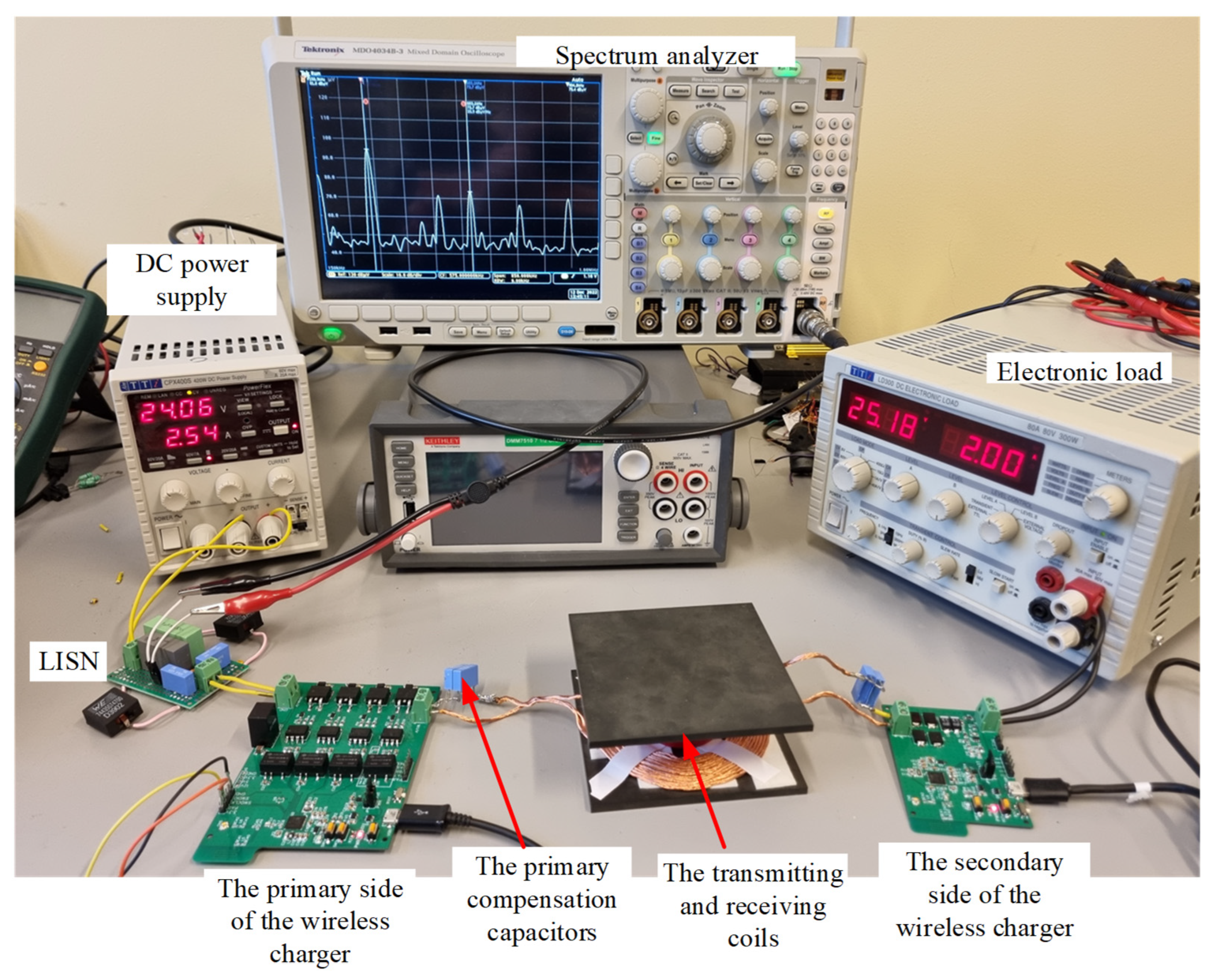
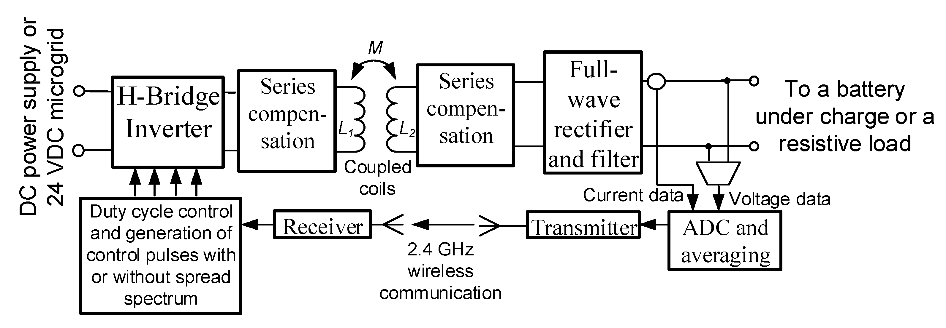
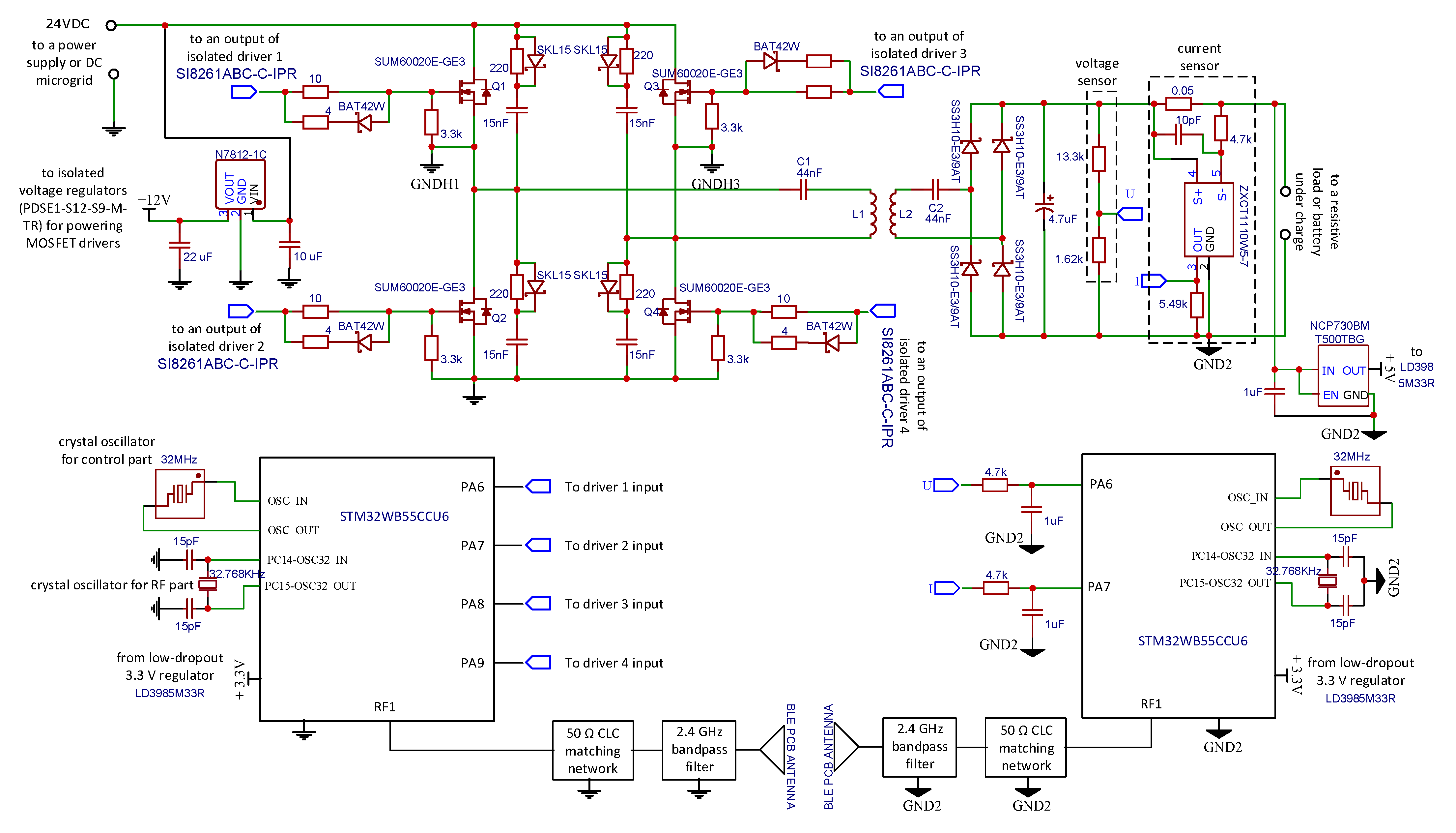
For the experimental studies, a scaled-down 50 W laboratory prototype of a wireless battery charger was designed and physically built. The prototype together with the measurement equipment is demonstrated in Figure 2. A block diagram and simplified schematic diagram of the designed wireless battery charger are depicted in Figure 3 and Figure 4, respectively.
The designed wireless battery charger primary side has an H-bridge inverter (with four surface-mount transistors having low-drain-to-source resistance), four RCD snubber circuits, four isolated MOSFET drivers (with some auxiliary external components), two polymer film capacitors connected in parallel (with low equivalent series resistance) for the series compensation, four isolated step-down switch-mode power converters (with same external components) for powering the drivers, one switch-mode step-down converter to convert input voltage 24 V to output voltage 12 V, a relatively inexpensive microcontroller (with internal transceiver circuit) STM32WB55CCU6, with some external components (e.g., crystal oscillators), the transmitting coil L1 and PCB antenna (Figure 4). The secondary side of the charger is more compact, and it has the receiving coil L2, two polymer film capacitors connected in parallel (for the series compensation), full-wave rectifier with Schottky diodes followed by the filtering capacitor, as well as current and voltage sensors. The control part of the secondary side is represented by the same microcontroller (with some external components) as in the primary side and PCB antenna. The secondary-side microcontroller is necessary to: (1) gather data from the output sensors every 10 ms; (2) make analog to digital conversion; (3) average a set of ten measurement results; (4) prepare data for the transmission; (5) generate a modulated 2.4 GHz signal for Bluetooth low energy (BLE) communications. The primary side microcontroller receives the data due to the wireless communication link between it and the secondary-side microcontroller, and then, the primary-side microcontroller completes the following actions: it computes the duty cycle of the MOSFETs control signals (by using digital PID controller), and it generates four square pulses with definite duty cycles to control the MOSFETs and to regulate the charger output voltage or current. In addition, the primary side microcontroller is necessary to toggle from COC to COV mode (if the output voltage is equal to cut-off charge voltage 25.2 V), to switch-off the charging process if the output current < 200 mA and to implement the multi-switching frequency technique with different parameters. A suitable code is recorded to a memory of the microcontrollers to implement COC or COV modes and the multi-switching-frequency schemes.
The wireless charger specifications are presented in Table 1. It can be applied to small mobile robots for 6-cell Li-ion or Li-polymer battery charging under COC mode followed by COV mode. The designed prototype can allow us to study the effect of different parameters of the multi-switching-frequency technique on the performance characteristics of the wireless battery charger and to compare the results to the performance characteristics of the conventional wireless charger without the spread-spectrum techniques.
The operating frequencies for the multi-switching frequency technique can be chosen within the Qi-standard-allowed range of frequencies. As DC input voltage, the voltage of 24 V is chosen, because of the high popularity of 24 V DC microgrids. The resonant frequency (frez) of the primary resonant tank was approximately 150 kHz. The switching frequency of the charger without the spread spectrum or the second frequency f2 of the charger with the three-switching frequency scheme was equal to frez approximately. Since the input equivalent resistance of a battery under charge increases from 11.1 to 126 Ω, instead of the battery, we used an electronic load LD300 in constant resistance mode. The range of the load resistances 11.1–12.6 Ω corresponds to COC, but the range of the resistances 12.6–126 Ω corresponds to COV. The boundary resistance between COC and COV is 12.6 Ω.
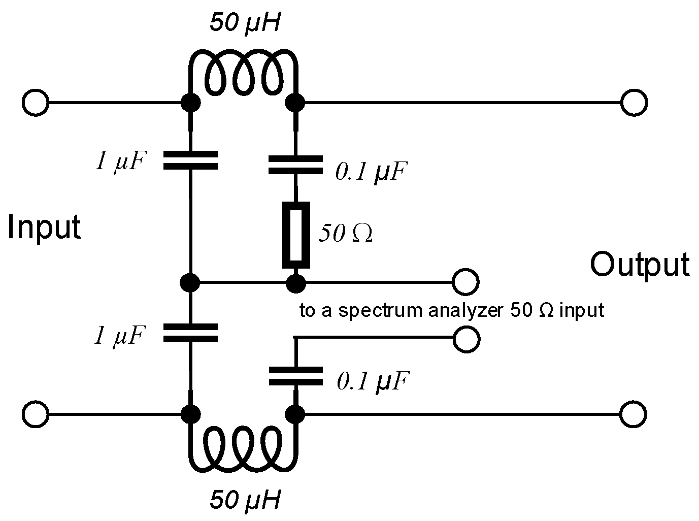
In the conducted emissions measurements, we used home-made LISN (Figure 2), the schematic diagram (Figure 5) of which corresponds to a simplified version of a factory-made LISN with CISPR specifications. During the efficiency (η) measurements, LISN was disconnected from the circuit. The conducted emissions spectrum (at the high-frequency output of LISN) was analyzed in the frequency domain according to the requirements of the international standard CISPR11: the measurement frequency range 0.15 MHz –30 MHz; resolution bandwidth (RBW) 9 kHz. For the conducted emissions measurements, a mixed domain oscilloscope Tektronix MDO4034B with a built-in spectrum analyzer (with a peak detector) was used. For the primary coil current measurements, a wide-bandwidth current probe Tektronix was used.

3.2. Design of the Experimental Prototype

In this subsection, it will be shown how the main circuit components were chosen. In the calculations, it is assumed that there are no losses in the circuit; the resonant tank currents are sine, and maximum RMS values of currents of the power components are at the boundary between COC and COV modes (load resistance Rload = 12.6 Ω).
Initially, we should know the values of inductances of the receiving and transmitting coils (L1 and L2, respectively). We used Ansys Maxwell computational electromagnetics software to model the coils at different distances and misalignments. The following assumptions were made during the modeling: the ferrite pad is KEMET FPL100 (100 × 100 × 4 mm; relative magnetic permeability 3000 and saturation field 520 mT); the coils outer diameter is 84 mm; the coils inner diameter is 55 mm; there is only single layer of copper wire. The modeling results showed: the inductances of the coils are 27 µH at the rated distance of 2.8 cm (the coils are aligned perfectly); the mutual inductance M between the coils is 9 µH at the rated distance between the coils (the coils are aligned perfectly); M = 8.25 µH (with the maximum misalignment of 1 cm).
In order to choose litz wire for the transmitting coil, the RMS value of the coil current must be calculated using the following expression [17]:
I L 1 r m s = V 1 r m s Z r e f
where Z r e f is the referred impedance from the secondary side to the primary side of the WPT system, Z r e f = ω 2 M 2 R e q [17]; R e q is the equivalent load resistance, R e q = 8 π 2 R l o a d [18] ( R l o a d is the load resistance); V 1 r m s is the inverter output voltage fundamental harmonic RMS value, V 1 r m s = 2 2 ω M V o u t π R e q [18].
Assuming that the maximum RMS value of the transmitting coil current is at the worst-coupling case (M = 8.25 µH) and when Rload corresponds to the boundary between COC and COV modes (Rload in this case equals 12.6 Ω), we calculated using (1) that I L 1 r m s = 2.92 A; R e q = 10.22 Ω; Z r e f = 5.9 Ω; V 1 r m s = 17.21 V. Considering that I L 1 r m s = 2.92 A, we choose litz wire CLI 200/120 (120 strands; effective cross section area of 0.943 mm2), which can sustain AC currents with RMS values up to 3.36 A. Note that the calculations are made assuming that the charger operates at a single frequency f = 150 kHz, and if the charger operates at three different frequencies, RMS value of the current may increase. However, as is shown in simulations of the charger in the PSIM software, the increase in the RMS value is relatively low (few% only) and, therefore, litz wire CLI 200/120 can be used even if there is a spread spectrum. After calculating peak magnetic field density in the coil L1 ferrite pad (for the worst-case coupling), it was concluded that it is well below the saturation field of the ferrite pad KEMET FPL100. Simulations of the charger circuit in the PSIM software showed that the multi-switching-frequency scheme can increase the peak value of the coil L1 current by up to 30%, but the selected ferrite will not be saturated because of its relatively large saturation field.
In order to choose a litz wire for the receiving coil, the RMS value of the coil current must be calculated using the following expression [18]:
I L 2 r m s = π 2 I o u t 4
where I o u t is the charger output DC current. Assuming that the maximum value of I o u t = 2 A is in COC mode, it can be calculated that I L 2 r m s = 2.21 A. Thus, as a litz wire and ferrite pad, we can use CLI 200/120 and KEMET FPL100, respectively.
Capacitances of the compensation capacitors C1 and C2 can be calculated using the well-known Thomson formula as follows:
C 1 = 1 4 π 2 f 2 L 1   =   41.74   nF ,
C 2 = 1 4 π 2 f 2 L 2   =   41.74   nF .
In order to choose correct capacitors, we should know peak voltage across them and the current RMS value. It is obvious that the total current RMS value through C1 is I L 1 r m s = 2.92 A, but the total current RMS value through C2 is I L 2 r m s = 2.21 A. Taking into account that a waveform of the currents through the capacitors is sine, peak voltages across the capacitors may be calculated using the following expressions:
V C 1 p e a k = 2 I L 1 r m s ω C 1
V C 2 p e a k = 2 I L 2 r m s ω C 2
Calculating for the worst-case coupling, we can obtain from (5) and (6) that V C 1 p e a k = 104.7 V and V C 2 p e a k = 79.24 V. Thus, (5) and (6) are valid only for operation at single-switching frequency. If a multi-switching-frequency scheme is used, then peak values of the voltages may increase. As the simulations in PSIM show, the peak values increase up to 30%. This will be taken into account when choosing the capacitors. Therefore, for C1 (and C2), we used two 22 nF ± 10% polymer film capacitors connected in parallel. Each capacitor has a current rating of 2 A and maximum allowable voltage of 200 V.
In order to choose correct rectifying diodes of the diode bridge at the receiving side, we should know each diode reverse voltage peak value (VDrev) and forward average current (Ifavg) at the worst case coupling and maximum output DC voltage in COC mode (Rload = 12.6 Ω). It is obvious that VDrev for each rectifying diode is equal to the output DC voltage 25.2 V approximately, but Ifavg is two times lower than output DC current (2 A) in COC mode. Thus, for the diode bridge at the receiving side, we used SS3H10-E3/9AT Schotky diodes with maximum allowable forward average current of 3 A and maximum allowable peak reverse voltage of 100 V.
In order to choose correct H-bridge transistors (Q1–Q4) at the transmitting side, we should know each transistor drain-to-source voltage peak value (Vds) and drain current RMS value (ITrms) at the worst-case coupling and maximum output DC voltage in COC mode (Rload = 12.6 Ω). Assuming that the parasitic spike voltage (Vspike) between the drain and source terminals of each transistor will be equal to the input voltage, total Vds will be Vin + Vspike = 48 V. The snubber circuits (see Figure 4) should be designed to limit the spike voltage to 24 V. The maximum value of the drain current, if Q1 and Q4 are on during one half a period, and Q2 and Q3 are one on within another half a period, will be:
I T r m s m a x = 2 V i n π Z r e f   =   2.59   A .
Thus, for the H-bridge inverter, we used four SUM60020E low-on-resistance Si MOSFETs with maximum allowable drain-to-source voltage of 80 V and sufficient maximum allowable drain current RMS value. After making thermal calculations, we concluded that the MOSFETs can be mounted on the copper pads with a minimum recommended pad area (in their data sheet).
The external components of the current sensor, both microcontrollers and the drivers were chosen according to recommendations presented in their data sheets [19,20].

4. Results and Discussion

The designed and fabricated wireless battery charger’s output voltage and current were measured for different values of the load resistances (11.1 Ω–126 Ω). As it is seen in Figure 6, the charger performs well because COC and COV modes are achieved: the charging current is almost constant (approximately 2 A) in COC mode, and the charging voltage is also almost constant (approximately 25.2 V) in COV mode. When the load resistance equals 12.6 Ω, then the charger toggles from COC mode to COV mode. The charging profiles are similar for the charger without the multi-switching frequency scheme or with it.
The primary side microcontroller generates the control signals (Figure 7) of the H-bridge inverter MOSFETs to control the charger output voltage or current through the duty cycle variation. As the load resistance increases, the duty cycle of the MOSFET Q1 decreases, and it results in a decrease in the pulse width of the inverter output voltage (Figure 8). Since the inverter switching frequency is close to the primary resonant tank resonance frequency, the waveform of the output current of the inverter is close to a sine waveform (Figure 8) regardless of the load resistance. For normal operation of the H-bridge inverter, the primary-side microcontroller also introduces some switching dead times to prevent Q1 and Q2 or Q3 and Q4 from being on simultaneously (Figure 7).
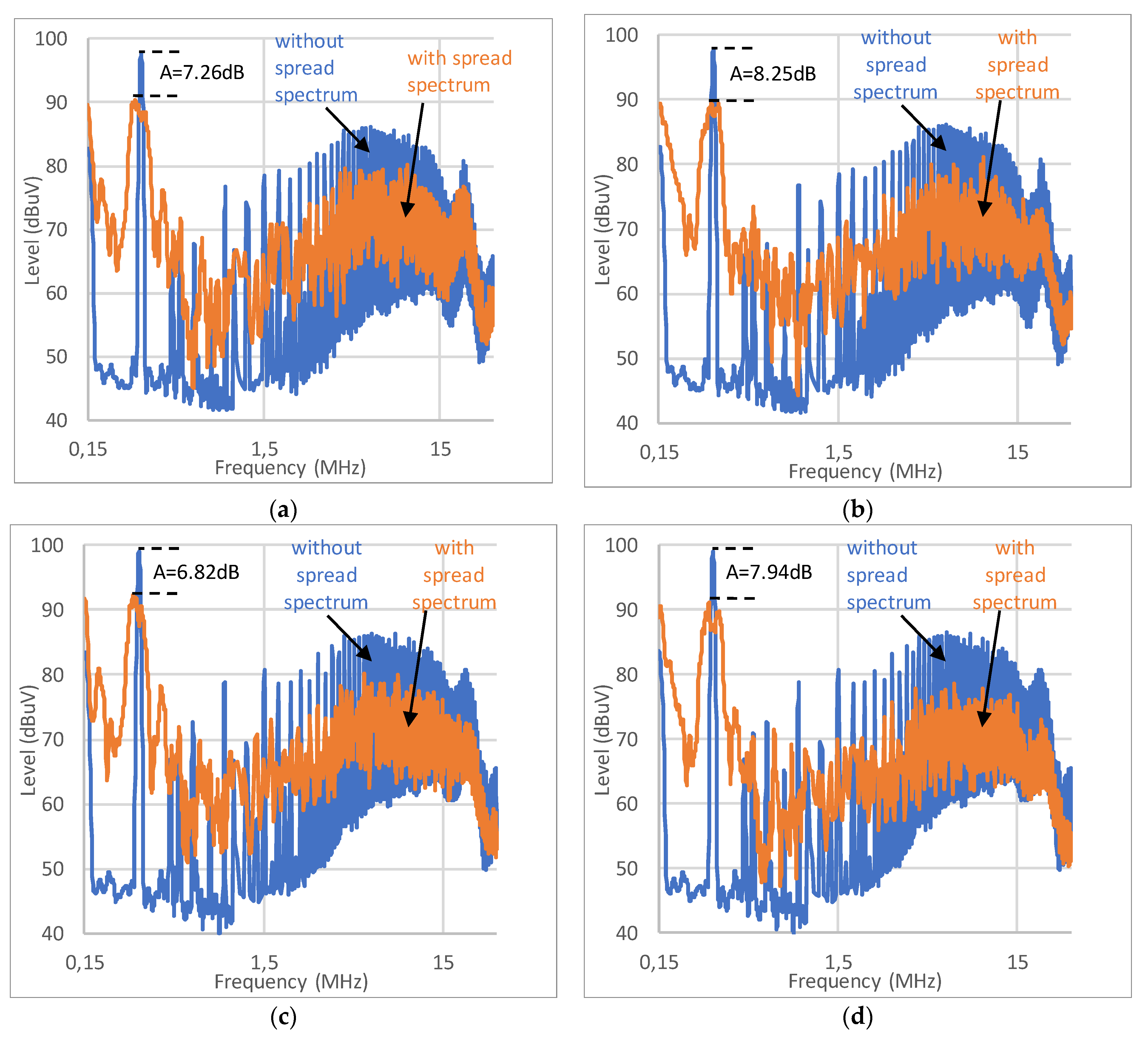
The main comparison of the performance characteristics of the wireless battery charger without the multi-switching frequency technique with that of the wireless charger with the multi-switching frequency technique (for different cases) is presented in Table 2, Table 3, Table 4 and Table 5. Additionally, a comparison of the conducted emissions spectra of conventional charger (without the spread spectrum) and the charger with the multi-switching frequency technique is presented for different cases in Figure 10. Attention should be paid to the results presented in Table 4, because if the load resistance is 18 Ω and the lateral misalignment is the maximum (1 cm), then the maximum conducted emission level is the highest. The reduction coefficient (A) of the conducted emissions is calculated as the difference (expressed in dB) between maximum level of the emissions for the charger without the spread spectrum and the charger with the spread spectrum (with the multi-switching frequency technique) within the frequency range 0.15–30 MHz (see Figure 10).
During the experiments, it was found that the conducted emission levels, the efficiency, the transmitting coil current RMS value (Irms) and the peak value (Ipeak) depend on the parameters of the multi-switching frequency scheme (see Table 2, Table 3, Table 4 and Table 5). The measurement results are shown in the tables when the modulation frequency is approximately 10 kHz, when the three-switching-frequency spread spectrum technique is used and when the difference between the adjacent frequencies (f2-f1) is 15 kHz. The selection of those parameters led to the best results in terms of the reduction of the conducted emissions and the efficiency.
As it is seen from Table 2, Table 3, Table 4 and Table 5, an optimum combination of the number of pulses and the order of frequencies exists for the highest reduction coefficient (A) of the conducted emissions for a given load resistance and the misalignment. For example, if the load resistance is 18 Ω and the lateral misalignment is the maximum, the optimum combination of the number of pulses is 4, 7, 4 when f3 > f2 > f1, but if the load resistance is 18 Ω and the coils are aligned perfectly, then the optimum combination of the number of pulses is 5, 4, 6 when f3 < f2 < f1. Therefore, for the best performance, the primary-side microcontroller should choose the optimum parameters depending on the different misalignments and the load resistances. However, it would lead to an increased usage of the microcontroller memory and the computational resources. Therefore, in many cases, we think that it is enough to find an optimum combination only for the worst-case scenario (in terms of the highest emission levels), which in our case, is with the load resistance of 18 Ω and the maximum lateral misalignment of the coils. The optimum combination of the number of pulses and the frequency order were determined experimentally using the trial and error approach.
The obtained results also show that the multi-switching frequency technique compared to the conventional control (without the spread spectrum) leads to a significant reduction of the conducted emissions (up to 8.5 dB, if optimum parameters are used) with slight decreases in the efficiency (<0.3% in COC mode) or with an improvement in the efficiency (up to 0.7% in COV mode). The experiments also showed that at higher load resistances (>40 Ω), the proposed optimum multi-switching frequency technique gives even better improvement of the efficiency (up to 1.5%) when compared to the control technique without the spread spectrum. However, the peak and RMS values of the coils (and other power components) may increase with use of the multi-switching frequency technique. However, the increase in RMS values is low (only few%), but increases in the peak values are moderate (<30%), which is also seen in Figure 9. Such an increase in the peak values of current is not a problem for the power diodes, transistors and compensation capacitors, but it can be a problem for the coils with ferrite pads, because the ferrite can be saturated if the peak value of current through the coil exceeds the saturation limit. Therefore, the ferrite pads with moderately higher saturation current should be chosen for the wireless battery chargers with the multi-switching frequency technique.
The presented results (Table 2, Table 3, Table 4 and Table 5 and Figure 10) also show that the multi-switching frequency technique with the optimum combination of number of pulses and the optimum order of the frequencies gives noticeably better reduction of the conducted emissions than that of the classical multi-switching-frequency technique (N1 = N2 = N3, f3 > f2 > f1) for different load resistances and the misalignments. However, the efficiency and the peak and RMS values of the coil current are similar when the optimum and classical multi-frequency techniques are used.
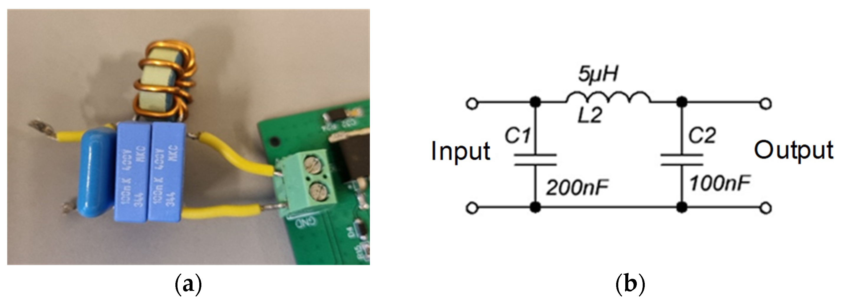
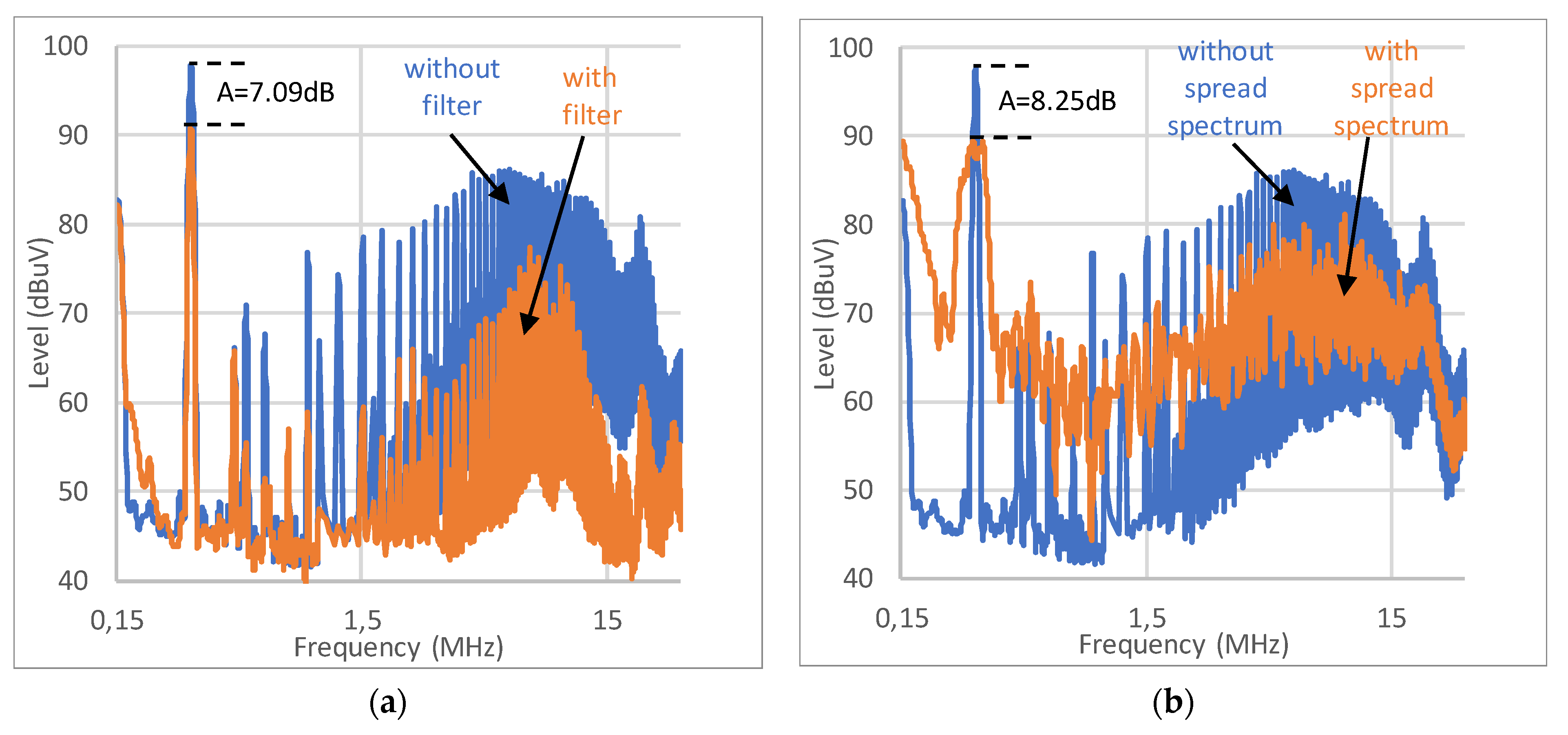
In order to estimate the level of the reduction of the volume of the wireless charger primary side, a conducted emissions filter (Figure 11) was developed with the coefficient of the reduction of the conducted emissions (A) similar to that of the optimum three-switching frequency technique. The filter volume was about 10% of the total volume of the primary side of the charger. The main results are presented in Figure 12 and Table 6 for a comparison of the performances of the wireless charger with different cases (without the filter and the spread spectrum; with the filter but without the spread spectrum and without the filter but with the multi-switching-frequency technique). We concluded that the volume of the primary side of the wireless battery charger can be reduced noticeably (by at least 10%), with slightly better efficiency and reduced cost of the charger, if the proposed optimum multi-frequency technique is used.

5. Conclusions

The original thorough experimental study of the effect of the multi-switching-frequency-based spread spectrum technique parameters on the performance characteristics of the inductive-resonant wireless battery charger with a closed-loop control showed that the combinations of the number of pulses and the frequency order have a noticeable impact on the conducted emissions levels, efficiency peak and RMS values of the coil current of the wireless charger. The suppression of the conducted emissions can be improved significantly using the optimum parameters of the technique. The presented results also show that the multi-switching frequency technique with the optimum combination of number of pulses and the optimum order of the frequencies gives noticeably better reduction of the conducted emissions than that of the classical multi-switching-frequency technique (N1 = N2 = N3, f3 > f2 > f1) for different load resistances and the misalignments, but the efficiency, the peak and RMS values of the coil current are similar when the optimum and classical multi-frequency techniques are used. The proposed optimized technique only slightly reduces the efficiency of the conventional wireless charger (without the spread spectrum) in COC mode (<0.3%), but it can increase the efficiency by up to 1% in COV mode (at higher load resistances).
Moreover, it is proved experimentally that a relatively inexpensive microcontroller with a transceiver can be used to implement both closed-loop control of the wireless charger and the multi-switching-frequency technique. The volume of the primary side of the wireless battery charger can be reduced noticeably (by at least 10%), with slightly better efficiency and reduced cost of the charger if the proposed optimum multi-frequency technique is used. The only concern with the use of the multi-frequency technique is that the coils’ currents can increase moderately (<30%); therefore, when choosing ferrite pads for the coils of the wireless battery charger with the multi-switching frequency technique, this point must be taken into account to prevent the ferrite from saturation.

Author Contributions

Conceptualization, D.S.; methodology, D.S. and A.S.; software and design, A.S.; validation, A.S. and D.S.; formal analysis, D.S. and A.S.; data curation, A.S.; writing—original draft preparation, D.S.; writing—review and editing, J.Z.; visualization, A.S.; supervision, J.Z.; project administration, J.Z. All authors have read and agreed to the published version of the manuscript.

Funding

This work has been supported by the European Regional Development Fund within the Activity 1.1.1.2 “Post-doctoral Research Aid” of the Specific Aid Objective 1.1.1 “To increase the research and innovative capacity of scientific institutions of Latvia and the ability to attract external financing, investing in human resources and infrastructure” of the Operational Programme “Growth and Employment” (No.1.1.1.2/VIAA/3/19/415).

Data Availability Statement

Data of our study are available upon request.

Acknowledgments

We would like to express our gratitude to A. Zhiravecka for her help in improving English grammar.

Conflicts of Interest

The authors declare no conflict of interest.

References

  1. Liao, J.H.; Lin, Y. A Novel Bidirectional Wireless Power Transfer System for Mobile Power Application. Appl. Sci. 2019, 9, 3769. [Google Scholar] [CrossRef] [Green Version]
  2. Hou, J.; Cao, Y.; Zeng, H.; Hei, T.; Liu, G.X.; Tian, H.M. High efficiency wireless charging system design for mobile robots. IOP Conf. Ser. Earth Environ. Sci. 2018, 188, 012032. [Google Scholar] [CrossRef]
  3. Mulders, J.; Delabie, D.; Lecluyse, C.; Buyle, C.; Callebaut, G.; Perre, L.; Strycker, L. Wireless Power Transfer: Systems, Circuits, Standards, and Use Cases. Sensors 2022, 22, 5573. [Google Scholar] [CrossRef] [PubMed]
  4. Li, Y.; Duan, Q.; Zou, Y. High Robustness Control for Robotic Wireless Power Transfer Systems with Multiple Uncertain Parameters Using a Virtual Buck Converter. Energies 2017, 10, 517. [Google Scholar] [CrossRef] [Green Version]
  5. Stepins, D.; Zakis, J.; Audze, J.; Husev, O.; Pakhaliuk, B. Comparative Analysis of Different Spread-Spectrum Techniques for Reduction of Conducted Emissions Generated by Magnetic Resonant Wireless Power Transfer Systems. In Proceedings of the IEEE 2nd Ukraine Conference on Electrical and Computer Engineering (UKRCON), Lviv, Ukraine, 2–6 July 2019; pp. 448–454. [Google Scholar]
  6. Simonazzi, M.; Sandrolini, L. Conducted Emission Analysis of a Near-Field Wireless Power Transfer System. In Proceedings of the IEEE 15th International Conference on Compatibility, Power Electronics and Power Engineering (CPE-POWERENG), Florence, Italy, 14–16 July 2021; pp. 1–6. [Google Scholar]
  7. Zimmer, S.; Helwig, M.; Winkler, A.; Modler, N. Modeling Electrical Conductivity of Metal Meshes for Predicting Shielding Effectiveness in Magnetic Fields of Wireless Power Transfer Systems. Electronics 2022, 11, 2156. [Google Scholar] [CrossRef]
  8. Ferber, M.; Mrad, R.; Morel, F.; Pillonnet, G.; Vollaire, C. Power Efficiency and EMI Attenuation Optimization in Filter Design. IEEE Trans. Elect. Comp. 2018, 60, 1811–1818. [Google Scholar] [CrossRef] [Green Version]
  9. Chung, S.; Kang, B. Considerations for Gain Selection of Feedforward Active EMI Filters. Symmetry 2022, 14, 1826. [Google Scholar] [CrossRef]
  10. Zhang, Y.F.; Yang, L.; Lee, C.Q. EMI reduction in power supplies by Bi-Frequency modulation. In Proceedings of the 1994 Applied Power Electronics Conference and Exposition (APEC), Orlando, FL, USA, 13–17 February 1994; pp. 601–607. [Google Scholar]
  11. Stepins, D.; Kathari, N.; Zakis, J.; Husev, O.; Pakhaliuk, B.; Shevchenko, V. Effect of Hybrid Modulation on Performance of Wireless Battery Charger Operating in CC/CV Mode. In Proceedings of the 47th Annual Conference of the IEEE Industrial Electronics Society, Toronto, ON, Canada, 13–16 October 2021; pp. 1–6. [Google Scholar]
  12. Stepins, D.; Akunuri, L.; Subbarao, A.; Zakis, J. Reduction of Electromagnetic Emissions Generated by Inductive Resonant WPT Systems Using Multi-Switching-Frequency-Based Method. In Proceedings of the IEEE 61st International Scientific Conference on Power and Electrical Engineering of Riga Technical University (RTUCON), Riga, Latvia, 5–7 November 2020; pp. 1–8. [Google Scholar]
  13. Inoue, K.; Kusaka, K.; Itoh, J. Reduction in Radiation Noise Level for Inductive Power Transfer Systems using Spread Spectrum Techniques. IEEE Trans. Power Electr. 2018, 33, 3076–3085. [Google Scholar] [CrossRef]
  14. Suzuki, M. Conducted Emission in an 85 kHz, 50 kW WPT System with Opposite-Phase Transfer and Spread Spectrum. In Proceedings of the 2019 IEEE PELS Workshop on Emerging Technologies: Wireless Power Transfer (WoW), London, UK, 18–21 June 2019; pp. 1–4. [Google Scholar]
  15. Stepins, D.; Shah, D.D.; Sokolovs, A.; Zakis, J. An Improved Spread-Spectrum Technique for Reduction of Electromagnetic Emissions of Wireless Power Transfer Systems. Electronics 2022, 11, 2733. [Google Scholar] [CrossRef]
  16. Kim, M.; Park, H.P.; Jung, J.H. Wireless Power Transfer System with Reduced EMI Emission Employing Spread Spectrum Technique. In Proceedings of the 2020 IEEE PELS Workshop on Emerging Technologies: Wireless Power Transfer (WoW), Seoul, Republic of Korea, 15–19 November 2020; pp. 370–373. [Google Scholar] [CrossRef]
  17. Dai, X.; Li, X.; Li, Y.; Hu, A.P. Maximum Efficiency Tracking for Wireless Power Transfer Systems with Dynamic Coupling Coefficient Estimation. IEEE Trans. Power Electr. 2018, 33, 5005–5015. [Google Scholar] [CrossRef]
  18. Mai, R.; Chen, Y.; Li, Y.; Zhang, Y.; Cao, G.; He, Z. Inductive Power Transfer for Massive Electric Bicycles Charging Based on Hybrid Topology Switching with a Single Inverter. IEEE Trans. Power Electr. 2017, 32, 5897–5906. [Google Scholar] [CrossRef]
  19. Microcontroller STM32WB55xx Datasheet. Available online: https://www.st.com/resource/en/datasheet/stm32wb55cc.pdf (accessed on 12 January 2023).
  20. Low Power High-Side Current Monitors ZXCT1107/1109/1110 Datasheet. Available online: https://www.diodes.com/assets/Datasheets/ZXCT1107_10.pdf (accessed on 12 January 2023).
Figure 1. Waveform of a square signal with classical 3-switching frequency technique. In this figure, N1 = N2 = N3; τ1τ2τ3; frequency order is from low to high.
Electronics 12 00687 g001
Figure 2. An image of the experimental prototype connected to the measuring equipment.
Electronics 12 00687 g002
Figure 3. A block diagram of the designed prototype.
Electronics 12 00687 g003
Figure 4. A simplified schematic diagram of the experimental prototype.
Electronics 12 00687 g004
Figure 5. A schematic diagram of the home-made LISN used in the experiments.
Electronics 12 00687 g005
Figure 6. The charging current and voltage profiles (obtained from the measurements).
Electronics 12 00687 g006
Figure 7. Waveforms of the control signals of MOSFET Q1 (blue), MOSFET Q2 (red), MOSFET Q3 (green) and MOSFET Q4 (bottom) when the load resistance is 40 Ω and without the spread spectrum. Scale: 4 µs/div; 5 V/div.
Electronics 12 00687 g007
Figure 8. The output voltage (red) and current (blue) waveforms of the H-bridge inverter: (a) the load resistance is 20 Ω; (b) the load resistance is 40 Ω. In both cases, the spread spectrum is not used. Scale: 2 A/div; 20 V/div; 2 µs/div.
Electronics 12 00687 g008
Figure 9. The waveforms of H-bridge inverter output voltage (red) and current (blue): (a) for the wireless charger without the spread spectrum (f1 = 153 kHz, load resistance 12.6 Ω); (b) for the wireless charger with the three-switching-frequency technique (f1 = 173 kHz, f2 = 153 kHz, f3 = 133 kHz; N1 = 6, N2 = 4, N3 = 5; load resistance 12.6 Ω). Scale: 2 A/div; 20 V/div.
Electronics 12 00687 g009
Figure 10. Comparison of the spectra of the conducted emissions of the wireless charger: (a) for the classical multi-switching-frequency technique (N1 = N2 = N3 = 5; f3 = 135 kHz f2 = 150 kHz; f3 = 165 kHz) without the spread spectrum (the coils are aligned perfectly); (b) for the optimum multi-switching-frequency technique (N1 = 5; N2 = 4; N3 = 6; f3 = 165 kHz; f2 = 150 kHz; f3 = 135 kHz) without the spread spectrum (the coils are aligned perfectly); (c) for the classical multi-switching-frequency technique (N1 = N2 = N3 = 5; f3 = 135 kHz; f2 = 150 kHz; f3 = 165 kHz) without the spread spectrum (the misalignment is 1 cm); (d) for the optimum multi-switching-frequency technique (N1 = 4; N2 = 7; N3 = 4; f3 = 135 kHz; f2 = 150 kHz; f3 = 165 kHz) without the spread spectrum (the misalignment is 1 cm). For all the results, the load resistance is 18 Ω.
Electronics 12 00687 g010
Figure 11. An image of the ∏ filter (a) and its schematic diagram (b).
Electronics 12 00687 g011
Figure 12. Comparison of the spectra of the conducted emissions when the filter is not used with the conducted emissions when the filter is used, (a) and the conducted emissions when the filter is not used with the conducted emissions for the case of the multi-switching-frequency technique (b). The load resistance is 18 Ω, and the coils are aligned perfectly.
Electronics 12 00687 g012
Table 1. The parameters values of the designed wireless battery charger.
ParameterNumerical ValueUnit of Measurement
Rated output current in COC mode2A
Rated output voltage in COV mode25.2V
The minimum charging current0.2A
Cut-off discharge voltage22.2V
DC input voltage24V
Range of allowed switching frequencies100 … 200kHz
L1 and L2 (at the rated distance one from another)27μH
Ferrite pad size10 × 10cm
Rated distance between the coils2.8cm
Primary and secondary compensation capacitance nominal values44nF
The coupling coefficient (when the coils aligned perfectly)0.33-
Maximum lateral misalignment of the coils1cm
Table 2. The performance characteristics of the wireless battery charger without the multi-switching-frequency technique and with the technique (with different combinations of a number of pulses and the order of the switching frequencies). The load resistance is 18 Ω, and the coils were aligned perfectly.
Type of Multi-Freq. Tech.f1, f2, f3 (kHz)N1, N2, N3η (%)Max Level of Emissions (dBμV)A (dB)Ipeak (A)Irms (A)fm (kHz)
without multi-freq. tech.153-78.8197.7-3.752.64-
Classical 138, 153, 1685, 5, 578.9890.47.264.302.7010.13
Modified multi-freq. tech.6, 4, 579.1791.06.744.742.7410.06
4, 7, 479.4090.27.534.502.6810.15
Classical168, 153, 1385, 5, 578.9489.87.864.302.7110.13
Modified multi-freq. tech.6, 4, 578.8190.37.414.282.6810.19
4, 4, 779.0691.06.675.122.749.93
Optimum5, 4, 678.9289.48.254.662.7210.06
Table 3. The performance characteristics of the wireless battery charger without the multi-switching-frequency technique and with the technique (with different combinations of a number of pulses and the order of the switching frequencies). The load resistance is 12.6 Ω and the coils were aligned perfectly.
Type of Multi-Freq. Tech.f1, f2, f3 (kHz)N1, N2, N3η (%)Max Level of Emissions (dBμV)A (dB)Ipeak (A)Irms (A)fm (kHz)
without multi-freq. tech.153-83.0094.4-3.812.68-
Classical138, 153, 1685, 5, 582.6590.83.604.552.8410.13
Modified multi-freq.6, 4, 582.7890.34.074.562.8410.06
4, 7, 482.7089.84.624.612.8310.15
Classical168, 153, 1385, 5, 582.4390.24.204.642.8410.13
Optimum6, 4, 582.7888.16.234.712.8010.19
Modified multi-freq.4, 4, 781.9490.83.534.812.819.93
5, 4, 681.8190.04.374.802.8510.06
Table 4. The performance characteristics of the wireless battery charger without the multi-switching-frequency technique and with the technique (with different combinations of a number of pulses and the order of the switching frequencies). The load resistance is 18 Ω, and the lateral misalignment is 1 cm.
Type of Multi-Freq. Tech.f1, f2, f3 (kHz)N1, N2, N3η (%)Max Level of Emissions (dBμV)A (dB)Ipeak (A)Irms (A)fm (kHz)
without multi-freq. tech.153-77.0399.0-4.463.11-
Classical 138, 153, 1685, 5, 576.9692.26.826.083.2010.13
Modified multi-freq. tech.6, 4, 477.2093.65.426.243.2210.7
6, 4, 576.8792.66.456.23.2110.06
Optimum multi-freq. tech. 4, 7, 477.7091.17.945.793.1610.15
Classical168, 153, 1385, 5, 576.9098.56.545.483.1710.13
Modified multi-freq. tech.6, 4, 577.0392.86.205.633.1310.19
4, 4, 777.4091.57.545.573.179.93
Table 5. The performance characteristics of the wireless battery charger without the multi-switching-frequency technique and with the technique (with different combinations of a number of pulses and the order of the switching frequencies). The load resistance is 12.6 Ω, and the lateral misalignment is 1 cm.
Type of Multi-Freq. Tech.f1, f2, f3 (kHz)N1, N2, N3η (%)Max Level of Emissions (dBμV)A (dB)Ipeak (A)Irms (A)fm (kHz)
without multi-freq. tech.153-81.2898.4-4.463.15-
Classical138, 153, 1685, 5, 581.0993.15.375.163.2910.13
Modified multi-freq.6, 4, 481.0693.05.395.573.3310.7
4, 7, 480.9692.06.385.183.2710.15
Classical168, 153, 1385, 5, 580.8791.56.885.453.3310.13
Optimum6, 4, 580.8990.87.585.353.2710.19
Modified multi-freq.4, 4, 780.9291.96.525.573.299.93
Table 6. Comparison of the measurement results for different cases (coils are aligned perfectly).
CaseLoad Resistance (Ω)η (%)A (dB)
Without filter and spread spectrum12.683.00-
With filter but without spread spectrum82.716.77
Without filter but with optimum multi-freq. tech.82.786.23
Without filter and spread spectrum1878.81-
With filter but without spread spectrum78.237.09
Without filter but with optimum multi-freq. tech.78.928.25
Disclaimer/Publisher’s Note: The statements, opinions and data contained in all publications are solely those of the individual author(s) and contributor(s) and not of MDPI and/or the editor(s). MDPI and/or the editor(s) disclaim responsibility for any injury to people or property resulting from any ideas, methods, instructions or products referred to in the content.