Article

Design of High-Order Resonator HTS Diplexer with Very Different FBW

1
School of Microelectronics, Northwestern Polytechnical University, Xi’an 710072, China
2
Yangtze River Delta Research Institute of NWPU, Taicang 215400, China
3
School of Information Science and Technology, Southwest Jiaotong University, Chengdu 611756, China
4
Department of Electronic Engineering, Shanghai Jiao Tong University, Shanghai 200030, China
*
Authors to whom correspondence should be addressed.
Electronics 2023, 12(3), 691; https://doi.org/10.3390/electronics12030691
Submission received: 17 December 2022 / Revised: 11 January 2023 / Accepted: 17 January 2023 / Published: 30 January 2023
(This article belongs to the Section Circuit and Signal Processing)

Abstract

:
Adopting the deformed stepped impedance micro-strip line structure resonators (SIRs), the external weak coupling hairpin SIR (HSIR) and external strong coupling opening SIR (OSIR) resonators are designed, respectively. These two types of resonators are convenient for creating an ultra-narrow band and broadband filters, respectively, and can broaden the second harmonic passband. A high isolation diplexer without an impedance matching structure is realized by cascading 12-order and 14-order HTS filters composed of OSIR and HSIR resonators with a high isolation T-shaped structure. The diplexer is fabricated on a thin YBCO/MgO/YBCO (a MgO wafer with YBa2Cu3O7 thin film deposited on both sides) film with a dimension of 31.85 mm × 17.28 mm, a thickness of 0.5 mm, and a dielectric constant of 9.8. At 77 K, the measured central frequency of the diplexer is 2395 MHz and 3300 MHz, the fractional bandwidths (FBW) are 1.25% and 24.24%, the out-of-band rejections are greater than 60 dB/MHz, the 2f0 are located at 5.1 GHz and 6.6 GHz, the insertion loss is less than 0.20 dB, and the return losses are better than 16 dB and 15 dB. The diplexer has the advantages of a simple design method, compact structure, low insertion loss, high sideband rejection, and high isolation.

1. Introduction

The microwave diplexer is an essential component in frequency division duplex technology, which includes a transmission filter, reception filter, and matching network. It is a microwave device integrated with a transceiver and has various applications in microwave technology and wireless communication systems. In the differential frequency duplex communication system, the diplexer is located in the RF front-end circuit and connected with the transceiver antenna, which can ensure that the microwave system can generally transmit typically simultaneously, but also can isolate the received and transmitted signals. Therefore, the alerts can send signals of two frequencies to the transmitting and receiving channels, respectively, when they are working so that they can work independently without disturbing each other. In terms of application, necessarily, it is a vital standard to consider the performance of the diplexer to divide different frequencies without interfering with each other at the expense of the minimum loss, that is, the insertion in the band and the out-of-band suppression of the diplexer. These performances of the diplexer will also directly affect the sensitivity and anti-interference ability of the receiver. The current research shows that the cavity diplexer has a good advantage in terms of insertion loss, but the relative bandwidth is narrow, and the insertion loss is significant. For example, the insertion loss of a circular cavity dual-mode diplexer can be minimal. Still, the installation angle needs to be designed separately, and the working bandwidth is relatively narrow [1,2]. At the same time, the oversize of the cavity filter also limits its engineering application. The bulk acoustic wave and substrate-integrated waveguide diplexers that can achieve miniaturization have problems in the signing process, design complexity, and performance [3,4,5]. Micro-strip diplexers, including the GaAs and Si substrate diplexers, meet the development requirements of low cost, miniaturization, and high-frequency band in the industry. However, its disadvantages are its low-quality factor and high intern loss [6,7]. The HTS diplexer was developed based on the micro-strip diplexer to solve this contradiction. The HTS thin film materials have meager surface resistance in the microwave frequency band. Therefore, the planar filter and diplexer made of HTS film can deal with filter insertion loss and filter order [8]. Moreover, the HTS diplexer with a high-order resonator coupling structure exhibits superior comprehensive performance than the traditional microwave filter in terms of microwave loss and frequency selection characteristics [9,10,11]. In [9,10,11], HTS dual-band, three-band, and four-band filters have been designed, respectively, and the advantages of the HTS multiplexer design have been preliminarily reflected upon.
Diplexers working across different frequency ranges and bandwidths have been required with the continuous occupation of spectrum resources and the diversified development of radar and communication systems, as shown in Figure 1. Still, it is challenging to design with very different FBW in two bands. When the operating frequency and bandwidth of Channel I and Channel II differ significantly, and the 2f0 of Channel I is located near Channel II, the diplexer design has tremendous challenges in isolation and sideband suppression systems. In this paper, a compact diplexer containing an ultra-narrow band and a wide band is designed, which solves the problem that the operating frequency band and the relative bandwidth is very different between the two passbands, and realizes the high isolation between the two passbands. Finally, the sideband suppression profited from high-order resonators and the intra-passband characteristics on account of the HTS film achieving good results.

2. Synthesis of Diplexer Coupling Matrix

2.1. Synthesis of Filter Coupling Matrix

Two high-order Chebyshev filters need to be designed separately according to the Chebyshev filter synthesis technology proposed by Cameron [12], and recorded as filters A and B. Firstly, the low-pass prototype transmission functions S21(ω) and S11(ω) are calculated. Then, assuming that the normalized impedance is 1 in both the source and load, the admittance matrices YA(ω) and YB(ω), and the N + 2 order normalized coupling matrices of filters A and B are calculated, respectively. According to the index parameters of the two bandpass filters of the diplexer in Table 1, the coupling matrix and the external quality factor (Q) are calculated according to Equations (1–3) [2], as shown in Table 2, where Mi,j represents the coupling coefficient between the resonators i and j in the filter prototype, mi,j represents the coupling coefficient between the resonators i and j in the filter, BW represents the bandwidth, and FBW represents the fractional bandwidth.
Q e = g 0 g 1 F B W = 1 F B W M S 1 2 = 1 F B W M N L 2
M i , j = F B W g i g j
m i , j = M i , j B W f 0

2.2. Synthesis of Diplexer Coupling Matrix

A. Morini et al. considered the T-junction as a part of the filter, and then realized the design of the T-junction diplexer by adjusting the filter connected to the T-junction to adapt to the influence of the complex impedance brought by the T-connector [13]. G. Macchiarella et al. further synthesized the micro-strip diplexer. Their idea was to design two conventional passband filters, respectively, and then optimize the whole diplexer until the performance met the design requirements [14]. This design method is more applicable to the high-temperature superconducting diplexer. In this paper, the T-junction matching method is used to parallelize two SIR filters with different structures, so a compact diplexer containing an ultra-narrow band and a wide band is designed, which solves the problem that the operating frequency band and the relative bandwidth is very different between the two passbands, and realizes the high isolation between the two passbands.
The design of the band-pass filter is mainly to solve the problems of resonance and coupling, but the creation of the diplexer is primarily to achieve the matching; that is, it is necessary to fully consider the matching of each port and use all methods to achieve good matching. According to the characteristics of the transmission micro-strip line, a solution can be obtained to make the transmission line in an open state in the first half wavelength for a section of the transmission line with one port connected with a reactive load. Therefore, one end of the two transmission lines relates to the filter of the two channels, and the other is connected to the expected end. Then, adjusting the tail port of each transmission line to the open state for the filter connected to another transmission line can counteract the influence of the introduced admittance on the channel characteristics. The method described above is called a T-junction matching network, which is effective in the design of the HTS diplexer. The input impedance of the micro-strip T-junction shall meet the following conditions.
Z i n 1 = @ f II 50 Ω @ f I
Z i n 2 = 50 Ω @ f II @ f I
After completing the design of two A and B filters with a 50 Ω load connected at both ends, the coupling matrix of the diplexer is synthesized based on the analysis of Equation (4), where @ fx indicates that passband x (x = I or II) operates at frequency fx. At this time, the source end admittance of filter B changes from Ys to Ys + YinA, where YinA is the source input admittance of filter A, as shown in Figure 2. Since the admittance matrix YA(f) of filter A has been calculated in the previous part, the source input admittance YinA of filter A can be calculated according to Equation (5).
Y inA = Y 11 + Y 12 + 1 1 Y 11 + 1 Y 22 + Y 12 + Y L
Y A ( f 2 ) = Y 11 Y 12 Y 21 Y 22
where YL is the normalized load admittance, here it is 1. Y11, Y12, and Y22 are the elements in the admittance matrix YA (f) of filter A. The filter network is reciprocal, so Y21 = Y12, where ƒ2 is the center frequency of filter B. Next, the iterative method will be used to optimize the coupling matrix of filters A and B. The iterative process is as follows:
1
Assuming that the center frequencies of filters A and B are f1 and f2, respectively, take the initial source impedance Y1(0) = Y2(0) = YS = 50 Ω of filters A and B, with the allowable error ε a and ε b > 0. In this design, set ε a = ε b = 0.001, and k = 1.
2
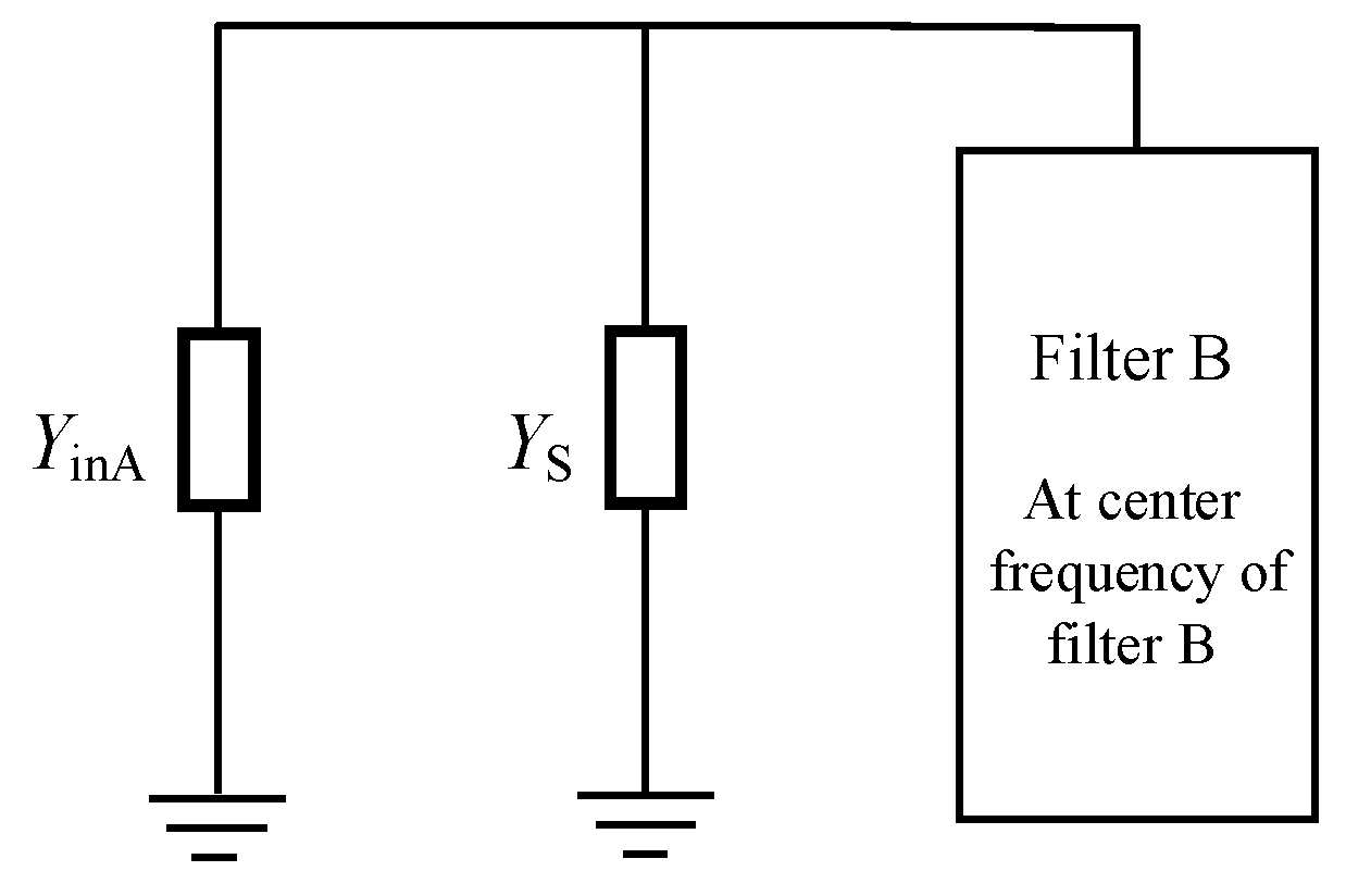
Set the source admittance of filter A as Y1 (k − 1), and recalculate the coupling matrix M1 (k) of filter A. Set the source impedance of filter B to Y2 (k − 1), and recalculate the coupling matrix M2 (k) of filter B. Stop iteration when the formula (6) is established.
Y 1 ( k ) Y 1 ( k 1 ) Y 1 ( k ) < ε a , Y 2 ( k ) Y 2 ( k 1 ) Y 2 ( k ) < ε b
3
When the source impedance is Y1 (k − 1) and the coupling matrix is M1 (k), calculate the input admittance YinA (k) of filter A at f2; then, the source impedance of filter B becomes Y2 (k) =Ys + Y1 (k). When the source impedance is Y2 (k − 1), and the coupling matrix is M2 (k), calculate the input admittance YinB(k) of filter B at f1; then, the source impedance of filter B becomes Y1 (k)= Ys + YinB (k).
4
Let k = k + 1, and return to Step 2.
The principle circuit is calculated iteratively based on the coupling coefficient of filter A and filter B by the ADS simulation software. Then, band-pass filters A and B are connected in parallel by T-junction branches corresponding to Channels I and II. The two passband filters’ coupling coefficient and external quality factor are simulated and iteratively optimized, respectively. The matching of the two passbands of the T-junction is completed to obtain acceptable performance parameters inside and outside of the two passbands. Finally, the coupling matrix coefficients of the diplexer are obtained and shown in Table 3. Due to the introduction of the T-junction, the coupling coefficients of the two filters in the diplexer are no longer about the central (m6,7) symmetric.

3. Verification of Proposed Configuration

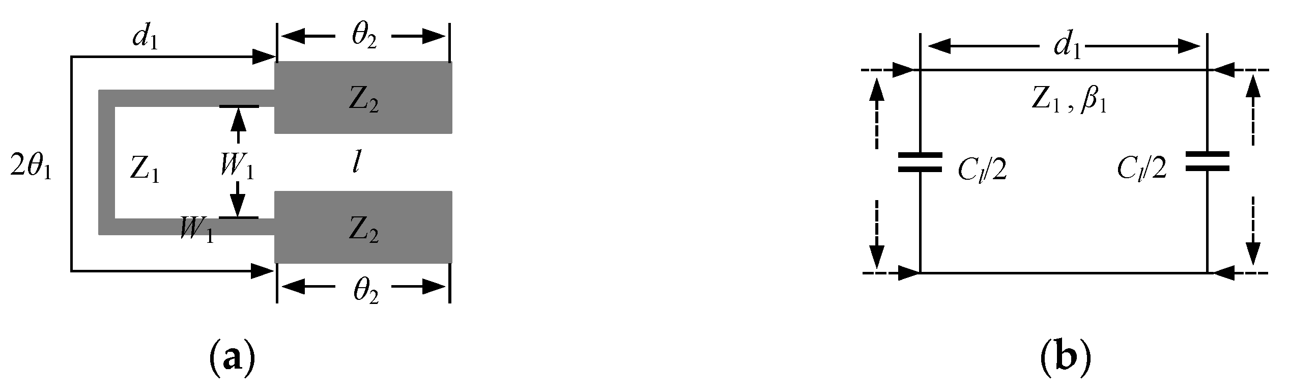
3.1. Analysis of the SIR Resonator

A stepped impedance resonator (SIR) is a typical structure used in the design of band-pass filters with a width of second harmonic; the name of its construction is proposed by the relatively uniform impedance resonator (UIR). The principle of stepped impedance is to cascade transmission lines with different characteristic impedances and change the frequency ratio of the harmonic wave to the fundamental wave by varying its impedance ratio to control the frequency of the harmonic wave and adjust the position of the second harmonic.
For the SIR resonator in Figure 3, Cl is the loaded capacitance of low impedance, and Z1, β1, and d are the characteristic impedance, the propagation constant, and the length of the unloaded line, respectively. The electric length 2 θ = β 1 d i (i = 1/2), so θ1 and θ2 represent the electrical lengths of the base mode and the second parasitic mode, respectively, and can be expressed by Equations (7a) and (7b).
θ 1 = 2 tan 1 1 π f 1 Z l C L
The fundamental resonant frequency f1 and the second spurious resonant frequency f2 can be determined. Now, it can be seen from Equations (7a) and (7b) that θ 1 = π and θ 2 = 2 π when Cl = 0. This is the case for the unloaded half-wavelength resonator. When Cl ≠ 0, the resonant frequencies are shifted down as the loading capacitance increases, indicating a slow-wave effect.
When Cl takes different values, the SIR corresponds to different values, and the impedance ratio is defined as:
K = Z 2 Z 1
if the length ratio of the SIR is defined as:
α = θ 2 θ 2 + θ 1
It should be noted that the fundamental frequency and the other higher order mode frequencies can be determined by properly choosing a suitable combination of the impedance and the length ratios of the SIR.
The ratios of the second spurious frequency f2 to the fundamental frequency f1 of SIRs are shown in Equations (8) and (9). It is obvious that for the cases K < 1 , the smaller the impedance ratio K, the closer the distance between the fundamental and the second spurious frequencies that can be obtained. The most interesting observation is that for a given impedance ratio K, it is better to obtain the larger values of f 2 / f 1 . On the contrary, if f 2 / f 1 < 2 is required, then the case of K > 1 must be chosen.
The second spurious frequency f2 is expected to be higher than 5.2 GHz, so f 2 / f 1 2.2 and K < 1 are necessary for the HTS diplexer. The line width and seam width W (W1 and W2) > 0.15 mm are generally required for the HTS diplexer due to the limitations of the HTS circuit processing technology. For the YBCO/MGO/YBCO circuit with a thickness of 0.5 mm, Zl = 78.76 Ω (@2.395 GHz) when W1 = 0.15 mm. At the same time, the line width and seam width of the filter cannot be expanded infinitely vastly due to the miniaturization of the HTS circuit, so the appropriate line width W1= 0.5 mm of the low impedance microstrip line is selected when Z2 = 49.02 (@ 2.395 GHz) and K = 0.62, where Zl = 50 Ω when W =0.48 mm. Finally, α = 0.5 is selected when the length of micro-strip line 2(d1 + d2) ≈ 4/λ1 = 23 mm for Channel I in the diplexer. The dimensions of the SIR resonator circuit are W1 = 0.15 mm, W2 = 0.5 mm, d1 = 5.75 mm, and d2 = 5.75 mm.
f 2 / f 1 2 is required for Channel II in the diplexer, so the design is relatively easy-going, and a UIR or SIR structure can be adopted. The uniform resonator structure adopted in a circuit can improve the tolerance of the circuit, so 2 (d1 + d2) ≈ 4/λ2 = 18 mm is placed in Channel II, and the various sizes of the SIR resonator W1 = 0.15 mm, W2 = 0.3 mm, d1 = 4.9 mm, and d2 = 4.1 mm are obtained.

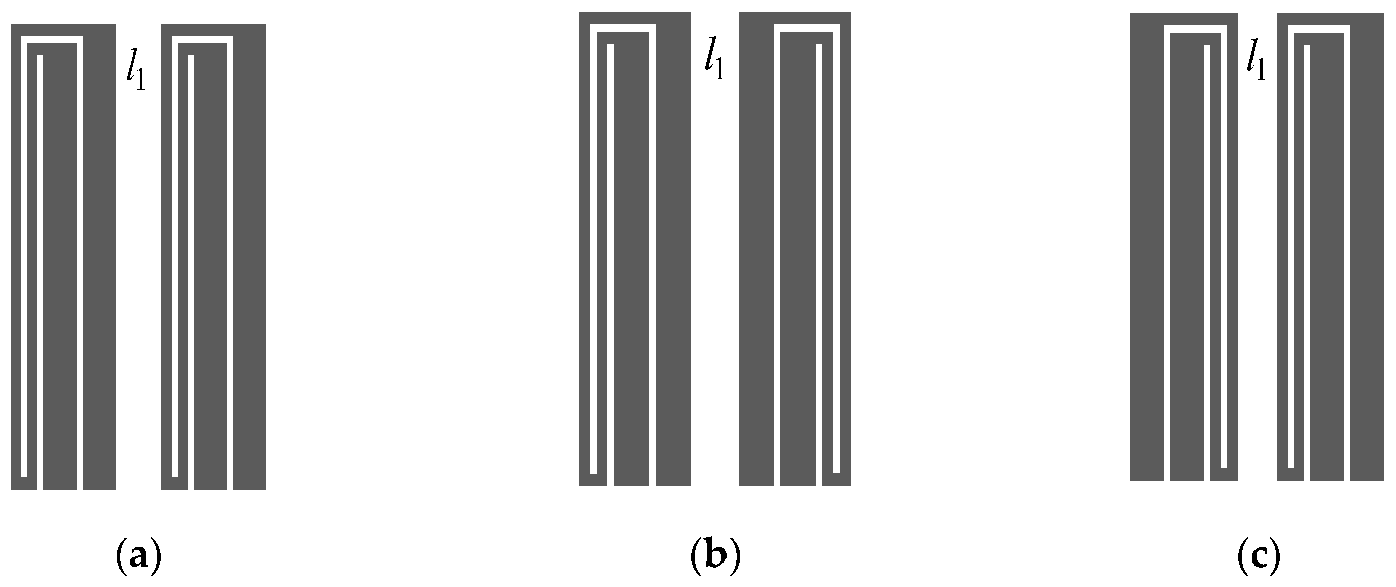
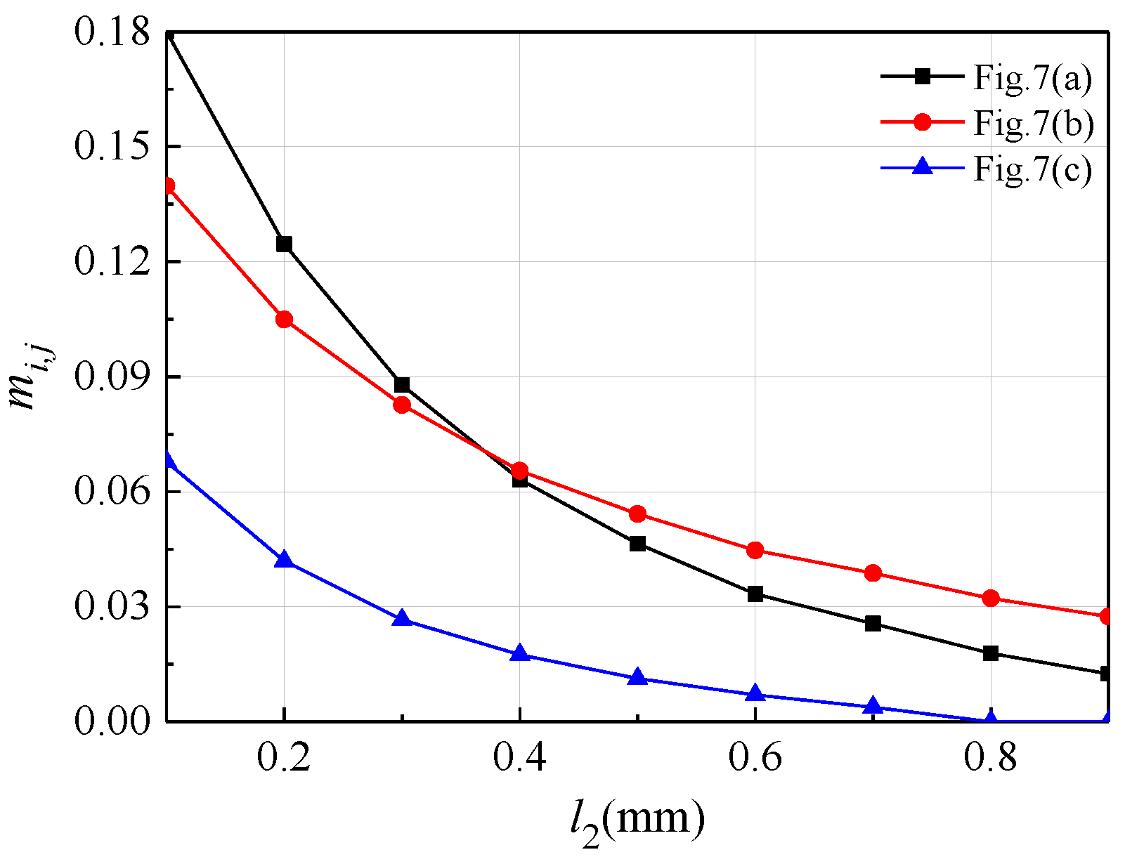
3.2. Analysis of the Internal Coupling Structure

According to the theory presented in [15], the coupling coefficient is determined by the interaction of electrical and magnetic coupling, as shown in Equation (10). Therefore, when electric field coupling and magnetic field coupling offset each other, the resonator can achieve weak coupling, which is conducive to the design of the narrowband or ultra-narrowband filters, for example, the paper [16]. On the contrary, if the electric and magnetic field coupling are separated, the resonator can achieve strong coupling from the electric or magnetic field. In addition, reducing the length of the coupling circuits opposite each other between resonators can weaken the coupling between resonators; on the contrary, the coupling between resonators can be enhanced.
M i , j = M c E c   or   M i , j = E c M c
m i , j = f p 2 2 f p 1 2 f p 2 2 + f p 1 2
The coupling strength between the two resonators should be reduced to quickly reduce the distance between them for the narrow band of Channel I of the HTS diplexer. To change the internal electric field and reduce the length of the front-to-face coupling, a hairpin SIR (HSIR) is designed by deforming the half wavelength resonator, as shown in Figure 4, where the slot width between the micro-strip lines is 0.15 mm in the resonator. The resonator can be composed of three coupling structures, respectively. The couplings in Figure 4 are the electromagnetic hybrid coupling of in-order structure, the electrical coupling of face-to-face structure, and the magnetic coupling of back-to-back structure. The coupling coefficient mi,j between them can be calculated by circuit simulation according to Equation (11), where fp1 and fp2 are the resonant frequencies of the transfer function, respectively [17]. The relation of the coupling coefficient mi,j between resonators of type I varies with their distance l1, as shown in Figure 5. It can be seen that in-order and face-to-face structures can achieve weak coupling, so they are more suitable for the design of narrowband Channel I. In addition, the middle position of the micro-strip line in the HSIR can face outside, which is conducive to realizing direct coupling of the external. It is particularly noted that there is a self-coupling phenomenon inside the resonator, which leads to the resonator’s operating wavelength (λg) being less than the micro-strip line’s actual length (λ1). Thus, the exact micro-strip line length in resonators is greater than 1/2λ1.
For broadband Channel II of the HTS diplexer, OSIR is designed by deforming the half-wavelength resonator to increase the coupling strength between the two resonators, as shown in Figure 6. The electric and magnetic coupling between the two resonators can be fully utilized. The length of the coupling line directly opposite the resonator can be increased for OSIR, wherein the slot width between the micro-strip lines is 0.15 mm in the resonator. The relation of the coupling coefficient mi,j between type II resonators varies with their distance l2, as shown in Figure 7. It can be seen that face-to-face and back-to-back structures can achieve strong coupling, so they are more suitable for designing wideband Channel II. In addition, the middle position of the micro-strip line in the OSIR can face outside, which is conducive to realizing the direct coupling of the external.

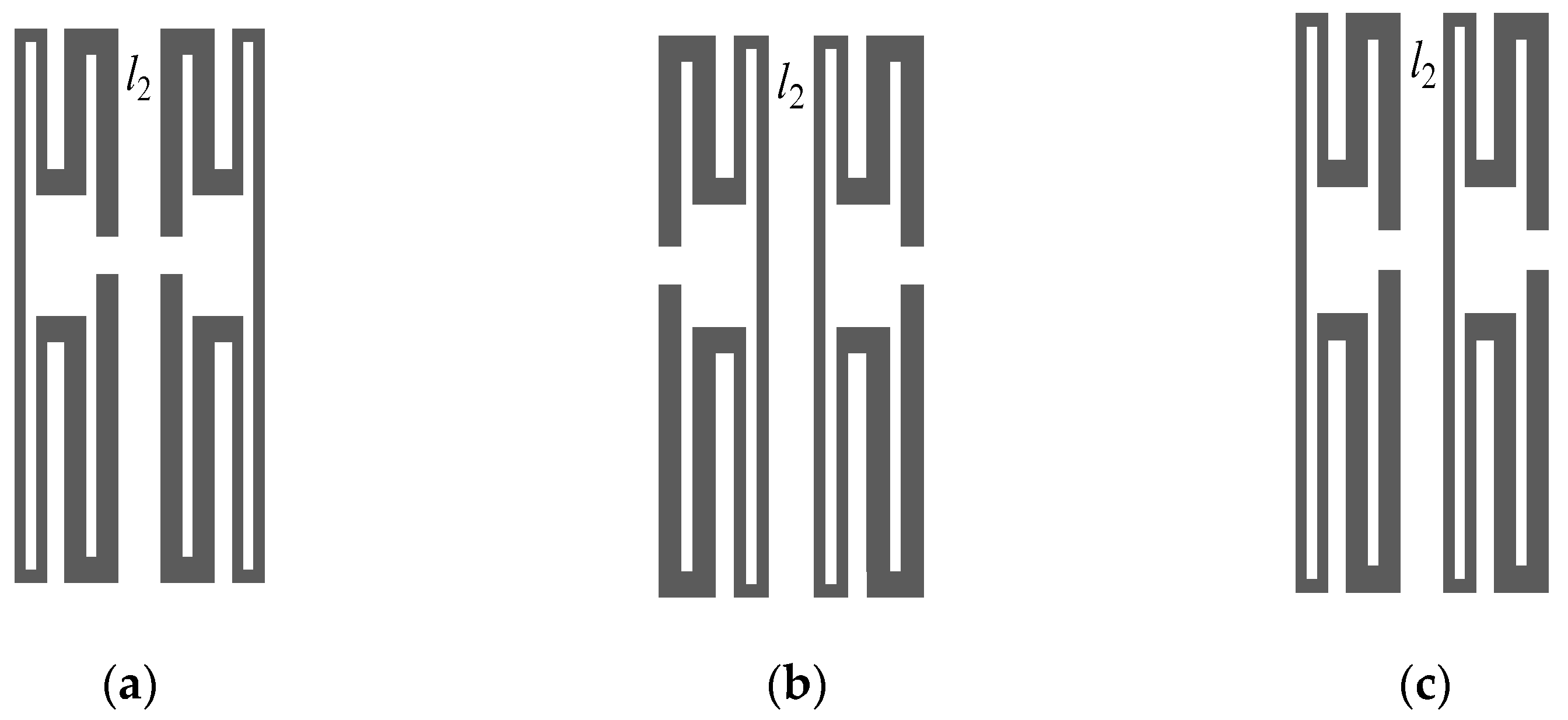
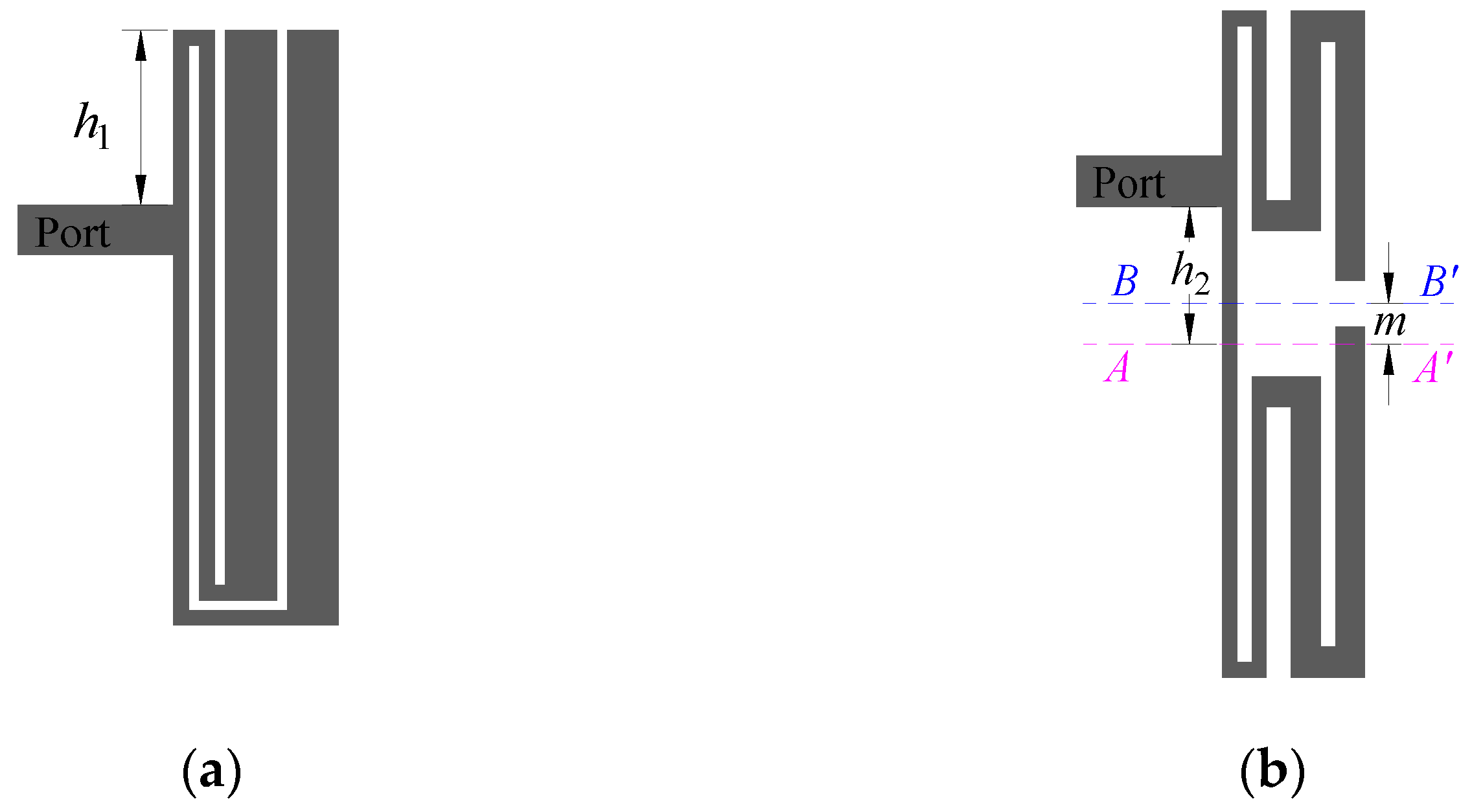
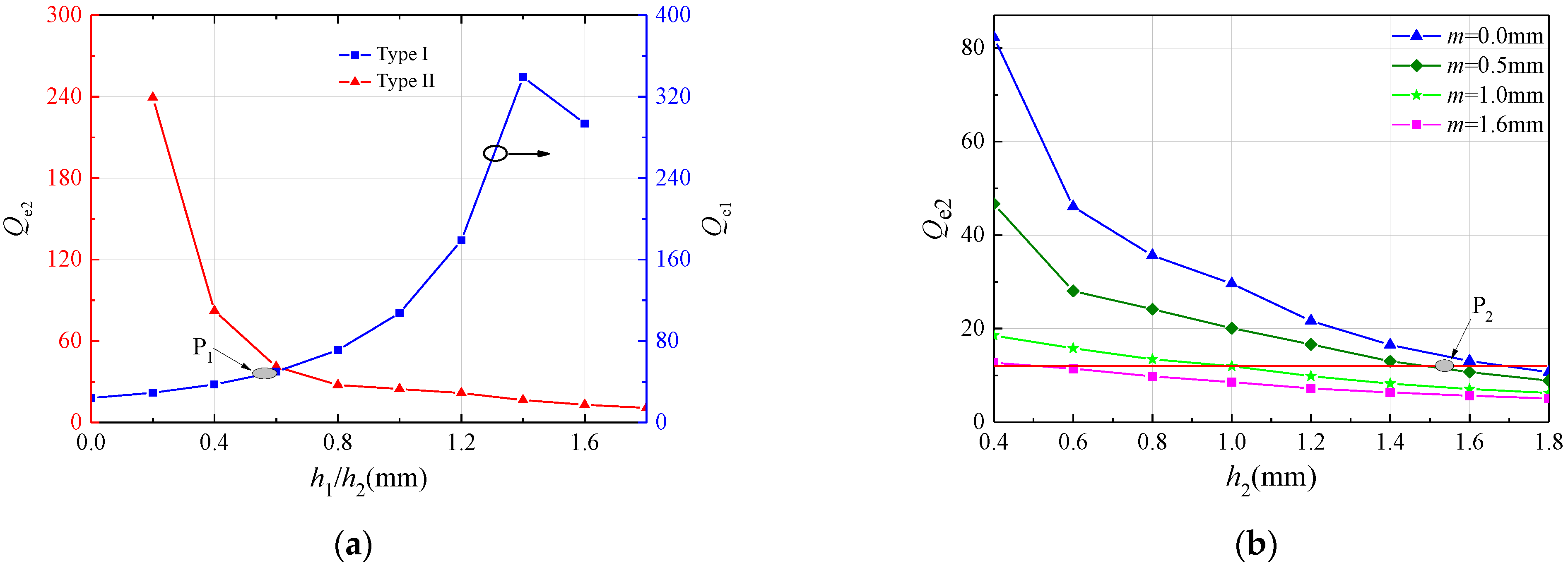
3.3. Analysis of the External Coupling Structure

Based on the two resonators in Figure 4 and Figure 6, the external coupling structure of direct tap feeding in Figure 8 can be constructed. The external quality factor (Qe1/Qe2) in Equation (12) [16] can be calculated by simulating and adjusting the position of the T-junction connected to the resonator with IE3D. The relationship curve between the external quality factor of the type I resonator and h1 can be obtained, and the relationship curve between the external quality factor of the type II resonator and h2 can be obtained, as shown in Figure 9, wherein h1 is the distance from the tapping position to the upper edge of the type I resonator, and h2 is the distance from the tapping position to the symmetrical line (AA’) of the type II resonator. For the resonator of type I, point P1 can be found by adjusting h1, so that the external quality factor meets the requirements of the coupling matrix in filter A. However, for resonators of type II, the external quality factor cannot be obtained by adjusting h2 to meet the requirements of the coupling matrix in Filter B. By adjusting the symmetry planes AA’ to BB’, the OSIR resonance is changed into an asymmetric OSIR structure, so the variable range of the taping position can be widened. When the distance m from AA’ to BB’ takes different values, the change in Qe2 with h2 is shown in Figure 9b. Therefore, a relatively appropriate P2 point (m = 0.5 mm and h2 = 1.55 mm) can be found in Figure 9b, which can meet the requirements of the coupling matrix in Table 3, and the length of Lm1 can be fully utilized.
Q e = ω 0 Δ ω ± 90 o

3.4. Design of the T-Junction

The two band-pass filters in the diplexer introduced in this paper are composed of a T-junction in parallel, as shown in Figure 1. The T-junction design needs to achieve two functions: (1) eliminate the interference between the two passbands and reduce the input reflection at the public port (Port 1); (2) realize external coupling and match the connected passbands. These are the two key factors to the design of the dual-channel diplexer and the difficulties in solving the contradictions, to a certain extent. The two band-pass filters connect with a T-junction and set the length of Lm1 to a quarter of the waveguide wavelength (@fII). At this time, when Channel I (II) operates at the resonant frequency of fI (fII), Channel I (II) is open for Port 2 (3), so signal fII (fI) cannot pass through. Therefore, Port 2 and Port 3 are independent and isolated.
The microstrip line is designed to connect the two band-pass filters with line width W = 0.48 mm (50 Ω @ 1 GHz). According to the iterative optimization method introduced in Part B of Section II, the external quality factor (Qe1/Qe2) in Equation (12) can be calculated by simulating and adjusting the position of the T-junction connected to the resonator with IE3D software. The isolation between the two passbands is improved by adjusting Lm1 and Lm2. At the same time, the access position of the T-junction in the resonator is adjusted repeatedly to achieve a finite filter in-band reflection. Finally, the design of each circuit parameter of the T-junction diplexer is realized. The method effectively solves the interaction between the diplexer channels, but the volumes of Lm1 = 8.84 mm and Lm2 = 12.12 mm obtained from the quarter-wavelength branch circuits are large in the T-junction matching networks. Therefore, it is necessary to reduce the volume of the whole diplexer by improving the T-junction with multiple polylines.

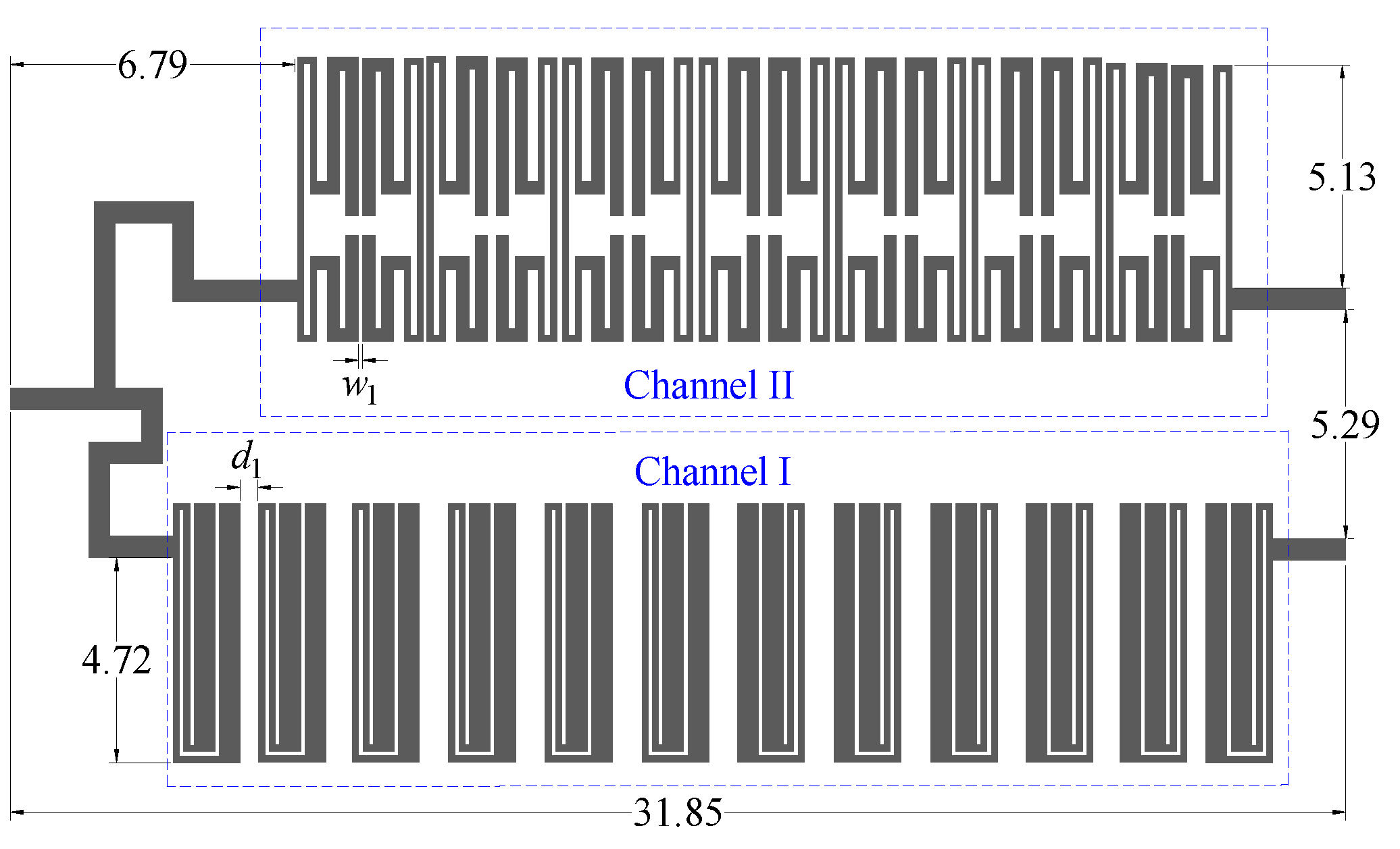
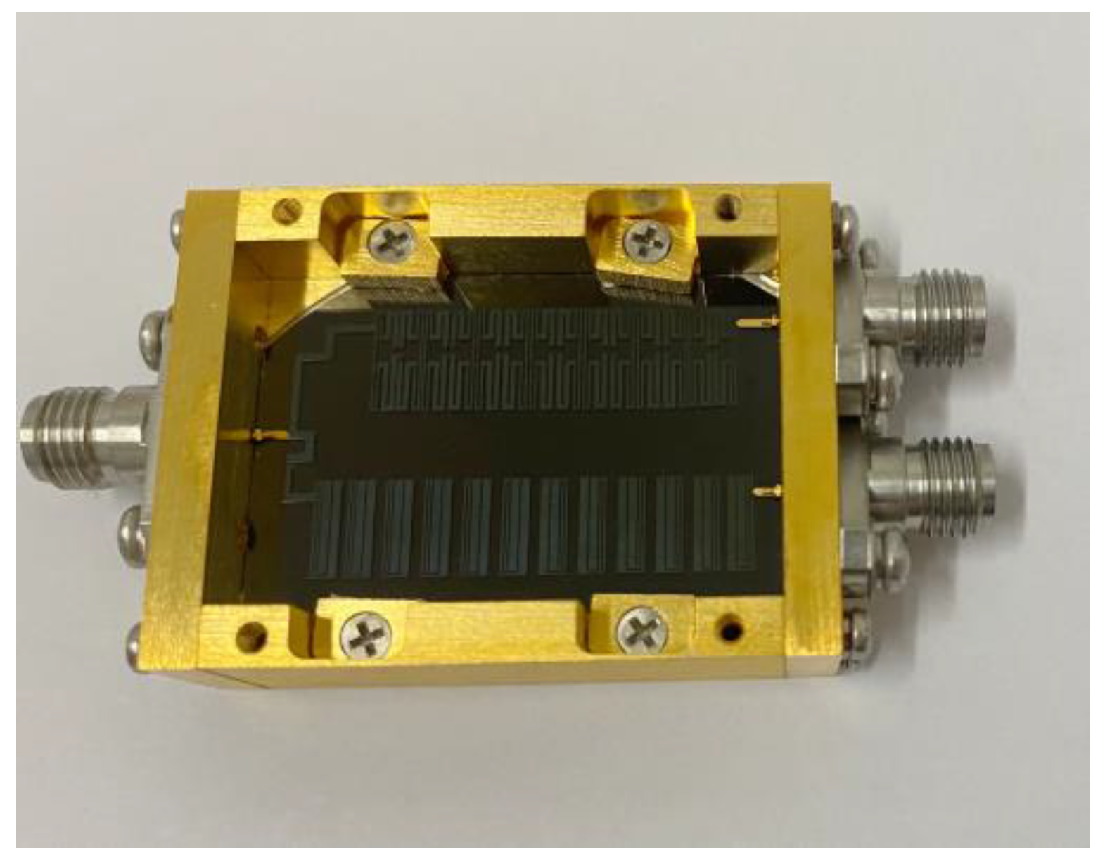
3.5. Design of Circuit Layout

On the YBCO/MGO/YBCO HTS thin film with a thickness of 0.5 mm and dielectric constant of 9.8, the two passband circuits of the diplexer are modeled with the IE3D full-wave electromagnetic simulation software, and based on the coupling coefficient and the external quality factor (Qe1/Qe2) in Table 3. Firstly, the resonator is arranged in an in-order, face-to-face, and back-to-back coupling structure to obtain a rough mode, and then the distance between the two resonators is adjusted according to Equation (11) to obtain the required coupling coefficient [18]. Finite isolation in the passband is obtained by repeatedly changing the Lm1 and Lm2 in the T-junction. At the same time, the zigzag design of the T-junction is carried out to keep the spacing between the two passbands in the minimum range. The external coupling value (Qe1/Qe2) of the two channels can be adjusted by adjusting the insert position of the T-junction. By setting the length of the resonator, the coupling coefficient between resonators, the size of the T-joint, and the access position of the tap as optimization variables, setting reflection, out-of-band suppression, and isolation as optimization objectives in IE3D full-wave electromagnetic simulation software, the size corresponds to the required frequency response obtained through the electromagnetic field analysis and optimization of the software, as shown in Figure 10.
The circuit’s frequency response full-weave electromagnetic simulation (IE3D) is obtained in Figure 11, where the reflection, sideband suppression, and return loss of the two passbands are satisfied with the index requirements and the isolation degree within the two passbands >60 dB. Among them, the in-band isolation degree of Channel II is worse than that of Channel I, indicating that the isolation advantage of the diplexer designed via the T-junction branch matching method in the narrow band is more significant than that in the broadband. Therefore, the T-junction matching structure is suitable for HTS narrowband/ultra-narrowband diplexers.

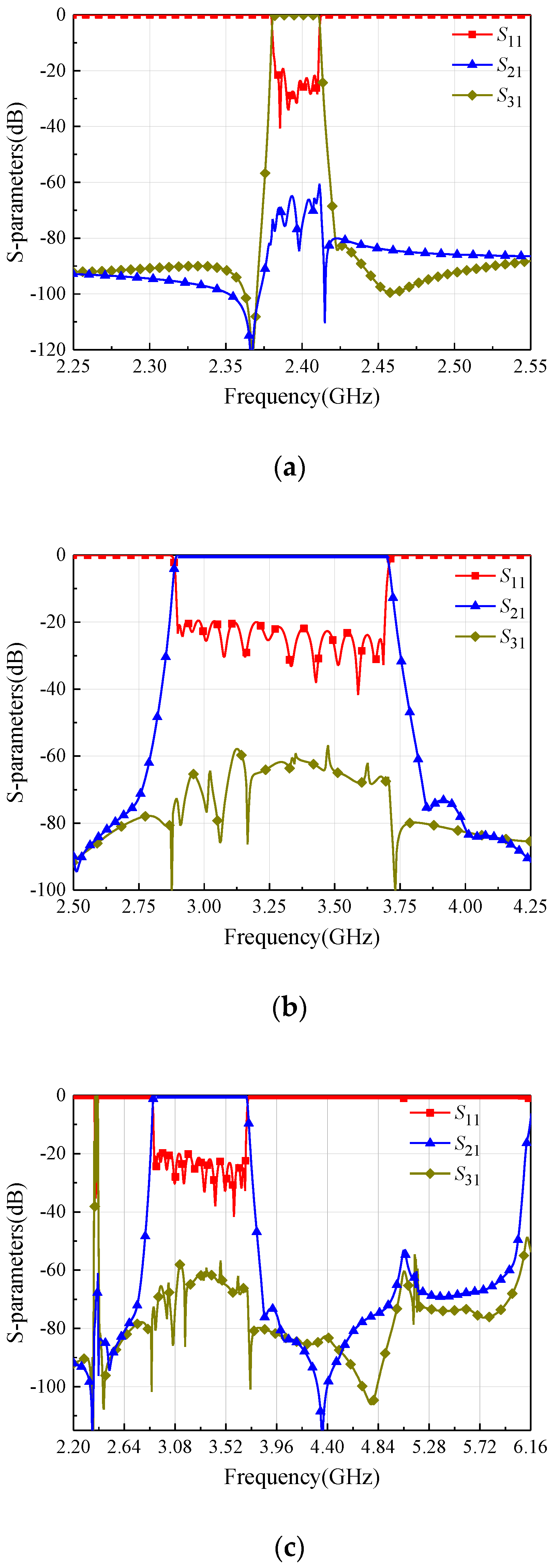
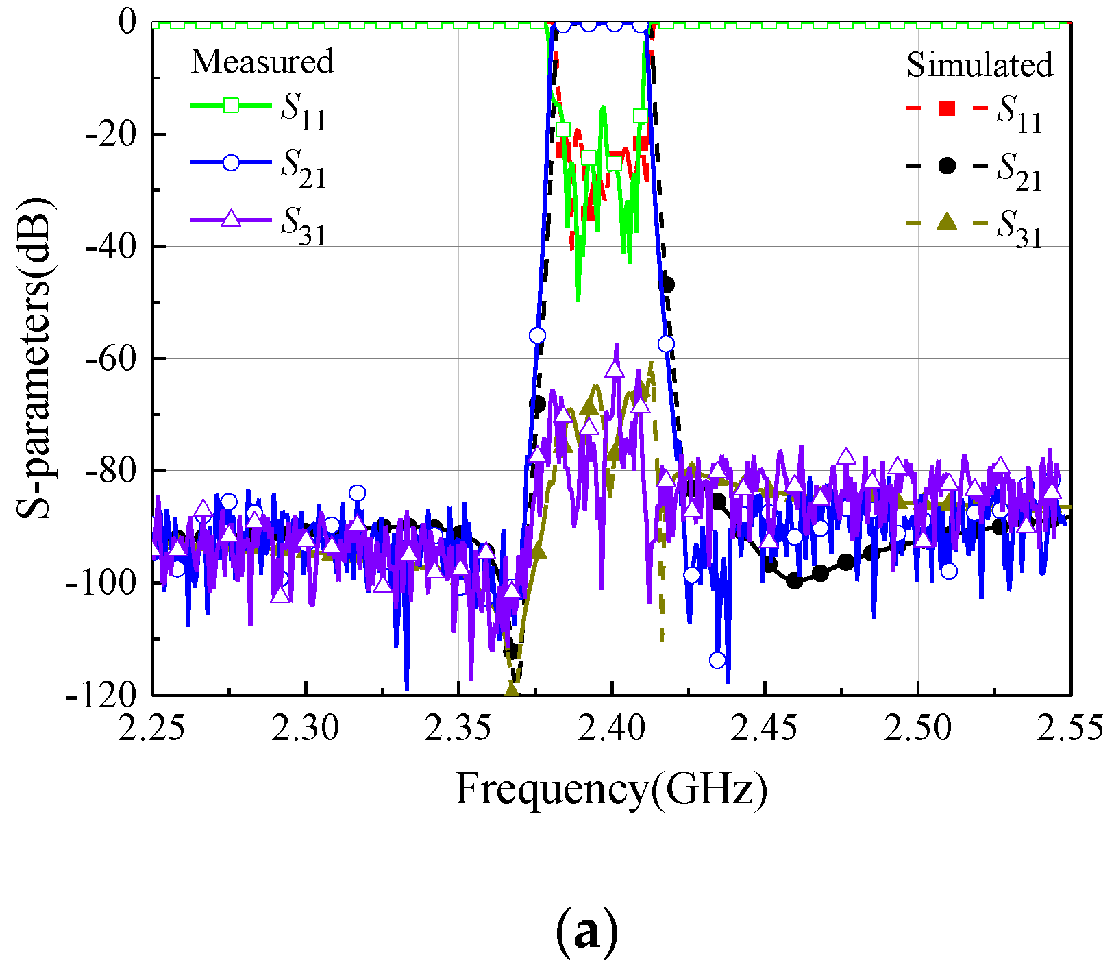
4. Design of HIS Diplexer

One side of the YBCO/MgO/YBCO HTS film with a dielectric constant of 9.8 is etched to obtain a superconducting circuit via high-precision lithography technology and a mask made by the circuit in Figure 10, and the other side is connected with the metal shielding box and is grounded by the bonding circuit. A compact planar structure is adopted in the design process, so the size of the whole diplexer is 31.85 × 17.28 × 0.50 mm3. The physical circuit structure is shown in Figure 12.
The diplexer is measured on the HTS test platform by being fixed onto the copper plate in the Dewar after connecting the insulated cable with the filter connector, turning on the low-temperature cooler, and cooling the diplexer to the superconducting conversion temperature of 77 k. Then, the diplexer’s S-parameters are tested by connecting the vector network analyzer to the test system’s RF input and output terminals. Figure 13 shows the frequency response of the two passbands and the second harmonic of the HTS diplexer measured at low temperatures compared with the EM simulated results. The 3 dB passband coverages are 2378~2410 MHz and 2900~3702 MHz, which have a slight frequency offset compared with the simulation results. In addition, fractional bandwidth (FBW), return loss within the passband, band edge suppression, and isolation within the passband of the HTS diplexer have degraded a little compared with the simulation values, but they can meet the expected index requirements. The measured results compared with the simulation results are shown in Table 4.

5. Conclusions

An HTS diplexer is designed with an SIR resonator, where both channels adopt the simplest high-order Chebyshev filter topology. Taking full advantage of the advantages of HTS thin films, the design of a high-order diplexer with very different FBWs of the two passbands is realized and achieves good sideband suppression, while maintaining a small insertion loss. The physics circuit of the HTS diplexer is designed and measured, and the feasibility of the design method is verified by comparing the simulation and measured results of the diplexer. The HTS diplexer can be well applied in the HTS radar system and can improve the sensitivity and anti-interference ability of the radar system.

Author Contributions

Conceptualization, L.Z., W.Z. and Y.S.; methodology, Y.H., J.J., and D.Z.; software, L.Z.; validation, L.Z., and W.Z.; formal analysis, L.Z. and D.Z.; investigation, L.Z.; resources, L.Z.; writing—original draft preparation, L.Z., and W.Z.; writing—review and editing, L.Z., W.Z. and D.Z.; supervision, L.Z.; project administration, L.Z.; funding acquisition, L.Z. All authors have read and agreed to the published version of the manuscript.

Funding

This work was supported by the National Natural Science Foundation of China under Grant 62201464, the Natural Science Foundation of Sichuan Province under Grant 2022NSFSC0968, and the Natural Science Foundation of Taicang under Grant TC2022JC18.

Data Availability Statement

All data are available from the corresponding author with reasonable request.

Conflicts of Interest

The authors declare no conflict of interest.

References

  1. Hendry, D.R.; Abbosh, A.M. Compact high-isolation base-station duplexer using triple-mode ceramic cavities. IEEE Trans. Ind. Electron. 2018, 65, 8092–8100. [Google Scholar] [CrossRef]
  2. Xie, Y.; Chen, F.C.; Chu, Q.X. Tunable Cavity Filter and Diplexer Using In-Line Dual-Post Resonators. IEEE Trans. Microw. Theory Tech. 2022, 70, 3188–3199. [Google Scholar] [CrossRef]
  3. Wu, Y.; Wu, H.; Wang, W.; Yang, Y.; Lai, Z.; Yang, Q. A Compact Low-Loss High-Selectivity Excellent-Isolation FBAR Duplexer Integrated Chip for LTE Band-3 Industrial Applications. IEEE Trans. Circuits Syst. II Express Briefs 2022, 69, 4563–4567. [Google Scholar] [CrossRef]
  4. Tian, H.; Chen, Z.; Chang, L.; Wang, R.; Wang, S.; Liu, H.; Du, C.; Zhou, D.; Ma, Z. Differentially Fed Duplex Filtering Dielectric Resonator Antenna With High Isolation and CM Suppression. IEEE Trans. Circuits Syst. II Express Briefs 2021, 69, 979–983. [Google Scholar] [CrossRef]
  5. van Liempd, B.; Visweswaran, A.; Ariumi, S.; Hitomi, S.; Wambacq, P.; Craninckx, J. Adaptive RF front-ends using electrical-balance duplexers and tuned SAW resonators. IEEE Trans. Microw. Theory Tech. 2017, 65, 4621–4628. [Google Scholar] [CrossRef]
  6. Psychogiou, D.; Gómez-García, R.; Peroulis, D. Tune-all RF planar duplexers with intrinsically switched channels. IEEE Microw. Wirel. Compon. Lett. 2017, 27, 350–352. [Google Scholar] [CrossRef]
  7. Park, J.; Jin, S.; Moon, K.; Kim, B. Wide-band duplexer based on electrical balance of hybrid transformer having two notches. Electron. Lett. 2016, 52, 1151–1153. [Google Scholar] [CrossRef]
  8. Li, C. Recent progress of superconducting electronics in China. Acta Phys. Sin. 2021, 70, 184–209. [Google Scholar] [CrossRef]
  9. Wang, L.T.; He, M.; Xiong, Y.; Zhang, W.; Chen, H.-H.; Ji, L. Design of high selectivity narrowband eight-order high-temperature superconducting sextaplexer. Supercond. Sci. Technol. 2020, 33, 115016. [Google Scholar] [CrossRef]
  10. Kuroda, A.; Saito, A.; Ohshima, S. Design and Fabrication of Compact HTS Duplexers Using a CQ Structure With a High Qu Resonator. IEEE Trans. Appl. Supercond. 2014, 25, 1–4. [Google Scholar] [CrossRef]
  11. Xu, Z.; Jingping, L.; Shaolin, Y.; Lan, F.; Bo, Z.; Xinjie, Z. Miniaturized high-temperature superconducting multiplexer with cascaded quadruplet structure. Supercond. Sci. Technol. 2015, 28, 065016. [Google Scholar] [CrossRef]
  12. Cameron, R.J.; Harish, A.; Radcliffe, C.J. Synthesis of advanced microwave filters without diagonal cross-couplings. IEEE Trans. Microw. Theory Tech. 2002, 50, 2862–2872. [Google Scholar] [CrossRef]
  13. Guan, X.; Gui, P.; Ren, B.; Zhang, X. Compact quad-channel high-temperature superconducting diplexer based on stub-loaded square ring resonator. Int. J. RF Microw. Comput.-Aided Eng. 2019, 29, e21725. [Google Scholar] [CrossRef]
  14. Yue, H.; Tang, H.; Wang, L.; Gong, L.; Li, C.; Wei, B.; Xie, Q.; Duan, J. Design of miniature high-temperature superconducting quadruplexer with wide stopband suppression. Phys. C Supercond. Its Appl. 2020, 579, 1353735. [Google Scholar] [CrossRef]
  15. Zhou, L.G.; Zhang, W.; Wong, P.K.J.; Bai, X.D.; Long, Z.H.; Zhang, T.L. Synthesis and design of asymmetric cul-de-sac structure HTS filter with transmission zero introduced in Pairs. Supercond. Sci. Technol. 2022, 35, 115004. [Google Scholar] [CrossRef]
  16. Zhou, L.; Li, H.; Long, Z.; Wu, H.; Zhang, T.; Qiao, M. Novel configuration of a HTS filter with adjustable transmission zeros based on a modified cascaded quartet structure. Supercond. Sci. Technol. 2018, 31, 085008. [Google Scholar] [CrossRef]
  17. Teng, Z.; Zhong, L.; Chen, G.; Zhou, T.; Gong, L.; He, M.; Zhang, X. Design of extensible superconducting multiplexer with modular structure to overcome the limit of wafer size. Phys. C Supercond. Its Appl. 2020, 578, 1353736. [Google Scholar] [CrossRef]
  18. Zhou, L.; Long, Z.; Wu, H.; Han, Y.; Li, H.; Zhang, T. Design of special asymmetric cul-de-sac unit configuration high temperature superconductor filter with multi-pair of transmission zeros. Supercond. Sci. Technol. 2020, 33, 085006. [Google Scholar] [CrossRef]
Figure 1. Schematic diagram of the T-junction diplexer.
Electronics 12 00691 g001
Figure 2. Schematic diagram of source complex admittance.
Electronics 12 00691 g002
Figure 3. SIR resonator. (a) Planar circuit; (b) equivalent circuit.
Electronics 12 00691 g003
Figure 4. Coupling structure between the resonators of type I. (a) In order; (b) face to face; (c) back to back.
Electronics 12 00691 g004
Figure 5. Coupling coefficient between the resonators of type I.
Electronics 12 00691 g005
Figure 6. Coupling structure between resonators of type II. (a) Face to face; (b) back to back; (c) in order.
Electronics 12 00691 g006
Figure 7. Coupling coefficient between the resonators of type II.
Electronics 12 00691 g007
Figure 8. The resonator with port. (a) Type I; (b) type II.
Electronics 12 00691 g008
Figure 9. The external quality factor of the diplexer. (a) Qe1 (Qe2) with different h1(h2); (b) Qe2 with different h2 when m definite.
Electronics 12 00691 g009
Figure 10. The layout of the HTS diplexer.
Electronics 12 00691 g010
Figure 11. The simulation frequency response of the diplexer. (a) Channel I; (b) Channel II; (c) broadband.
Electronics 12 00691 g011
Figure 12. Fabricated HTS diplexer.
Electronics 12 00691 g012
Figure 13. The measured and simulated frequency response of the HTS diplexer. (a) Channel I; (b) Channel II; (c) broadband.
Electronics 12 00691 g013aElectronics 12 00691 g013b
Table 1. Index of the filter.
Filter AFilter B
Passband bandwidth (MHz)2380~24102900~3700
Insert loss (dB)≤0.2≤0.2
Fractional bandwidths (%)1.2524.24
Out-of-band suppression (dB)≥80≥70
Order of filter1214
Return loss (dB)≤−20≤−20
Parasitic passband (GHz)≥5.2 GHz≥6.6 GHz
Ratio of f1/f0≥2.2≥2
Table 2. The coupling coefficient of the filter.
FilterCoupling Coefficient
Am1,2m2,3m3,4m4,5m5,6m6,7
0.01640.00910.00740.00700.00690.0068
m7,8m8,9m9,10m10,11m11,12Q
0.00690.00700.00740.00910.016446.95
Bm1,2m2,3m3,4m4,5m5,6m6,7
0.19710.14050.13050.12720.12600.1256
m7,8m8,9m9,10m10,11m11,12Q
0.12600.12720.13050.14050.197113.47
Table 3. The coupling coefficient of the diplexer.
ChannelCoupling Coefficient
Im1,2m2,3m3,4m4,5m5,6m6,7
0.01490.00920.00790.00750.00730.0071
m7,8m8,9m9,10m10,11m11,12Q
0.00710.00730.00770.00890.015446.19
IIm1,2m2,3m3,4m4,5m5,6m6,7
0.20010.14040.13220.12860.12750.1268
m7,8m8,9m9,10m10,11m11,12Q
0.12700.12850.13140.14040.195512.24
Table 4. Simulated and measured response of the diplexer.
SpecificationsSimulatedMeasured
Channel I (MHz)2379~24112378~2410
Channel II (MHz)2898~37012900~3702
Out-of-band rejection (dB)82/8080/80
Insertion loss (dB)0.08/0.090.11/0.12
Return loss (dB)−21/−21−16/−15
Band-edge steepness (dB/MHz)9.9/2.29.7/2.3
Isolation (dB)62/6059/57
Parasitic passband (GHz)2.2/2.02.2/2.0
Disclaimer/Publisher’s Note: The statements, opinions and data contained in all publications are solely those of the individual author(s) and contributor(s) and not of MDPI and/or the editor(s). MDPI and/or the editor(s) disclaim responsibility for any injury to people or property resulting from any ideas, methods, instructions or products referred to in the content.

