Article

Asymmetric 5.5 GHz Three-Stage Voltage-Controlled Ring-Oscillator in 65 nm CMOS Technology

Dipartimento di Ingegneria dell’Informazione, Università di Pisa, 56122 Pisa, Italy
*
Author to whom correspondence should be addressed.
Electronics 2023, 12(3), 778; https://doi.org/10.3390/electronics12030778
Submission received: 5 January 2023 / Revised: 28 January 2023 / Accepted: 1 February 2023 / Published: 3 February 2023
(This article belongs to the Special Issue Feature Papers in Circuit and Signal Processing)

Abstract

:
The current trend of increasing the complexity of hardware accelerators to improve their functionality is highlighting the problem of sharing a high-frequency clock signal for all integrated modules. As the clock itself is becoming the main limitation to the performance of accelerators, in this manuscript, we present the design of an asymmetric Ring Oscillator-Voltage-Controlled Oscillator (RO-VCO) based on the Current Mode Logic architecture. The RO-VCO was designed on commercial-grade 65 nm CMOS technology, and it is capable of driving large capacitance loads, avoiding the need for additional buffers for clock-trees, reducing the silicon area and power consumption. The proposed RO-VCO is composed of three closed-loop differential and asymmetrical stages, and it is able to tune the working frequency in the range from 4.72 GHz to 6.12 GHz. The phase noise and a figure of merit of −103.2 dBc/Hz and −186 dBc/Hz were obtained at 1 MHz offset from the 5.5 GHz carrier. In this article, the analytical model, full custom schematic, and layout of the proposed RO-VCO are presented and discussed in detail together with the experimental electrical and thermal characterization of the fabricated device.

1. Introduction

The increasing need for multi-scale simulations to achieve realistic results of complex physical processes, along with the accurate management of image processing and the analysis of critical real-time applications, is the driving force behind the huge request for multicore processors and accelerators [1,2]. They can be composed of several processor cores attached to hardware accelerators and memories for performance enhancement of parallel computation and multithreading. Every single unit shares common buses and caches, which can be the critical part of the system performance if not properly managed [3].
The shared bus that connects the growing number of cores suffers from scalability problems, and adding new blocks requires redesigning the whole system [4,5]. Moreover, the high number of interconnected gates increases the power consumption of the local clock distribution net. The global clock distribution network should be buffered to allow the clock signal to reach all the units connected to the shared bus even if an inevitable delay is added in the path.
The Network on a Chip approach, based on synchronous links, seems to be a solid solution to reduce the power consumption and increase the bandwidth. Clock management is accomplished by generating a clock in a region of the system and distributing it via a complex clock-tree that reduces the signal latency and increases fan-out. A symmetric structure should be provided by the clock-tree in order to facilitate the design of the branch structures with a controlled capacitance and inductance [6]. In general, the number of clock-tree stages is a function of the number of points of load and of the clock-source’s ability to drive large-capacitance loads (high fan-out). For this reason, a clock source with a high fan-out is attractive to simplify the clock-tree and for the optimization of the buffer and wire sizes [7].
The most widely used system for generating the clock signal within an integrated system is the Phase-Locked Loop [8,9]. This system makes it possible to stabilize the high-frequency signal generated by a Voltage-Controlled Oscillator (VCO) with a very precise reference signal, but with a frequency that is too low for the application. Focusing on the VCO, there are various types of oscillators that can vary their oscillation frequency depending on an electrical quantity. In particular, there are two types of VCOs that are most commonly used for their ability to reach high frequencies with good performance: VCOs relying on the operation of the Inductance–Capacitance resonant group combined with a gain stage capable of balancing the tank’s resistive losses; VCOs based on Ring Oscillators (ROs), where the signal is fed back with the proper phase and amplification. Comparing the two solutions, the first offers better performance in terms of phase noise and robustness to process, temperature, and voltage variations, but at the cost of a larger area [10,11]. The second solution, on the other hand, enables the design of very compact systems with reduced performance [12,13,14]. Considering the area cost of the more advanced process usually adopted to design hardware accelerators, the second solution is typically preferred for the generation of clock signals [15,16]. For this reason, in this paper, we propose the design of an asymmetric RO-VCO capable of driving large capacitance loads, yet avoiding the need for additional buffers for clock-trees and reducing latency, area, and power consumption. Thermal tests were also conducted on the manufactured chip in order to investigate its behavior with increasing temperatures, thus evaluating the impact of thermal effects on the RO-VCO during normal multicore operation.
Concerning the paper organization, Section 2 presents the model of the proposed RO-VCO with the extraction of the main design parameters and their impact on the final performances. The schematic design of the whole RO-VCO and that of each single cell is reported in Section 3. Section 4 concerns the RO-VCO layout with the description of the solutions adopted to face the high-temperature issues. The analysis of the collected data from the electric and thermal characterization is discussed in Section 5. The comparison with the state-of-the-art is made in Section 6, and conclusions are drawn in Section 7.

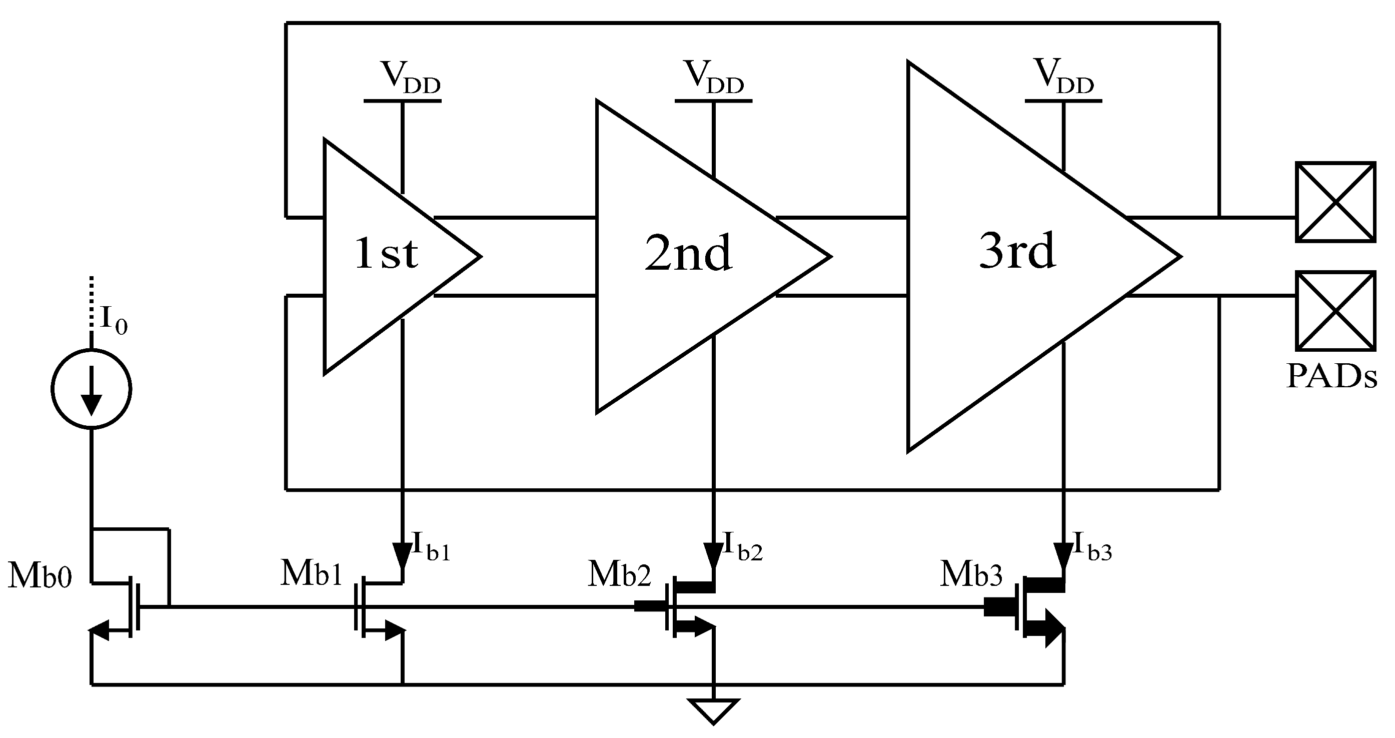
2. System Model of the Proposed RO-VCO

One solution to simplify the clock-tree design, reducing its area and power consumption, is the increment in the VCO driving capability: the greater its strength, the lower the number of cascaded stages in the clock-tree. Typically, the classical architecture of the RO-VCO is composed of all equal stages connected to several buffers to increase the VCO driving capability [17,18,19]. In this work, we propose to increase the driving capability of the RO-VCO, which in turn allowed us to remove the cascading buffers. Following this approach, we modeled a generic N-stage RO-VCO, where each stage features a size increment factor K, similar to a tapered factor chain. The model of the proposed controlled oscillator is depicted in Figure 1 for the case N = 3. Each stage in the loop is composed of an amplifier, an equivalent resistance that represents the previous stage’s output resistance, and an equivalent capacitance representing the input capacitance of the following stage, as well as the variable capacitance due to the varactors used to control the oscillation frequency. In addition, the loading capacitor C L connected to the output of the last stage models the following loading stage.
From the first to the last stage of the loop, the gain of each amplifier, represented by the transconductance g m , increases by a factor K, while the equivalent resistance R decreases by the same factor through the loop. Consequently, the equivalent capacitance C scales with the transconductance stages.
Defining the parameters ω 0 = 1 / ( R C ) and α = ( C + C L ) / C and considering a generic number of stages N, the loop-gain of the whole system can be expressed by Equation (1).
F ( s ) = ( K 2 g m R ) N ( 1 + s α ω 0 ) ( 1 + s K 3 ω 0 ) N 1
Theoretically, considering the Barkhausen criterion on the module and phase, it is possible to derive the oscillation frequency and the gain condition to design the oscillator. However, since no close equation form that includes all parameters N, K, ω 0 , and α can be derived, the analytical expression should be resolved for each selected number of stages separately. For example, considering the case of a three-stage RO-VCO, the conditions on the oscillation frequency and on the gain required to start up and sustain the oscillation are reported in Equations (2) and (3), respectively, where ω p is the oscillating pulsation.
ω P = ω 0 2 K 3 + α α K 6
g m R 1 K 3 2 α ( K 3 + α ) 2 3
By replacing α = 1 and K = 1, we obtained ω P = ω 0 3 and g m R 2 , which are the classic conditions obtained for a symmetrical three-stage RO-VCO. Comparing the area of the proposed tapered RO-VCO and that of a three-symmetrical-stage RO-VCO working at the same frequency, an area reduction can be achieved. Indeed, the ratio between the area of the asymmetric and the symmetric stages is expressed in Equation (4).
A a s y m A s y m = ( K 2 + K + 1 ) 2 K 3 + α α K 6 3 3
Hypothesizing the use of the Current Mode Logic (CML) cells for the RO-VCO, where the transistor g m is proportional to the tail current, it is possible to estimate the proposed asymmetric RO-VCO power consumption and compare it with that of a symmetric one, as reported in Equation (5).
P C a s y m P C s y m = ( K 2 + K + 1 ) 2 ( K 3 + α ) 2 α 3 6 K 3
A graphical representation of the area and power ratio is depicted in Figure 2 for better visualization. At first glance, the reduction of the area and power ratio would suggest working with high K and α , but on closer inspection, several factors limit the gain of this solution.
Indeed, given a target frequency, the higher the K and α , the higher should be the ω 0 , which is, however, limited by the technological parameters and the voltage swing required by the application. Therefore, since advanced technologies allow for high ω 0 and the working frequency of the computing unit can be limited to a few GHz, instead of ballasting the RO-VCO with additional capacity or increasing the size of all stages in a symmetric way, the factors K and α can be increased to improve the RO-VCO’s drive capability. In this work, considering a 65 nm technology and a targeted frequency of 5.5 GHz, a three-stage RO-VCO with K = 2 and α = 18.8 is fully custom designed.

3. Schematic Design of the RO-VCO

The proposed controlled oscillator is composed of three differential and asymmetrical CML cascaded buffer stages, which are biased with a simple sink current mirror, as shown in Figure 3. The current I 0 biases the MOSFET M b 0 connected as a diode and is mirrored in M b 1 , M b 2 , and M b 3 , following the mirror ratio 1, K, and K 2 , respectively, in accordance with the considerations made in Section 2. The fixed current I 0 is externally provided by off-chip commercial devices. The adoption of a CML architecture improves the RO-VCO robustness to process, temperature, and voltage variations compared to a classic CMOS cell. This helps to reduce the RO-VCO performance drift at high temperatures, such as when multicore processors are overloaded. For the purposes of the electrical experimental test performed to assess the ability of the proposed RO-VCO to drive a large load, this is represented by the chip pads, rather than the input stage of a clock-tree. This way, we avoided the necessity of designing an additional buffer to measure the signal with out-of-chip instrumentation.
As illustrated in Figure 4, each stage of the oscillator is a CML buffer consisting of a MOSFET couple, a tail current mirror, and two pull-up resistors, where x indicates the generic x th stage of the RO-VCO we are referring to [20]. In addition, a varactor couple is connected to the outputs of each stage to allow for the fine-tuning of the frequency of the controlled oscillator.
Targeting an oscillation frequency of 5.5 GHz and a load capacitance of 350 fF, we selects K = 2 and α = 18.8 by some simulative iterations. With these values, we obtained C = 28 f F and R = 160 Ω , which allowed us to achieve a good tradeoff between area and power consumption. Following these criteria, the first cell of the RO-VCO was sized by choosing a width of the MOSFET couple (M1) of 24 µm and pull-up resistors of 640 Ω .
As reported in Table 1, the other device sizes were scaled by the factors K and K 2 following the model relationship reported in Section 2. The MOSFET devices Mx in the source coupled differential pair were designed with the minimum channel length allowed by technology. Although this approach increases the effects of the process variations of the whole system, it allows increasing the parameter ω 0 of the RO-VCO model in Section 2, enabling the use of higher K and α values. Instead, the MOSFETs in the tail current mirror were designed with the maximum channel length allowed by the transistor model to increase their output resistance, and their widths were designed to bias the MOSFETs in the saturation region and provide the proper bias currents in each stage.
Figure 5 depicts the schematic of the three-stage RO-VCO presented in this paper.

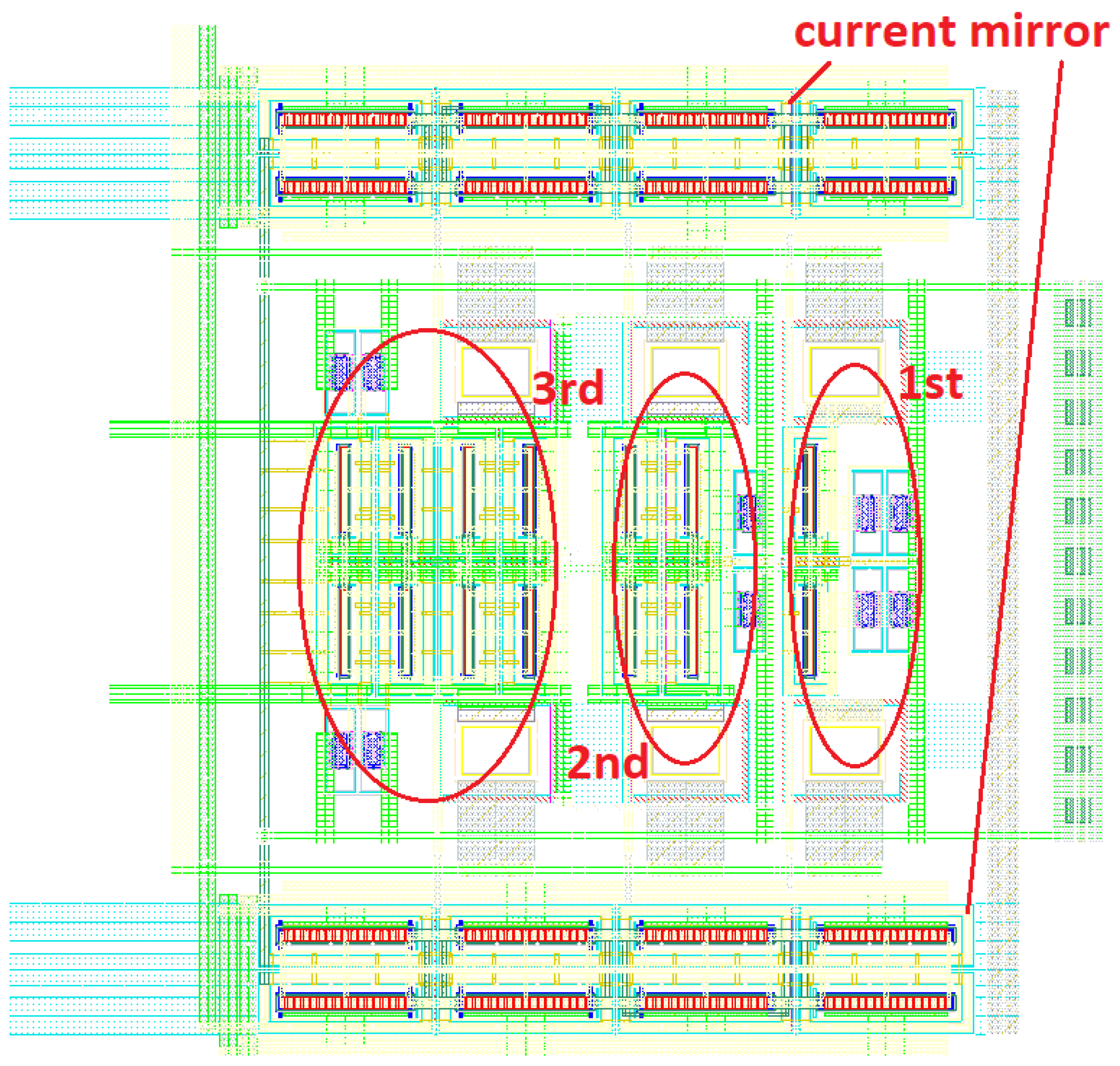
4. Layout Design of the RO-VCO

The layout of the RO-VCO is based on a full-custom approach. For matching purposes, all resistors and MOSFETs were manufactured with an interdigitated structure and a common centroid approach. MOSFETs with several fingers were used to reduce the series gate resistance and provide a compact layout. Considering the targeted application, where the RO-VCO is integrated into high-performance computers, whose cores can operate at high temperatures when overloaded, one of the main challenges in the layout is related to the metal path electromigration, which poses limitations on the metal widths and via numbers. For example, to avoid electromigration phenomena, the maximum current density in the metal paths and vias must be reduced by a factor of 8.8 when passing from 85 °C to 125 °C. Therefore, while wide metals are needed to avoid electromigration phenomena, they lead to large parasitic capacitances. As a result, for each metal connection, a trade-off between the maximum operating temperature and overall load capacitance must be chosen. The layout of the proposed RO-VCO is depicted in Figure 6. On the top and bottom sides, a simple current mirror is implemented, and in the middle, from left to right, the third, second, and first stages of the controlled oscillator are designed with their respective resistors and varactors. The total layout area of the proposed RO-VCO is 87 × 115 µm2.

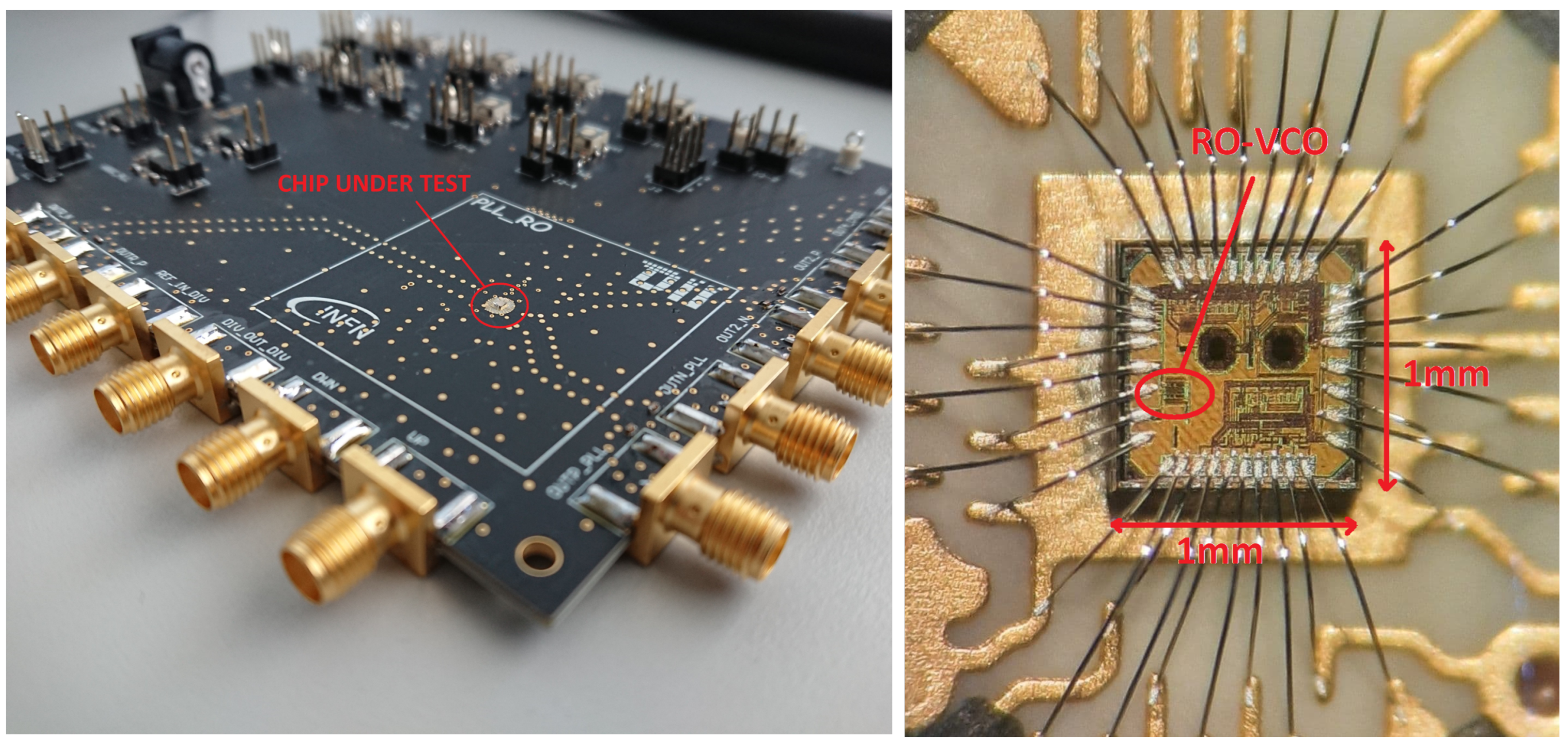
5. Experimental Characterization

The experimental characterization of the RO-VCO was performed by gluing the fabricated chip directly on a high-speed testing board specially designed for the test of the devices hosted in the chip. The connection between the chip pads and board traces were made with 35 µm aluminum wire bonds.
Figure 7 (left) shows the testing board with the bonded chip and the commercial devices needed for testing purposes, such as the bias current generator ( I 0 in Figure 3 and Figure 5) and supply voltage generator, as well as the high-speed connectors.
A zoom in of the 1 mm2 chip hosting the proposed RO-VCO inside the red circle is shown in Figure 7 (right). The other shapes are the components of another experimental device not discussed in this paper.

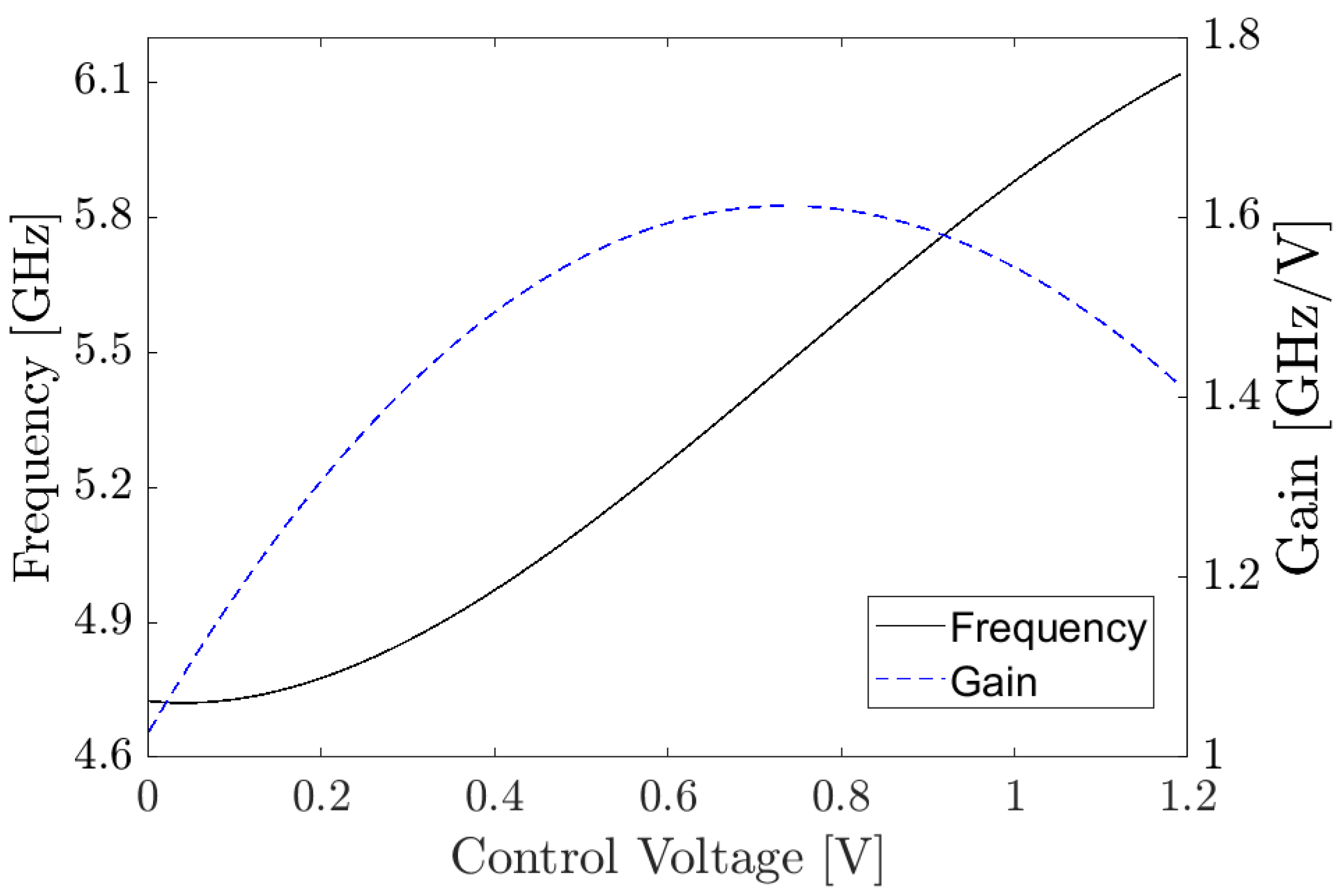
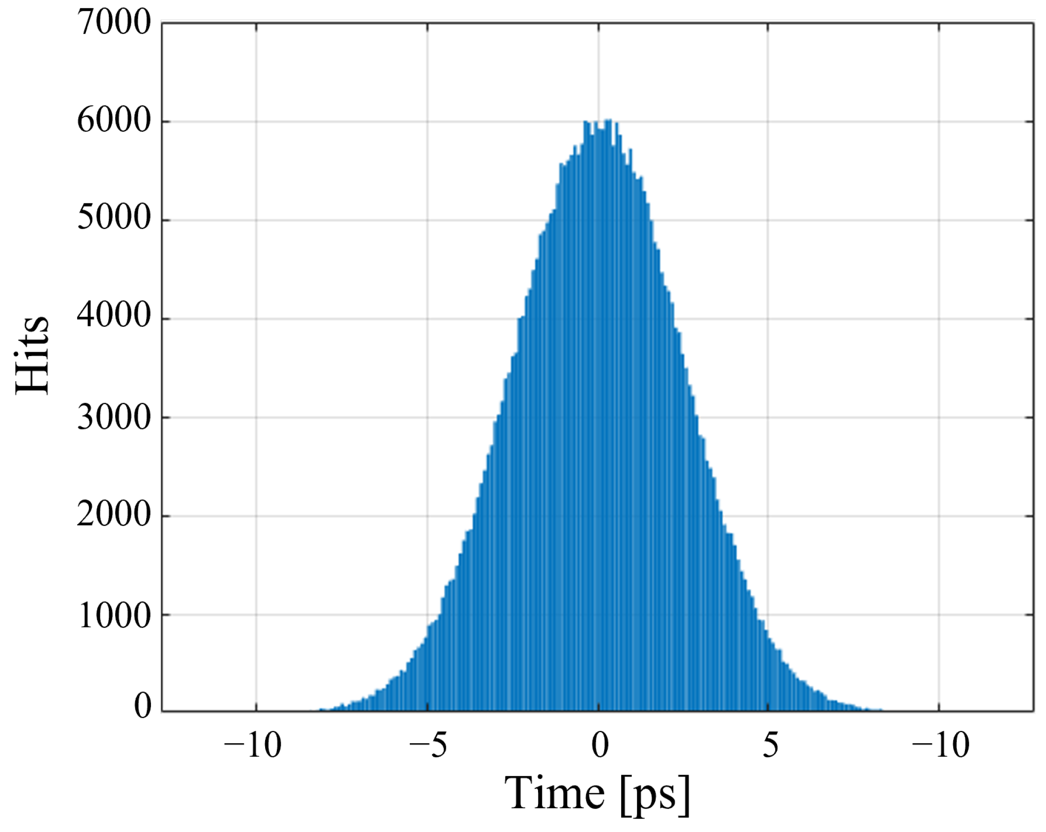
5.1. Electrical Characterization

Frequency domain measurements were performed with the Rohde&Schwarz FSL18 Spectrum Analyzer, connecting the RO-VCO differential outputs to the single-ended spectrum analyzer input through a Marki microwave balun (Bal-0036). Figure 8 depicts the RO-VCO output signal spectrum centered around 5.5 GHz for a control voltage equal to 0.751 V.
In Figure 9, the black solid line depicts the measured free-running frequency of the oscillator as a function of the control voltage, showing a tuning range from 4.72 GHz to 6.12 GHz. In addition, the RO-VCO gain as a function of the control voltage is shown with the blue dotted line. For the experimental characterization of the proposed RO-VCO, the control voltage is provided by an external off-chip device capable of covering the entire range from 0 V to V D D . It should be noted that, in a system application where the RO-VCO is integrated into a complete PLL, the control voltage is provided by the PLL itself to lock the RO-VCO output signal in phase with a precise reference signal. The 5.5 GHz target frequency was achieved with a control voltage equal to 0.751 V, where an oscillator gain of 1.61 GHz/V is exhibited.
A time domain measurement of the RO-VCO output signal for the minimum and maximum control voltage is also shown in Figure 10. It was measured with a 23 GHz 100 GS/s Tektronix mixed-signal oscilloscope. Considering Figure 10, by comparing the trace of the highest control voltage with that of the lowest voltage, time compression and, consequently, an increase in frequency can be observed, as expected.
Using a bias current I 0 = 1.6 mA, the measured power consumption is 15.45 mW, and the phase noise at a 1 MHz distance from the carrier is −103.2 dBc/Hz. The phase noise behavior with the frequency is discussed in the next section along with its behavior with temperature.
In order to give a more meaningful interpretation of the phase noise effect on a digital system, such as a high-performance computer application, the measure of the cycle-to-cycle jitter of the proposed RO-VCO is pictured in Figure 11. It illustrates how much the clock period varies between any two adjacent cycles. The histogram features a mean value of around 0.08 ps with a standard deviation of about 2.11 ps from a population of roughly 350 k samples, where population means the number of individual observations contained in a statistical data collection.

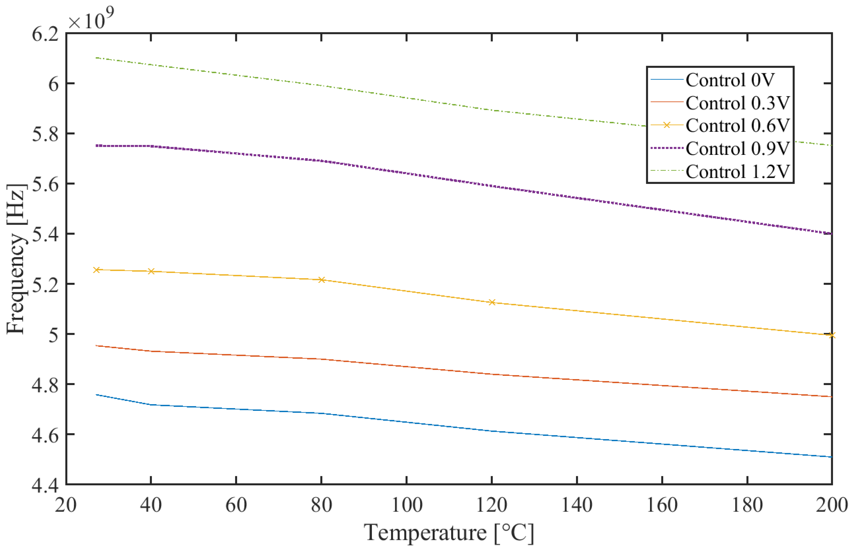
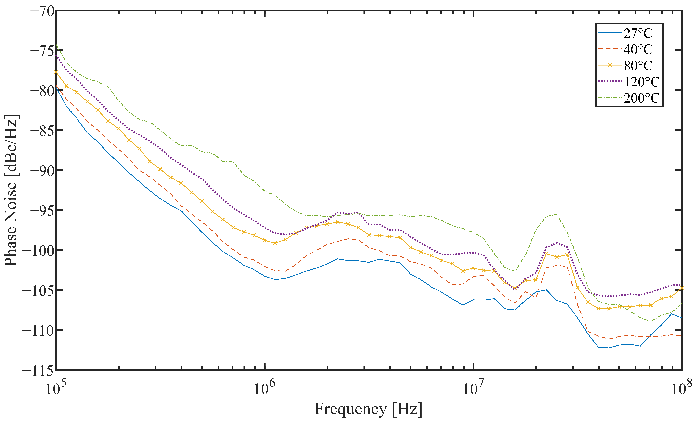
5.2. Thermal Characterization

The high-temperature thermal characterization was performed by locally raising the temperature around the fabricated chip with a temperature-controlled system, avoiding the unwanted effects generated by commercial-off-the-shelf (COTS) devices, used for the biasing of the test chip, when exposed to a high temperature [21]. Measuring the oscillation frequency for different frequency points from 27 °C to 200 °C, a frequency shift of the central frequency in the range between −3.34% and −5.72% is observed, as highlighted in Figure 12.
A decrease in frequency was expected since, as shown in Section 2, the frequency depends mainly on the output resistance of each stage and the input capacitance of the next stage. While the latter does not strongly depend on temperature, the value of the output resistor increases with increasing temperature. In fact, its value is mainly composed of the pull-up resistor value of the CML stage, which is designed using n-type poly resistors with a positive temperature dependency. However, the temperature dependency of the proposed RO-VCO is limited as compared to inverter-CMOS-based RO-VCOs. Indeed, the key elements that cause a frequency shift in inverter-CMOS-based systems, such as the carrier mobility and MOSFET threshold voltage, have a reduced impact on the proposed solution’s oscillation frequency.
An increment in the oscillator phase noise was also measured when the RO-VCO was exposed to a high temperature. In particular, at 1 MHz from the carrier, a phase noise increment of about 10.3 dB at 200 °C was observed, as shown in Figure 13.

6. State-of-the-Art Comparison

In this section, the RO-VCOs found in the literature and market are compared with the RO-VCO proposed in this paper. In order to extend the comparison, designs on different technology nodes were considered, such as 180 nm, 130 nm, and 65 nm. A summary of the compared RO-VCO is reported in Table 2. In [22], a very low-power 5.4 GHz fully differential RO-VCO with a tuning range from 4.9 to 5.9 GHz is proposed. The oscillator was implemented with active inductors to improve its bandwidth and used a three-stage differential output buffer to increase its driving ability. A comparison with its silicon area is not possible because only schematic simulations are presented. In [23], the improved performance of the RO-VCO based on single-ended differential pair configuration is presented. The high-frequency analysis revealed that the single-ended output delay stage provides better frequency stability than the differential output delay stage. Compared to the other works, the proposed approach occupies the least amount of space. A RO-VCO based on single-ended stages was presented in the cumulative work [24,25]. Its frequency ranges from 2.26 to 3.50 GHz, and its schematic simulations show a very low power consumption. However, no area occupancy nor experimental measurements are presented. In [26], a 7 GHz RO-VCO in 130 nm was presented. It is composed of three symmetrical stages connected together employing a multiloop technique for frequency boosting. It was measured by the use of an additional buffer for pads and probe driving. The driver is responsible for about one-third of the whole power consumption reaching 60 mW. Concerning the ring oscillator designed in 65 nm technology, in [27], a clock multiplier based on a ring oscillator is presented. It is able to cover a frequency range from 2.5 to 5.75 GHz with lower power consumption, but a nine times an area overhead of the proposed solution. In [28], a low-power VCO for Bluetooth front-end receiver in Internet of Things applications is presented. Thanks to its variable gain, it is able to cover a large frequency range with a low power consumption and silicon area, but with about a 30 dBc greater phase noise compared with the proposed RO-VCO. For pad driving purposes, an additional buffer capable of converting the differential signals provided by the RO-VCO to a single-ended signal is added to the output. In [29], a five-stage ring oscillator based on CML cells is proposed. It covers a wide tuning range by adopting two control techniques: variable capacitors using voltage-controlled varactors and supply voltage variation using a low dropout regulator. However, compared to the proposed solution, the simulation results reveal nearly double the power consumption and 24.9 dBc greater phase noise. A much wider tuning range from 2.4 to 11 GHz was achieved in the device proposed in [30], which employs three ring oscillators, which were properly selected to cover the entire range. Each RO-VCO was implemented using CML stages with negative resistance. The achievement of a such wide tuning range comes at the expense of more power consumption and lower phase noise performance when compared to the proposed RO-VCO. Since it uses three RO-VCOs, compared to the other solutions a greater area is expected even if its value is not reported. An even extended tuning range from 4.25 to 21.31 GHz is shown in [31]. It presents the simulation results of a four-stage RO-VCO with double feedback and two control voltages. The first acts on the speed of the delay cells’ internal feedback and the second changes the supply voltage of the delay cells. When compared with the proposed RO-VCO, the wide tuning range is paid for with more than double the power consumption and a 12.73 dBc greater phase noise simulated at the lowest frequency (4.25 GHz).
The Figure of Merit (FoM) measured at 1 MHz from the carrier that is provided in Equation (6) was utilized to account for the many factors defining the RO-VCO.
F o M = P N Δ f 20 l o g f 0 Δ f + 10 l o g P D C 1 mW · a r e a 1 mm 2
where P N Δ f is the VCO phase noise evaluated at Δ f from the target frequency f 0 and P D C is the power consumption of the controlled oscillator.
To summarize, the state-of-the-art comparison highlighted that the proposed tapered RO-VCO design achieved good phase noise and FoM values compared to other architectures. In addition, the proposed RO-VCO was experimentally demonstrated to operate properly up to 200 °C, yet maintaining good performances. The silicon area and power consumption of the proposed RO-VCO may appear not particularly good at first glance; however, this is primarily due to the direct integration of the output driver within the RO-VCO. To boost their driving strength, the other solutions require an extra output driver, which increases the power consumption and silicon area.

7. Conclusions

In this paper, the full-custom design of an asymmetric three-stage RO-VCO based on commercial 65 nm CMOS technology was presented together with the electrical and thermal characterization.
The analysis of a generic RO-VCO showed that raising the tapering factor K and the capacitor load, while accounting for the capacitance ratio α , can result in a reduction in area and power consumption. However, this achievement has to be paid for with a greater ω 0 , which depends on the technology and on the required voltage swing. However, because advanced technologies permit large ω 0 and the computing unit’s working frequency can be limited to a few GHz, rather than ballasting the RO-VCO with more capacitance or increasing the size of each stage in a symmetric way, the K and α factors can be increased. This not only allows the desired frequency to be achieved, but also improves the RO-VCO’s drive capability. In this perspective, instead of designing the classic RO-VCO with K = 1 and α = 1 , in this paper, the design of an asymmetric RO-VCO with K = 2 and α = 18.8 is proposed. The solutions used in the schematic design were described in detail, including the sizing of each device in the CML cells used to accomplish the 5.5 GHz target frequency. Furthermore, the design methodologies employed throughout the layout phase were discussed, with an emphasis on high-frequency and high-temperature concerns.
The experimental measurements of the proposed RO-VCO showed a tuning range from 4.72 GHz to 6.12 GHz and a cycle-to-cycle jitter with a mean value of 0.08 ps and a standard deviation of about 2.11 ps. Targeting applications where high-temperature operation conditions can occur, the fabricated RO-VCO was exposed to high temperatures up to 200 °C, and its performance variation was measured. In particular, at 200 °C, a decrement of the central oscillation frequency was registered in the range between −3.34% and −5.72%, while a phase noise increment of 10 dB at 1 MHz from the carrier was measured. Considering the comparison between the performance of the proposed RO-VCO and that present in the state-of-the-art, the proposed solution achieved good phase noise and FoM values, even if the area and power consumption were penalized because the out buffer was already integrated in the RO-VCO.

Author Contributions

G.C.: investigation, methodology, conceptualization, software, writing—review, and editing; D.M.: investigation, methodology, conceptualization, writing—review, and editing; M.M.: writing—review and editing; D.R.: writing—review and editing; S.S.: writing—review and editing. All authors contributed to the present paper with the same effort in finding available literature resources, as well as writing the paper. All authors have read and agreed to the published version of the manuscript.

Funding

This research received no external funding.

Data Availability Statement

Not applicable.

Acknowledgments

The authors would like to thank the RFLab of the Department of Information Engineering of the University of Pisa for their technical support and useful discussion. Work partially supported by the Italian Ministry of Education and Research (MIUR) in the framework of the CROSSLab and FoReLab projects (Departments of Excellence).

Conflicts of Interest

The authors declare no conflict of interest.

References

  1. Dubitzky, W.; Kurowski, K.; Schott, B. Large-Scale Computing Techniques for Complex System Simulations; John Wiley & Sons: Hoboken, NJ, USA, 2012. [Google Scholar]
  2. Buchty, R.; Heuveline, V.; Karl, W.; Weiss, J.-P. A survey on hardware-aware and heterogeneous computing on multicore processors and accelerators. Concurr. Comput. Pract. Exp. 2012, 24, 663–675. [Google Scholar] [CrossRef]
  3. Karimi, N.; Kong, Z.; Chakrabarty, K.; Gupta, P.; Patil, S. Testing of Clock-Domain Crossing Faults in Multi-core System-on-Chip. In Proceedings of the 2011 Asian Test Symposium, New Delhi, India, 20–23 November 2011; pp. 7–14. [Google Scholar]
  4. Adetomi, A.; Enemali, G.; Arslan, T. Clock buffers, nets, and trees for on-chip communication: A novel network access technique in FPGAs. In Proceedings of the 2017 IEEE International Parallel and Distributed Processing Symposium Workshops, Lake Buena Vista, FL, USA, 29 May 2017–2 June 2017; pp. 219–222. [Google Scholar]
  5. Restle, P.J.; McNamara, T.G.; Webber, D.A.; Camporese, P.J.; Eng, K.F.; Jenkins, K.A.; Allen, D.H.; Rohn, M.J.; Quaranta, M.P.; Boerstler, D.W.; et al. A clock distribution network for microprocessors. In Proceedings of the IEEE JSSC, Honolulu, HI, USA, 15–17 June 2000; Volume 36, pp. 792–799. [Google Scholar]
  6. Deutsch, A.; Kopcsay, G.V.; Restle, P.J.; Smith, H.H.; Katopis, G.; Becker, W.D.; Coteus, P.W.; Surovic, C.W.; Rubin, B.J.; Dunne, R.P.; et al. When are transmission-line effects important for on-chip interconnections? IEEE Trans. Microw. Theory Tech. 1997, 45, 1836–1846. [Google Scholar]
  7. Farshidi, A.; Behjat, L.; Rakai, L. David Westwick A Multiobjective Cooptimization of Buffer and Wire Sizes in High-Performance Clock Trees. IEEE Trans. Circuits Syst. II Express Briefs 2017, 64, 412–416. [Google Scholar]
  8. Mestice, M.; Neri, B.; Ciarpi, G.; Saponara, S. Analysis and Design of Integrated Blocks for a 6.25 GHz Spacefibre PLL. Sensors 2020, 20, 4013. [Google Scholar] [CrossRef]
  9. Li, P.; Tian, T.; Wu, B.; Ye, T. A Novel Self-Biased Phase-Locked Loop Scheme for WLAN Applications. Electronics 2021, 10, 2077. [Google Scholar]
  10. Danilo, M.; Gabriele, C.; Sergio, S. Design and Verification of a 6.25 GHz LC-Tank VCO integrated in 65 nm CMOS Technology Operating 340 up to 1 Grad TID. IEEE Trans. Nucl. Sci. 2021, 68, 2524–2532. [Google Scholar]
  11. Ciarpi, G.; Puccioni, G.; Mestice, M.; Monda, D.; Rossi, D.; Saponara, S. A 2 GHz Wide Tuning Range LC-Tank Digitally Controlled Oscillator in 28 nm CMOS Technology. In Applications in Electronics Pervading Industry, Environment and Society: APPLEPIES; Springer International Publishing: Cham, Switzerland, 2023; in press. [Google Scholar]
  12. Monda, D.; Ciarpi, G.; Saponara, S. Analysis and Comparison of Rad-Hard Ring and LC-Tank Controlled Oscillators in 65 nm for SpaceFibre Applications. Sensors 2020, 20, 4612. [Google Scholar] [CrossRef]
  13. Mestice, M.; Biondi, G.; Ciarpi, G.; Rossi, D.; Saponara, S. A Low-Area, Low-Power, Wide Tuning Range Digitally Controlled Oscillator for Power Management Systems in 28 nm CMOS technology. In Applications in Electronics Pervading Industry, Environment and Society: APPLEPIES; Springer International Publishing: Cham, Switzerland, 2023; in press. [Google Scholar]
  14. Farahabadi, P.M.; Miar-Naimi, H.; Ebrahimzadeh, A. Closed-form analytical equations for amplitude and frequency of high-frequency CMOS ring oscillators. IEEE Trans. Circuits Syst. I Regul. Pap. 2009, 56, 2669–2677. [Google Scholar] [CrossRef]
  15. Voinigescu, S. High-Frequency Integrated Circuits; Cambridge University Press: Cambridge, UK, 2013. [Google Scholar]
  16. Monda, D.; Ciarpi, G.; Saponara, S. Analysis and Comparison of Ring and LC-tank Oscillators for 65 nm Integration of Rad-Hard VCO for SpaceFibre Applications. Sensors 2020, 627, 25–32. [Google Scholar]
  17. Jin, J.; Jin, Y.; Gan, Y. A 500 kHz to 150 MHz Multi-Output Clock Generator Using Analog PLL and Open-Loop Fractional Divider with 0.13 µm CMOS. Electronics 2022, 11, 2347. [Google Scholar]
  18. Chen, Q.; Shan, Q.; Wei, Z.; Wang, X.; Huang, S.; Liu, Y. A Low-Power ADPLL with Calibration-Free RO-Based Injection-Locking TDC for BLE Applications. Electronics 2022, 11, 1953. [Google Scholar] [CrossRef]
  19. Alvero-Gonzalez, L.M.; Medina, V.; Kampus, V.; Paton, S.; Hernandez, L.; Gutierrez, E. Ring-Oscillator with Multiple Transconductors for Linear Analog-to-Digital Conversion. Electronics 2021, 10, 1408. [Google Scholar] [CrossRef]
  20. Heydari, P. Design and analysis of low-voltage current-mode logic buffers. In Proceedings of the Fourth International Symposium on Quality Electronic Design, San Jose, CA, USA, 24–26 March 2003; pp. 293–298. [Google Scholar]
  21. Saponara, S.; Ciarpi, G. Electrical, Electromagnetic, and Thermal Measurements of 2-D and 3-D Integrated DC/DC Converters. IEEE Trans. Instrum. Meas. 2018, 67, 1078–1090. [Google Scholar] [CrossRef]
  22. Zhang, C.; Li, Z.; Fang, J.; Zhao, J.; Guo, Y.; Chen, J. A novel high-speed CMOS fully-differential ring VCO. In Proceedings of the 12th IEEE International Conference on Solid-State and Integrated Circuit Technology, Guilin, China, 28–31 October 2014; pp. 1372–1375. [Google Scholar]
  23. Goyal, B.; Suman, S.; Ghosh, P.K. Design and analysis of improved performance ring VCO based on differential pair configuration. In Proceedings of the International Conference on Electrical, Electronics, and Optimization Techniques (ICEEOT), Chennai, India, 3–5 March 2016; pp. 3468–3472. [Google Scholar]
  24. Kinger, B.; Suman, S.; Sharma, K.G.; Ghosh, P.K. Design of Improved Performance Voltage Controlled Ring Oscillator. In Proceedings of the Fifth International Conference on Advanced Computing & Communication Technologies, Haryana, India, 21–22 February 2015; pp. 441–445. [Google Scholar]
  25. Suman, S.; Sharma, K.G.; Ghosh, P.K. Design of PLL using improved performance ring VCO. In Proceedings of the International Conference on Electrical, Electronics, and Optimization Techniques (ICEEOT), Chennai, India, 3–5 March 2016; pp. 3478–3483. [Google Scholar]
  26. Liu, H.Q.; Goh, W.L.; Siek, L.; Lim, W.M.; Zhang, Y.P. A Low-Noise Multi-GHz CMOS Multiloop Ring Oscillator with Coarse and Fine Frequency Tuning. IEEE Trans. Very Large Scale Integr. (VLSI) Syst. 2009, 17, 571–577. [Google Scholar]
  27. Coombs, D.; Elkholy, A.; Nandwana, R.K.; Elmallah, A.; Hanumolu, P.K. A 2.5-to-5.75 GHz 5 mW 0.3 psrms-jitter cascaded ring-based digital injection-locked clock multiplier in 65 nm CMOS. In Proceedings of the 2017 IEEE ISSCC, San Francisco, CA, USA, 5–9 February 2017; pp. 152–153. [Google Scholar]
  28. Yen, C.; Nasrollahpour, M.; Hamedi-Hagh, S. Low-power and high-frequency ring oscillator design in 65 nm CMOS technology. In Proceedings of the IEEE 12th International Conference on ASIC (ASICON), Guiyang, China, 25–28 October 2017; pp. 533–536. [Google Scholar]
  29. Samaras, D.; Tsimpos, A.; Hatzopoulos, A. A novel wide frequency range 65 nm CMOS VCO. In Proceedings of the 2022 IFIP/IEEE 30th International Conference on Very Large Scale Integration (VLSI-SoC), Patras, Greece, 3–5 October 2022; pp. 1–4. [Google Scholar]
  30. Samaras, D.; Hatzopoulos, A. High performance, wide tuning range 65 nm CMOS tunable Voltage Controlled Ring Oscillator up to 11 GHz. In Proceedings of the 2020 9th International Conference on Modern Circuits and Systems Technologies (MOCAST), Bremen, Germany, 7–9 September 2020; pp. 1–4. [Google Scholar]
  31. Askari, S.; Saneei, M.; Salem, S. Design and Analysis of Wide Tuning Range Ring VCO in 65 nm CMOS Technology. Radioelectron. Commun. Syst. 2019, 62, 232–240. [Google Scholar]
Figure 1. Model of a generic controlled oscillator based on asymmetric cells with a tapered factor K. The figure represents an RO-VCO with three cells, but it can be extended to a generic number of cells.
Electronics 12 00778 g001
Figure 2. Graphical representation of the area and power ratio reported in Equations (4) and (5) as a function of K and α .
Electronics 12 00778 g002
Figure 3. Electric schematic of the 3-stage differential and asymmetrical RO-VCO with the simple current mirror.
Electronics 12 00778 g003
Figure 4. Electric schematic of the generic xth stage based on the CML buffer with the addition of a varactor couple for frequency tuning.
Electronics 12 00778 g004
Figure 5. Whole schematic of the proposed three-stage RO-VCO.
Electronics 12 00778 g005
Figure 6. Layout of the proposed controlled oscillator.
Electronics 12 00778 g006
Figure 7. On the left, a photo of the high-speed board used for testing purposes. On the right, a microscope photo of the bare chip directly bonded with aluminum bonding wires on the high-frequency test board.
Electronics 12 00778 g007
Figure 8. Image of the RO-VCO output signal spectrum performed with the Spectrum Analyzer. The spectrum is centered on the VCO central frequency.
Electronics 12 00778 g008
Figure 9. Measurement results of the proposed RO-VCO as a function of the control voltage: the black solid curve shows the free-running frequency, and the blue dotted curve represents the oscillator gain.
Electronics 12 00778 g009
Figure 10. Image of the RO-VCO output signal measured with the oscilloscope: the black solid and the blue dotted traces were measured for the minimum and maximum RO-VCO control voltages, respectively. Both traces are triggered in the center of the graphic.
Electronics 12 00778 g010
Figure 11. The cycle-to-cycle jitter histogram, measured with a 23 GHz 100 GS/s Tektronix mixed-signal oscilloscope evaluated at the target frequency of the RO-VCO.
Electronics 12 00778 g011
Figure 12. Central frequency variation for different control voltages as a function of the temperature between 27 °C and 200 °C.
Electronics 12 00778 g012
Figure 13. Phase noise measurements as a function of temperature between 27 °C and 200 °C. Around 2.5 MHz and 25 MHz from the carrier, an anomalous peak is observed, probably due to the COTS on the testing board used for the generation of the power supply and bias.
Electronics 12 00778 g013
Table 1. VCO components size.
NameWLValues
M 1 24 µm60 nm-
R D 1 --640 Ω
M 2 48 µm60 nm-
R D 2 --320 Ω
M 3 96 µm60 nm-
R D 3 --160 Ω
C L --350 fF
M b 0 89.6 µm240 nm-
M b 1 89.6 µm240 nm-
M b 2 179.2 µm240 nm-
M b 3 358.4 µm240 nm-
Table 2. State-of-the-art comparison table.
Ref.[22][23][24,25][26][27]
Technology (nm)18018013013065
Frequency Range (GHz)4.9–5.95.3–6.62.2–3.57.30–7.862.5–5.75
Silicon Area (mm2)n.a.3.18 × 10 5 n.a.1.6 × 10 2 9.0 × 10 2
Power Consumption (mW)8.12.9–6.80.031–0.052605.3
Extra Output Buffer Neededyesyesyesyesyes
Phase Noise @ 1 MHz (dBc/Hz)−86.7n.a.n.a.−103.4−113
Maximum Temperature (°C)n.a.n.a.n.a.n.a.n.a.
Data TypeSimul.Simul.Simul.Meas.Meas.
FoM @ 1 MHz (dBc/Hz)n.a.n.a.n.a.−181−185.5
Ref.[28][29][30][31]This work
Technology (nm)6565656565
Frequency Range (GHz)3.7–6.52.75–5.72.4–114.25–21.314.7–6.1
Silicon Area (mm2)1.10 × 10⁻²n.a.n.a5.4 × 10 4 1.00 × 10 2
Power Consumption (mW)2.3292033.1315.45
Extra Output Buffer Neededyesyesyesyesintegrated
Phase Noise @ 1 MHz (dBc/Hz)−71.0−78.13−90.08−90.47−103.2
Maximum Temperature (°C)n.a.125n.a.75200
Data TypeSimul.Simul.Simul.Simul.Meas.
FoM @ 1 MHz (dBc/Hz)−161.8n.an.a.−180.5−186
Disclaimer/Publisher’s Note: The statements, opinions and data contained in all publications are solely those of the individual author(s) and contributor(s) and not of MDPI and/or the editor(s). MDPI and/or the editor(s) disclaim responsibility for any injury to people or property resulting from any ideas, methods, instructions or products referred to in the content.

