
Uniform Linear Antenna Array Beamsteering Based on Phase-Locked Loops

Abstract
:1. Introduction
2. Antenna Basics
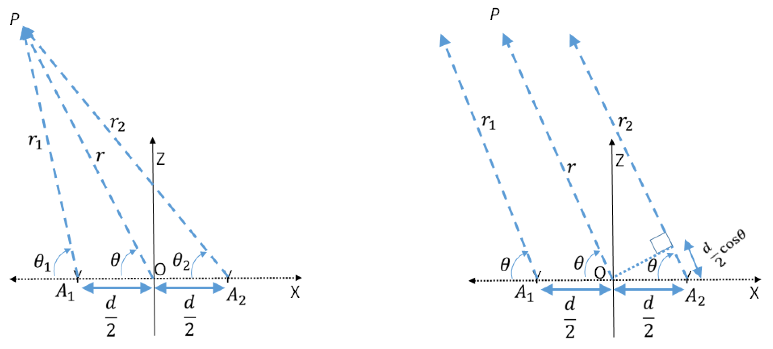
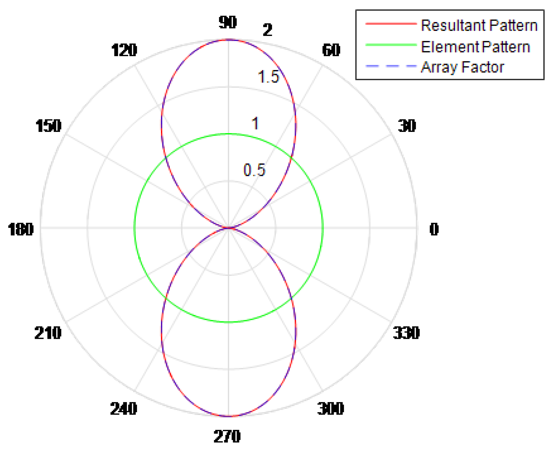
2.1. Array Theory
2.2. Uniform Linear Array with N Elements
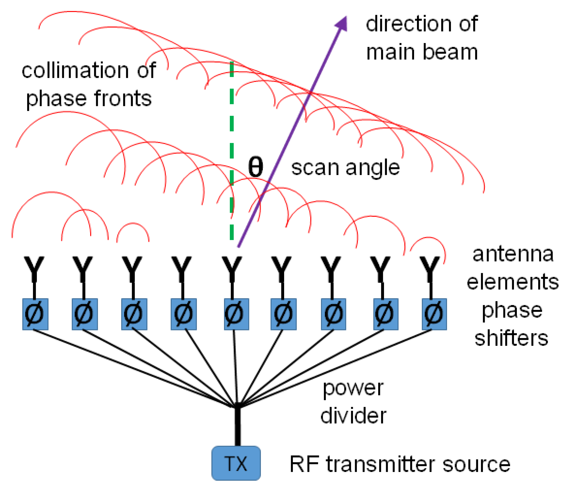
2.3. Beam Steering
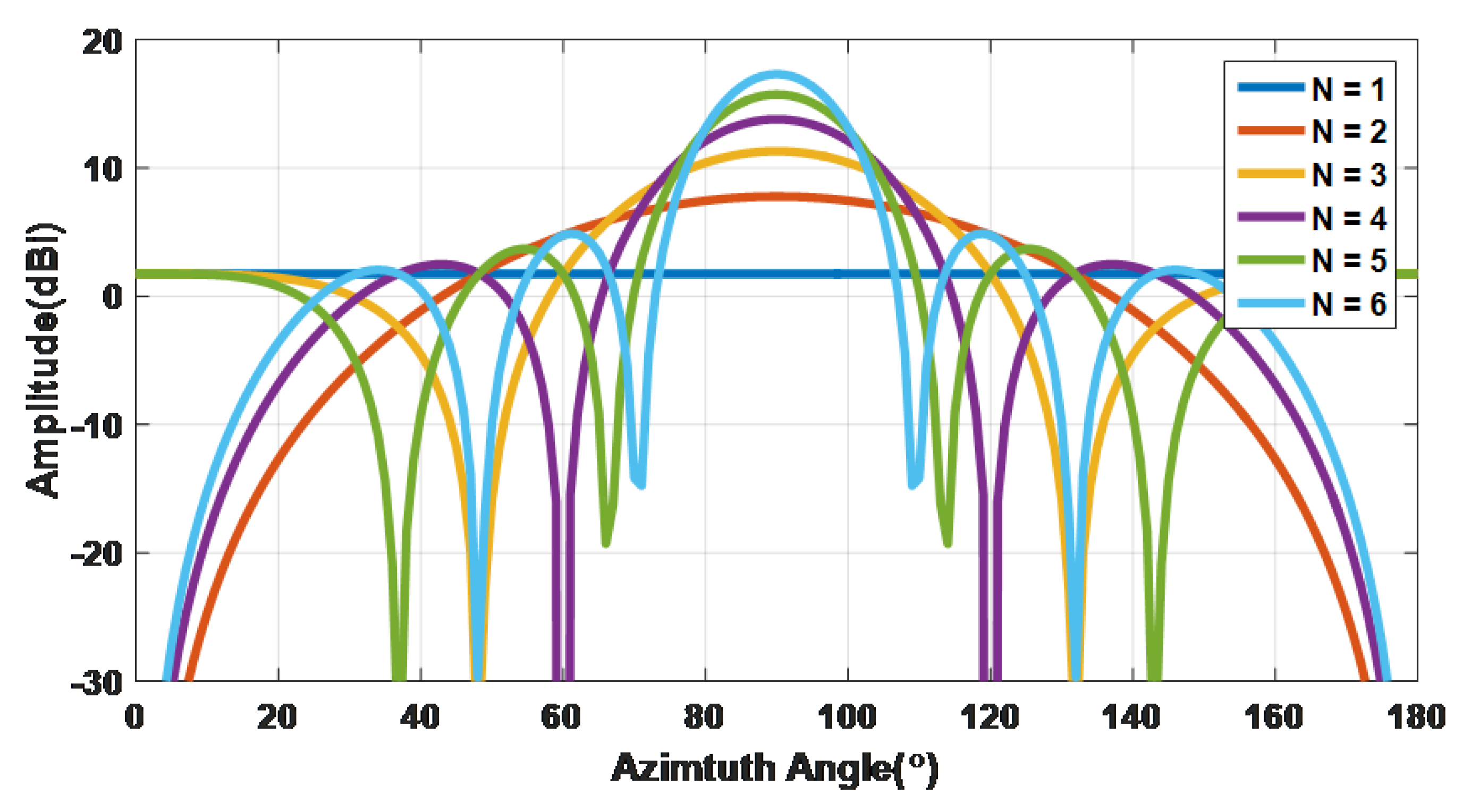
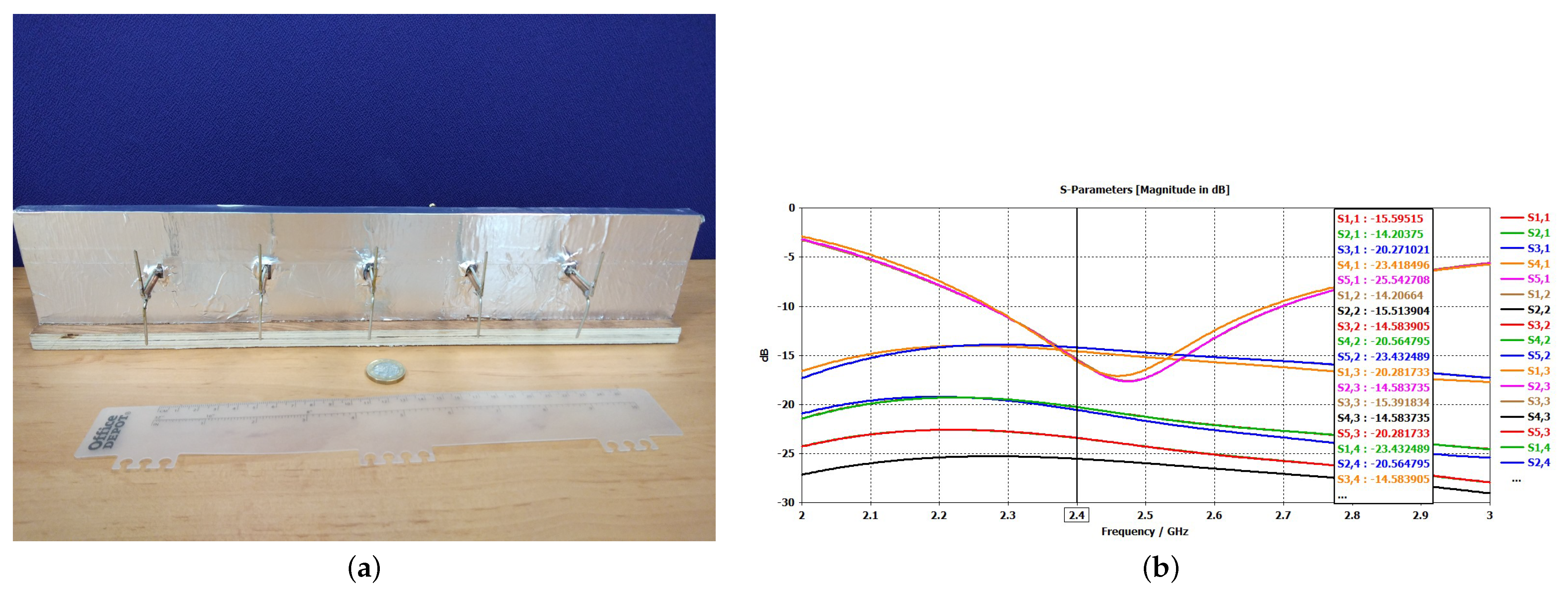
3. N-Element Array Design
Defining Array Parameters
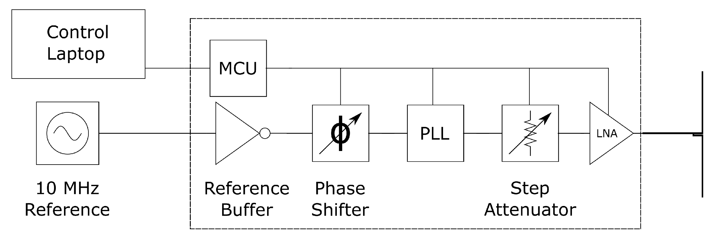
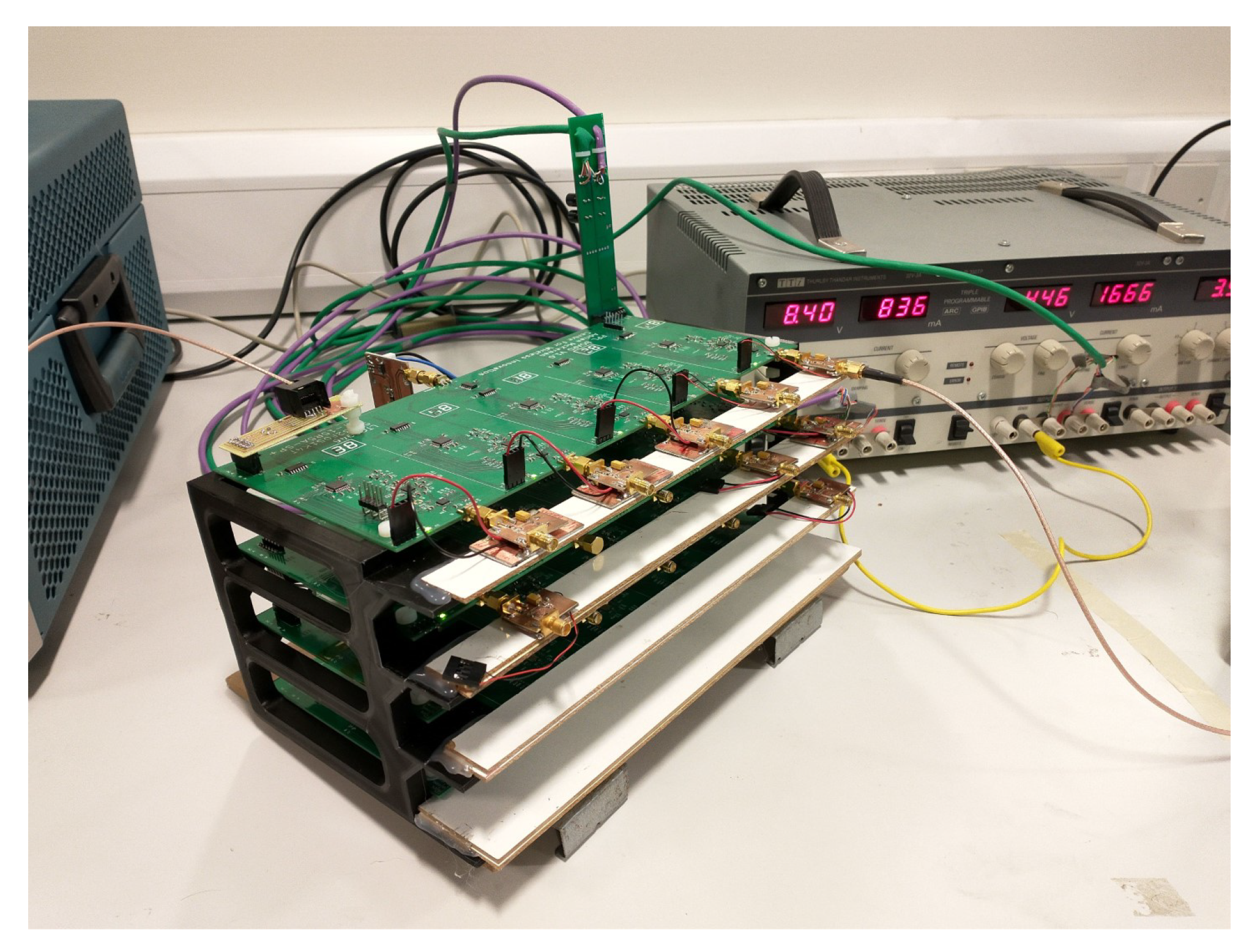
4. Hardware Required
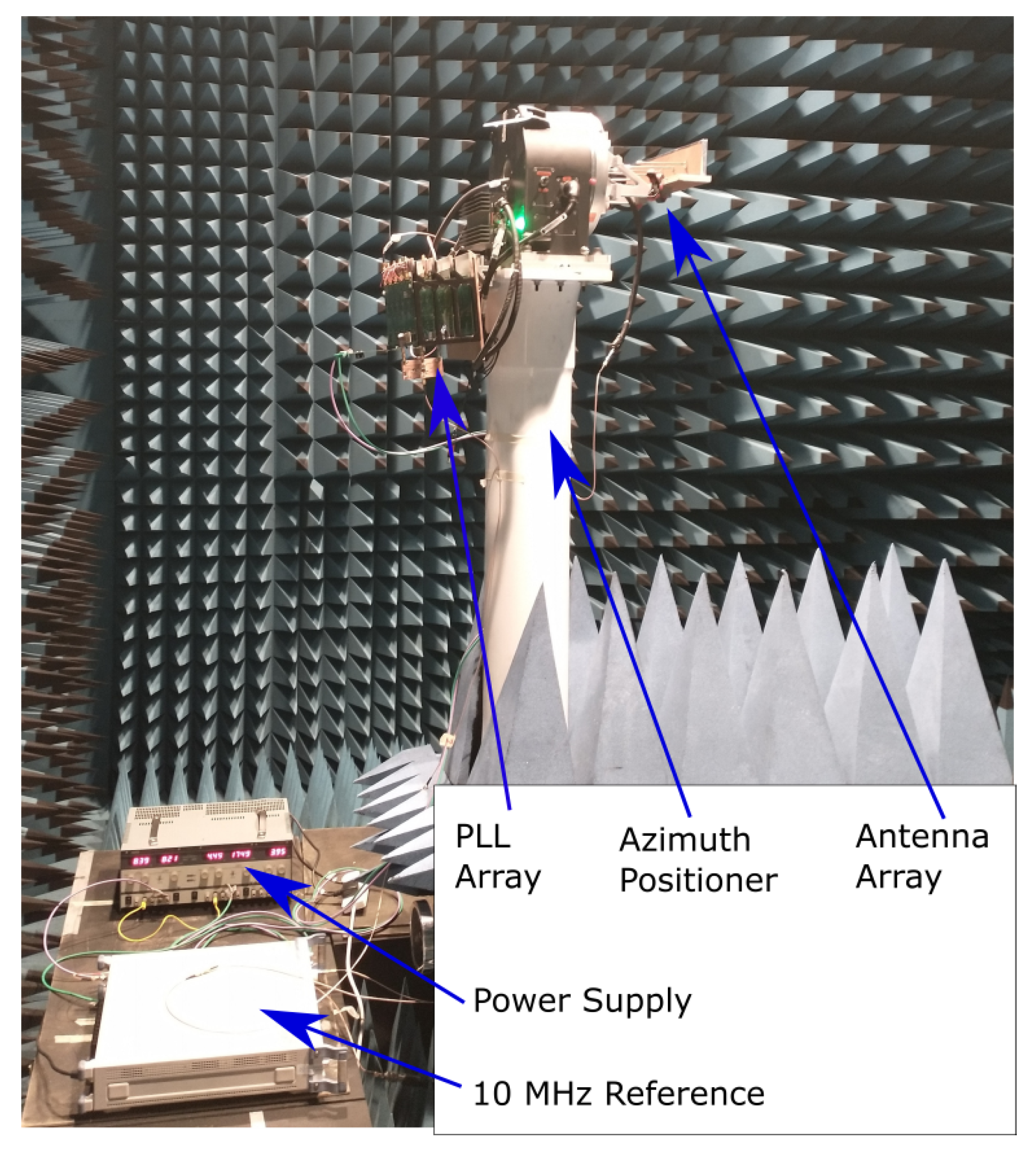
5. Measurement on ULA
Calibration Process and Pattern Measurement
6. Conclusions
Author Contributions
Funding
Data Availability Statement
Acknowledgments
Conflicts of Interest
References
- Blaunstein, N.; Christodoulou, C.G. Antenna Fundamentals; Wiley: Hoboken, NJ, USA, 2014; Available online: https://ieeexplore.ieee.org/document/8042843 (accessed on 31 January 2023).
- Balanis, C.A. Fundamental Parameters and Definitions for Antennas; Wiley: Hoboken, NJ, USA, 2008. [Google Scholar] [CrossRef]
- Haupt, R.L. Timed and Phased Array Antennas; IEEE: Piscataway, NJ, USA, 2015. [Google Scholar] [CrossRef]
- Hansen, R.C. Linear Array Pattern Synthesis; Wiley: Hoboken, NJ, USA, 2010. [Google Scholar] [CrossRef]
- Mailloux, R.J. Electronically Scanned Arrays; Springer Cham: Manhattan, NY, USA, 2007. [Google Scholar] [CrossRef]
- PLL Array Production Files and Software. 2022. Available online: https://adrian-mckernan.github.io/ (accessed on 31 January 2023).
- Haupt, R.L. Array Beamforming; Wiley-IEEE Press: Hoboken, NJ, USA, 2015. [Google Scholar] [CrossRef]
- MATLAB, Matrix Laboratory. [Online]. Available online: http://www.mathworks.com (accessed on 31 January 2023).
- James, J.; Hall, P.; Wood, C. Microstrip Antenna: Theory and Design; Ser. IEE Electrical Measurement Series; Peregrinus: London, UK, 1986. [Google Scholar] [CrossRef]
- LTC6946 Low Noise Integer-N PLL with Integrated VCO, Analog Devices, 03. 2015. [Online]. Available online: https://www.analog.com/en/products/ltc6946.html (accessed on 31 January 2023).
- SNx4HC04 Hex Inverters Datasheet (Rev. G), Texas Instruments, 09 2015, rev. G. [Online]. Available online: https://www.ti.com/product/SN74HC04 (accessed on 31 January 2023).
- BB202 Low-Voltage Variable Capacitance Diode, NXP Semiconductors, 01 2008, rev. 02. [Online]. Available online: https://www.nxp.com/docs/en/data-sheet/BB202_N.pdf (accessed on 31 January 2023).
- Digital Step Attenuator, Mini Circuits, 01 2005, rev. C. [Online]. Available online: https://www.minicircuits.com/pdfs/DAT-15R5A-SP+.pdf (accessed on 31 January 2023).
- MAX2692/MAX2695 WLAN/WiMAX Low-Noise Amplifiers, Maxim, 09 2011. [Online]. Available online: https://datasheets.maximintegrated.com/en/ds/MAX2692-MAX2695.pdf (accessed on 31 January 2023).
- RM0091 Reference Manual STM32F0x1/STM32F0x2/STM32F0x8, STM Microelectronics, 01 2017. [Online]. Available online: https://www.st.com/en/microcontrollers-microprocessors/stm32f0-series.html (accessed on 31 January 2023).
- Hansen, R.C. Measurements and Tolerances; Wiley: Hoboken, NJ, USA, 2010. [Google Scholar] [CrossRef]


| Parameter | Desired Range | Value Single Element |
|---|---|---|
| Frequency (GHz) | 2.4 | 2.4 |
| Return loss (dB) | 10 | 10 |
| Gain (dB) | 10 | 2.1 |
| 3 dB beamwidth (°) | 21 | Omni-directional |
| 10 dB bandwidth (MHz) | 100 | 100 |
| Scan Angle () | Progressive Phase () |
|---|---|
| 0 | −180 |
| 30 | −155.9 |
| 45 | −127.3 |
| 60 | −90 |
| 90 | 0 |
| 120 | 90 |
| 135 | 127.3 |
Disclaimer/Publisher’s Note: The statements, opinions and data contained in all publications are solely those of the individual author(s) and contributor(s) and not of MDPI and/or the editor(s). MDPI and/or the editor(s) disclaim responsibility for any injury to people or property resulting from any ideas, methods, instructions or products referred to in the content. |
© 2023 by the authors. Licensee MDPI, Basel, Switzerland. This article is an open access article distributed under the terms and conditions of the Creative Commons Attribution (CC BY) license (https://creativecommons.org/licenses/by/4.0/).
Share and Cite
Chepala, A.; Fusco, V.; Naeem, U.; McKernan, A. Uniform Linear Antenna Array Beamsteering Based on Phase-Locked Loops. Electronics 2023, 12, 780. https://doi.org/10.3390/electronics12040780
Chepala A, Fusco V, Naeem U, McKernan A. Uniform Linear Antenna Array Beamsteering Based on Phase-Locked Loops. Electronics. 2023; 12(4):780. https://doi.org/10.3390/electronics12040780
Chicago/Turabian StyleChepala, Anil, Vincent Fusco, Umair Naeem, and Adrian McKernan. 2023. "Uniform Linear Antenna Array Beamsteering Based on Phase-Locked Loops" Electronics 12, no. 4: 780. https://doi.org/10.3390/electronics12040780