Abstract
This paper proposes a novel electrolytic-free quasi-Z-Source Ćuk LED driver for automotive applications. Compared to the traditional Ćuk converter, the first merit of the novel converter is higher gain, which makes it apt to switch between multiple applications. Secondly, the proposed converter combines the inherent characteristics of LED load to operate in a wide range in Continuous Conduction Mode (CCM), so the inductors can assist in energy storage, and only small capacitance is required. Thirdly, inductors can be integrated and use only one core, and capacitors are electrolytic-free, which will benefit integration and long life. All merits are important to automotive application. Detailed analysis and design steps are presented. Then, with the help of the simulation software Saber, several key parts of the converter are simulated. Finally, a prototype controlled by the micro control unit stm32f103c8t6 is built, and the feasibility is verified by the experiment results.
1. Introduction
LEDs are increasingly preferred in automotive lighting applications for their long lifetime, mechanical robustness, and energy saving [1,2]. Batteries (12/24 V) are commonly used as the input of LED drivers in automotive applications, and different battery voltage systems are available sometimes. Therefore, LED drivers capable of operating in a wide input range are needed [3,4,5]. In addition, different automotive applications, such as headlights, brake lights, and turn signals, require different levels of lighting brightness, so different numbers of LEDs in series are required. Moreover, the same application may require a different number of LEDs in series (such as headlamps for high beam and low beam).
Switched-mode dc–dc converters with both step-up and step-down capability can address the above challenges. A four-switch buck–boost converter [3] is presented, whose structure can be exchanged between the buck, boost, and buck–boost to provide a desired voltage gain, but the converter efficiency drops in the buck–boost operation due to the cascaded structure. Ćuk-converter-based automotive LED drivers have also been reported [6,7,8]. The Ćuk converter of [6] has reduced efficiency due to hard-switching at a 500 kHz switching frequency. High-frequency Ćuk converters that achieve zero-voltage switching are presented in [7,8], but they have two or more active switches to drive, with higher complexity and more components. The latest literature is mostly based on resonant converters [4,5,9,10,11,12,13]. These solutions have higher efficiency and a compact size, but similar to [7,8], they usually have more switches to drive and complex structure, and variable-frequency control usually necessitates the use of large EMI filters.
Life incompatibility between electrolytic capacitors and other components of LED drivers has gradually become one of the main concerns in recent years. There are two main solutions to this problem: through new topology or control schemes [14,15,16]. The authors of [17] used an inductor to assist energy storage, but the inductance is quite large because the inductor works at a low frequency.
Many new topologies have been proposed based on a quasi-Z-source network to achieve high-voltage gain [18,19,20,21]. Combining a quasi-Z-source network with the Ćuk converter, and integrating the three inductors, a novel high-gain quasi-Z-source Ćuk converter is proposed in this paper. It is suitable for a wide range of input and output, and requires small space. Because of the combination of characteristics with LED load, the converter works in CCM in a wide range, with small capacitance and long life.
This paper is organized as follows. Section 2 gives the circuit configuration and operating principle. Parameter design and control strategy are briefly described in Section 3. Then, in Section 4, the experimental results of a prototype are presented. Finally, the conclusions of this work are detailed in Section 5.
2. Circuit Configuration and Operating Principle
2.1. Circuit Configuration
The topology of the proposed quasi-Z-source Ćuk converter is shown in Figure 1 below, where Lz1, L1, L2 represent the three windings of the mutual inductors integrated on a magnetic core with the same number of turns. Compared with the traditional Ćuk converter, an inductor is replaced by the quasi-Z-source network, which is composed of L1, Lz1, capacitors Cz1, Cz2, and diode Dz1 surrounded by the sector dotted line. Dz2 is added to suppress the low-frequency oscillation between L1, Lz1, Cz1, Cz2 and input Vin under light load. The signs and arrows in Figure 1 indicate the positive direction of capacitor voltage and inductor current, respectively.
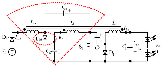
Figure 1.
Proposed quasi-Z-source Ćuk LED driver.
Figure 2 shows the equivalent circuit of the quasi-Z source Ćuk Converter in four work modes in steady state. The steady-state analysis of the integrated inductor in CCM can be firstly carried out as three independent inductors, as the inductor voltage and current change in the same direction, and the coupling of inductors only causes an increase in the equivalent inductance.
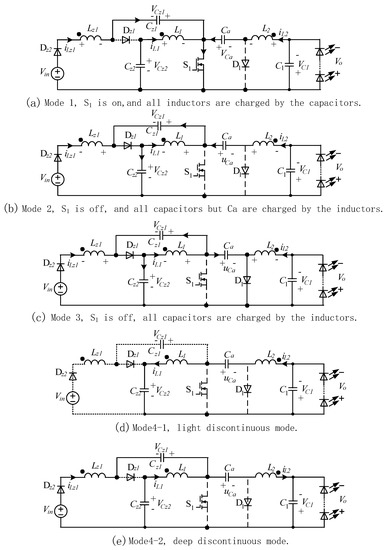
Figure 2.
Equivalent circuit of the proposed driver with four possible work modes.
The proposed converter contains three work modes as in Figure 2a–c in CCM, while it contains one more mode in Discontinuous Conduction Mode (DCM), which can be Figure 2d or Figure 2e according to the load. The arrows in Figure 2 indicate the actual direction of the loop current, and the positive and negative signs also indicate the actual direction of the element voltage. The work details are as follows:
Mode 1[t0–t1]: The switch S1 is turned on at t0, and Dz1 is reverse-biased for Vcz2 > Vcz1. D1 is also off by withstanding Vca. There are three current loops in this mode, and all the inductors are charged, while all the capacitors are discharging. The input voltage Vin and Cz1 are connected in series to charge Lz1; Cz2 charges L1, and Ca supplies power to L2 and the load.
Mode 2[t1–t2]: Mode 2 begins when S1 is turned off. It should be noted that except Ca, all the other inductors/capacitors interchange between storing and releasing energy in this mode. The operation of the converter can be divided into three parts. Vin and Lz1 are connected in series to charge Cz2, L1 charges Cz1, and Ca together with L2 supplies power to Cz1, Cz2, and the load.
Mode 3[t2–t3]: Ca also changes to be charged in this mode, and D1 is turned on. Therefore, all the inductors are discharging, while all the capacitors are charged. Part of iL1 and iLz1 are in series with Vin to charge Ca, and the remaining current of L1 and Lz1 is utilized to charge Cz1 and Cz2 separately. At the same time, L2 freewheels through D1 and charges the load.
Figure 3 presents the current and voltage waveforms on the integrated three inductors, and the current waveform of Ca, where ts is the switching cycle, and d1, d2, and d3 are the duty ratios corresponding to the duration of modes 1, 2, and 3, respectively. It is easy to understand that the voltage waveforms on the integrated three inductors are the same with the same number of turns, but the current waveforms of iL1 and iLz1 are different from iL2.
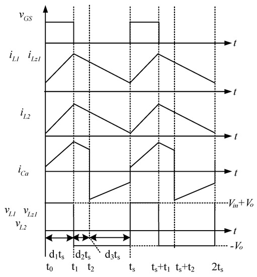
Figure 3.
Theoretical waveforms of the proposed converter in CCM.
If the load is light enough, the converter will enter into DCM, and the converter has a fourth mode in a switching cycle as in Figure 2d,e, where the switch and diodes are always off.
Mode 4-1[t3–ts]: iLz1 cannot be reversed due to Dz2 in light discontinuous mode, so it remains zero. The slew rate of iLz1 is zero, and the voltage on Lz1 is also zero, resulting in zero voltage on other windings of the mutual inductor at the same time. There is only one current loop: Ca charges C1 and Cz2, and iL1 and iL2 basically stay constant at this stage.
Mode 4-2[t3–ts]: Since the output current is very small and the output voltage is also higher in deep discontinuous mode, iL2 drops faster than iL1 and iLz1 to negative at the end of mode 3, while iL1 and iLz1 remain positive. The only thing that happens is that Cz1, Cz2, and C1 charge Ca with a constant current in this interval.
The theoretical waveforms of the proposed converter in DCM are presented in Figure 4 below. If the converter is just at the boundary of CCM and DCM, that is in Boundary Current Mode (BCM), iLz1 is zero at the end of the cycle. Note that there is no time that all winding currents are zero in this DCM, but the total magnetic flux of the core is zero during mode 4. Although the mutual inductor is designed to have the same name end when the voltage is applied, the reverse current always appears in DCM, which may actually reduce the equivalent inductance.
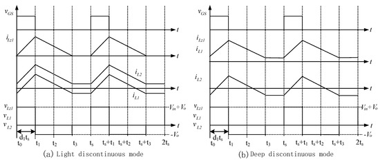
Figure 4.
Theoretical waveforms of the proposed converter in DCM.
The major feature is that the charging and discharging of the capacitors are always in series with the inductors, resulting in a smooth variation of the capacitor voltage. Therefore, the inductances and capacitances can be relatively small, which is good for integration and heat dissipation.
2.2. General Analysis
In the following analysis, the switch and diodes are assumed to be ideal. The voltage on Lz1, L1, L2 in CCM are given by Equations (1) and (2) below according to mode 1–3. Note that the equations of inductor voltage for mode 2 and 3 are the same:
Since the voltages on Lz1, L1, L2 are the same, the relationship between the capacitor voltages can be inferred from Equations (1) and (2):
Then the following relationship can be obtained from the volt-second balance of Lz1, L1, and L2:
Substituting Equation (3) into Equation (4), from the volt-second balance relationship of L1 and L2 we can get Vcz1 = Vo. Then, plugging it into the volt-second balance equation of Lz1 in Equation (4), and eliminating Vcz1 and Vcz2, yields the important relationship among input, output voltage, and duty ratio:
There is no mode 4 in CCM, so the relationship of duties becomes: d2 + d3 = 1 − d1. Substituting this into Equation (5), the expression for the output voltage in CCM is given by:
This relationship looks similar to the basic converters, where the output voltage is not directly related to the output current in CCM. Further analysis needs to introduce the current equation corresponding to the capacitor’s charge balance:
where α and β are the scale factors when iL1 and ilz1 are divided into two parts in mode 3, respectively. Since L1 and Lz1 charge Ca in series in mode 3, the current is equal, i.e.,
Regarding the circuit containing Dz1 enclosed by the dashed ellipse in Figure 1 as a node, Kirchhoff’s current law can be applied. Because of charge balance, the average current of Cz1 and Cz2 in a whole cycle is zero, so a new current relationship is achieved:
Synthesizing Equations (8) and (9), we know α = β. After substituting it back into Equation (7), we find that Cz1 and Cz2 are charged and discharged in the same way, and their charge balance equations are the same. According to mode 3, Cz1 and Cz2 are both charged by the current αIL1, and Ca is charged by the current (1 − α)IL1. The three capacitors form a voltage loop, so the voltage increment of these capacitors should be equal, that is:
Eliminate IL1 from Equation (10) and simplify the expression to obtain:
Thus, α is determined by the capacitance ratio. From Figure 2d or Figure 2e in mode 4, we know that:
Comparing Equations (12) and (3), we can infer that Vcz1 = Vo, and Vca = Vin + 2Vo.
The output voltage gain of the traditional Ćuk converter is d1/(1 − d1) in CCM. Figure 5 below shows the gain comparison between the traditional and the proposed Ćuk converter, whose gain is based on Equation (6). It can be seen that the output voltage of the quasi-Z-source converter is much larger than that of the traditional Ćuk converter in CCM.
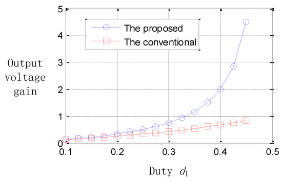
Figure 5.
Gain comparison between the traditional and the proposed Ćuk converter in CCM.
3. Parameter Design and Control Strategy
3.1. Boundary Analysis
The inductor can help to store energy only in CCM mode. Furthermore, the reverse flow of current occurs in DCM lead to lower efficiency. Therefore, the converter should be designed to operate in CCM, and the boundary current from CCM to the light DCM with a decrease in load current should be estimated, since iLz1 is zero at the end of the cycle in BCM, and the waveform of iLz1 in one cycle is triangular. According to the triangle area formula, the peak value is twice the average value. Therefore, it can be obtained from the analysis of mode 1 based on Faraday’s law of electromagnetic induction:
It is necessary to model the LED load to calculate the boundary load current. A single LED is modeled as a series connection of an ideal diode, a voltage source, and a resistor, similar as in [12]. The model circuit and its parameters used in the following analysis are shown in the Figure 6 below. The linearized model can be obtained by making a tangent at the rated current on the nonlinear voltage and current curve of power LED Luxeon LXM3-PW81 [22] used in the experiment, and the corresponding parameters can be achieved. Note that temperature factor is ignored here.
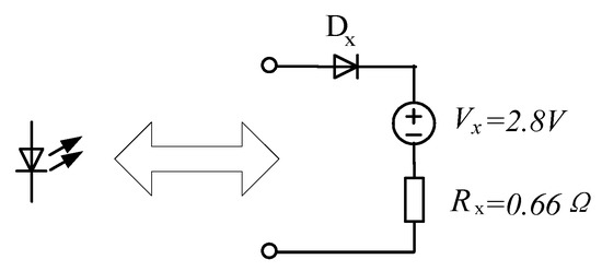
Figure 6.
Single LED model parameter.
According to this LED model, the output voltage can be obtained from Io:
where Nled represents the number of LEDs in the load.
Vo = Nled * Vx + Rx * Nled * Io
Given Vin, Lz1, and LED load, Io is initialized to be zero, Vo can be achieved through Equation (13). Three steps are taken to obtain the BCM load current, which is utilized to design the integrated inductor in the next subsection.
- d1 can be obtained from Equation (6), and the boundary current ILz1 can be inferred from Equation (13).
- From the balance of input and output power, we know that:
- 3.
- Then Io can be obtained.
- 4.
- A new Vo is calculated through Equation (14). The iteration stops when the error of Vo obtained by the two adjacent iterations is small enough, or we return to step 1.
When the error is set to 0.0001, less than 5 iterations are needed for a certain LED load.
3.2. Integrated Inductor Design
The design of the integrated inductor is decided by the CCM range of the load. The load current curve of BCM under different input voltages and different self-inductance of Lz1 is shown in Figure 7 based on the numerical iteration algorithm in the previous subsection. It can be seen that the boundary load current increases significantly with the increase in input voltage, and slightly increases with the decrease in the LED load. A self-inductance of 150 μH is selected to guarantee the converter to work in CCM in a wide range.
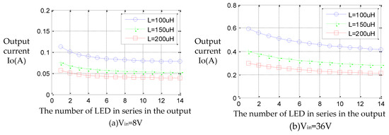
Figure 7.
Output boundary current in different input voltages with different self-inductance.
3.3. Circuit Control
Figure 8 shows the control block diagram of the proposed converter. To avoid excessive current during startup, soft startup is set in the program. At the beginning of startup, a slightly large duty is set for the converter for open-loop operation. The incremental current closed-loop PI duty cycle control is activated when the output current reaches within a certain range. Note that the output voltage of the proposed Ćuk converter is negative, so the potential of the sampling current on Rs is negative. A level-raising circuit is added to make it positive, and then the subsequent signal conditioning circuit and PI block are used to perform closed-loop control.
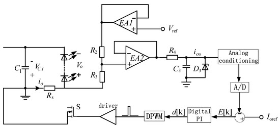
Figure 8.
Control block diagram of the proposed LED driver.
4. Simulation and Experimental Verification
The key of this converter simulation is the modeling of the multi-winding coupling inductor, which has been discussed in many studies recently [23,24]. Saber is a simulation software that can help. For the simulation model of mutual inductors, the coupling coefficient between windings should be defined in pairs, so three inductors and three coupling coefficients should be defined for three winding coupled inductors, as shown in Figure 9 below. In order to obtain a more accurate coupling coefficient, the windings of the fabricated coupling inductor are connected in series to measure mutual inductance in pairs. After obtaining the self-inductance of each winding, the simulation model is established.
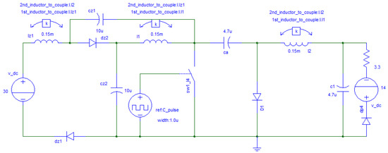
Figure 9.
Open-loop simulation circuit.
The simulation waveform in Figure 10 presents the operation waveforms of two DCM modes under different load current. In Figure 10a, iLz1 remains zero in the fourth mode, while iL1 is negative and iL2 is positive. In Figure 10b, both iLz1 and iL1 remain positive, while iL2 is negative for a period of time. The verification of the operation waveform of DCM mode provides the basis for the design of the integrated inductor, and also validates the theoretical analysis in the previous section.
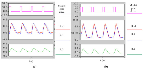
Figure 10.
Simulation waveforms of the DCM operation. (a) Light discontinuous operation waveform; (b) deep discontinuous operation waveform.
To verify the validity of the proposed LED driver, a prototype, shown in Figure 11, has been built and tested. The key components used in the prototype are listed in Table 1, and the control is realized by a micro control unit (stm32f103c8t6). The load consists of one LED string, according to the number of LEDs, and the output voltage ranges from 6 V to 36 V.
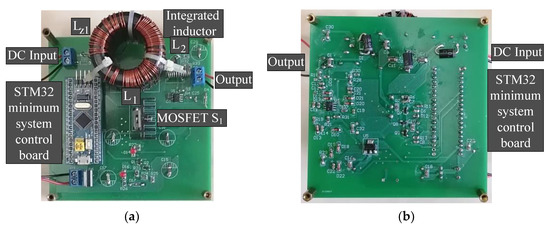
Figure 11.
Photograph of the prototype. (a) Front view; (b) back view.

Table 1.
Key parameters of the protype.
Figure 12 shows the startup waveform of Io, Vo, and Vca under a load of 2 LEDs and 12 LEDs in series with rated 0.5 A current, respectively. Before startup, Vca is equal to Vin; when S1 obtains the effective drive, Vca and Vo change immediately. Note that the output voltage is negative. It can be seen from the experimental waveform that the dynamic characteristics of the converter are relatively fast under different loads.
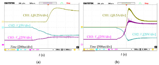
Figure 12.
Startup waveforms of Io, Vo, and Vca under different loads. (a) Output load with 2 LEDs in series; (b) output load with 12 LEDs in series.
Figure 13 displays the steady-state waveform of Io, Vo, and Vca under the load of 2 LEDs and 12 LEDs with rated 0.5 A current, respectively. It is indicated that the output is quite stable, and the output ripple current is less than 10% under the rated load.
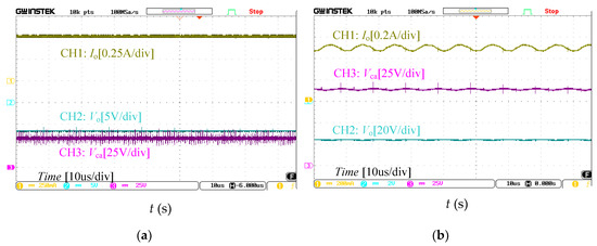
Figure 13.
Steady-state waveforms of Io, Vo, and Vca under different loads. (a) Output load with 2 LEDs in series; (b) output load with 12 LEDs in series.
Figure 14 shows the efficiency of the converter when the input voltage range is 8–36 V, where the corresponding number of load LEDs in series Nled is 2,6,10,12, and the rated output current is 0.5 A. It can be seen that the system efficiency increases gradually with the increase in input voltage and load. As the input voltage increases, the input current decreases, and the switch turn-off voltage rises. However, the decrease in the input current seems to have a greater impact on the efficiency.
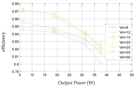
Figure 14.
Measured efficiency with input voltage ranging from 8 to 36 V under different LED loads.
5. Conclusions
In this paper, a novel quasi-Z-source Ćuk converter topology is proposed, and its work mode is analyzed in detail. Compared with the traditional Ćuk converter, its output voltage gain is greatly improved, which makes it more apt for wide input and load changes. Furthermore, the proposed converter combines the inherent characteristics of LED load to operate in a wide range in CCM, so the inductor can assist in energy storage, and electrolytic-free is available when small capacitance is required. In addition, inductors can be integrated and use only one core. Therefore, the converter requires less space. Finally, the feasibility of the proposed new topology is verified by experiments.
Author Contributions
Formal analysis, L.W.; Project administration, W.H.; Validation, W.H.; Writing—original draft, L.W.; Writing—review & editing, L.W. and W.H. All authors have read and agreed to the published version of the manuscript.
Funding
This research was funded by Hanshan Normal University, Dr. Scientific Research Fund, grant number QD20180126 and the Guangdong Basic and Applied Basic Research Foundation under grant 2021A1515010616.
Data Availability Statement
Not applicable.
Conflicts of Interest
The authors declare no conflict of interest.
References
- Pollock, A.; Pollock, H.; Pollock, C. High efficiency LED power supply. IEEE Trans. Emerg. Sel. Top. Power Electron. 2015, 3, 617–623. [Google Scholar] [CrossRef]
- Gacio, D.; Cardesin, J.; Corominas, E.L.; Alonso, J.M.; Dalla-Costa, M.; Calleja, A.J. Comparison among power LEDs for automotive lighting application. In Proceedings of the IEEE Industry Applications Society Annual Meeting (IAS), Edmonton, AB, Canada, 5–9 October 2008. [Google Scholar]
- Qin, Y.; Li, S.; Hui, S.Y. Topology-transition control for wide-input-voltage-range efficiency improvement and fast current regulation in automotive LED application. IEEE Trans. Ind. Electron. 2017, 64, 5883–5893. [Google Scholar] [CrossRef]
- Mukherjee, S.; Yousefzadeh, V.; Sepahvand, A.; Doshi, M. A two-stage automotive LED driver with multiple outputs. IEEE Trans. Power Electron. 2021, 36, 14175–14186. [Google Scholar] [CrossRef]
- Veeramallu, S.; Narasimharaju, B.L.; Porpandiselvi, S. A non-isolated wide input series resonant converter for automotive LED lighting system. IEEE Trans. Power Electron. 2021, 36, 5686–5699. [Google Scholar] [CrossRef]
- Corradini, L.; Spiazzi, G. A high-frequency digitally controlled LED driver for automotive applications with fast dimming capabilities. IEEE Trans. Power Electron. 2014, 29, 6648–6659. [Google Scholar] [CrossRef]
- Sepahvand, A.; Kumar, A.; Doshi, M.; Yousefzadeh, V.; Patterson, J.; Afridi, K.K.; Maksimović, D. Automotive LED driver based on high frequency zero voltage switching integrated magnetic Ćuk converter. In Proceedings of the IEEE Energy Conversion Congress and Exposition (ECCE), Milwaukee, WI, USA, 18–22 September 2016. [Google Scholar]
- Sepahvand, A.; Kumar, A.; Doshi, M.; Yousefzadeh, V.; Patterson, J.; Afridi, K.K.; Maksimović, D. High-frequency ZVS Ćuk converter for automotive LED driver applications using planar integrated magnetic. In Proceedings of the Applied Power Electronics Conference and Exposition (APEC), Tampa, FL, USA, 26–30 March 2017. [Google Scholar]
- Wang, Y.; Gao, S.; Guan, Y.; Huang, J.; Xu, D.; Wang, W. A single-stage LED driver based on double LLC resonant tanks for automobile headlight with digital control. IEEE T. Transp. Electr. 2016, 2, 357–368. [Google Scholar] [CrossRef]
- Khatua, M.; Kumar, A.; Yousefzadeh, V.; Sepahvand, A.; Doshi, M.; Maksimović, D.; Afridi, K.K. High-performance megahertz-frequency resonant dc-dc converter for automotive LED driver applications. IEEE Trans. Power Electron. 2020, 35, 10396–10412. [Google Scholar] [CrossRef]
- Mukherjee, S.; Yousefzadeh, V.; Sepahvand, A.; Doshi, M.; Maksimović, D. High frequency wide range resonant converter operating as an automotive LED driver. IEEE Trans. Emerg. Sel. Topics Power Electron. 2021, 9, 5781–5794. [Google Scholar] [CrossRef]
- Yang, L.; Yu, W.; Zhang, J. Variable frequency constant current control method for switched-capacitor converter based automotive LED driver. IEEE Access 2019, 7, 42094–42106. [Google Scholar] [CrossRef]
- Molavi, N.; Farzanehfard, H. Load-independent hybrid resonant converter for automotive LED driver applications. IEEE Trans. Power Electron. 2022, 37, 8199–8206. [Google Scholar] [CrossRef]
- Salazar-Pérez, D.; Ponce-Silva, M.; Alonso, J.M.; Aquí-Tapia, J.A.; Cortés-García, C. A novel high-power-factor electrolytic-capacitor-less LED driver based on ripple port. IEEE Trans. Emerg. Sel. Topics Power Electron. 2021, 9, 6248–6258. [Google Scholar] [CrossRef]
- Brand, J.S.; Abdelmessih, G.Z.G.; Alonso, J.M.; Wang, Y.; Guan, Y.; Dalla Costa, M.A. Capacitance reduction in flicker-free integrated off-line LED drivers. IEEE Trans. Ind. Electron. 2021, 68, 11992–12001. [Google Scholar] [CrossRef]
- Li, H.; Li, S.; Xiao, W. Single-phase LED driver with reduced power processing and power decoupling. IEEE Trans. Power Electron. 2021, 36, 4540–4548. [Google Scholar] [CrossRef]
- Ye, C.; Das, P.; Sahoo, S.K. Inductive decoupling based multi-channel LED driver without electrolytic capacitors. IET Power Electron. 2019, 12, 2771–2779. [Google Scholar] [CrossRef]
- Ding, X.; Wang, F.; Zhou, M.; Cao, Y.; Wei, Z. Soft switching high voltage gain Quasi-Z-Source DC–DC converter with switched-capacitor technique. IEEE Trans. Ind. Electron. 2022, 69, 11231–11241. [Google Scholar] [CrossRef]
- Samadian, A.; Hosseini, S.H.; Sabahi, M. A new three-winding coupled inductor nonisolated Quasi-Z-Source high step-up DC–DC converter. IEEE Trans. Power Electron. 2021, 36, 11523–11531. [Google Scholar] [CrossRef]
- Hong, D.; Cha, H. LED current balancing scheme using current-fed Quasi-Z-Source converter. IEEE Trans. Power Electron. 2021, 36, 14187–14194. [Google Scholar] [CrossRef]
- Veerachary, M.; Kumar, P. Analysis and design of quasi-z-source equivalent dc–dc boost converters. IEEE T. Ind. Appl. 2020, 56, 6642–6656. [Google Scholar] [CrossRef]
- Luxeon LXK2 White LED Datasheet, DS51. 2006. Available online: http://www.lumileds.com (accessed on 11 May 2018).
- Kang, T.; Gandomkar, A.; Lee, J.; Suh, Y. Design of optimized coupling factor for minimum inductor current ripple in dc-dc converter using multiwinding coupled inductor. IEEE T. Ind. Appl. 2021, 57, 3978–3989. [Google Scholar] [CrossRef]
- Zaoskoufis, K.; Tatakis, E.C. A thorough analysis for the impact of the coupling coefficient on the behavior of the coupled inductor high step-up converters. IEEE Trans. Power Electron. 2020, 35, 8287–8302. [Google Scholar] [CrossRef]


Disclaimer/Publisher’s Note: The statements, opinions and data contained in all publications are solely those of the individual author(s) and contributor(s) and not of MDPI and/or the editor(s). MDPI and/or the editor(s) disclaim responsibility for any injury to people or property resulting from any ideas, methods, instructions or products referred to in the content. |
© 2023 by the authors. Licensee MDPI, Basel, Switzerland. This article is an open access article distributed under the terms and conditions of the Creative Commons Attribution (CC BY) license (https://creativecommons.org/licenses/by/4.0/).