Author Contributions
F.A.: Conceptualization, Investigation, Methodology, Writing—original draft; A.P.: Writing—review & editing, Visualization; A.E.: Supervision, Resources; B.B.: Supervision, Resources. Methodology, F.A.; Validation, F.A.; Resources, A.E.; Writing—original draft, F.A.; Writing—review & editing, A.P.; Visualization, A.P.; Supervision, A.E. and B.B.; Funding acquisition, B.B. All authors have read and agreed to the published version of the manuscript.
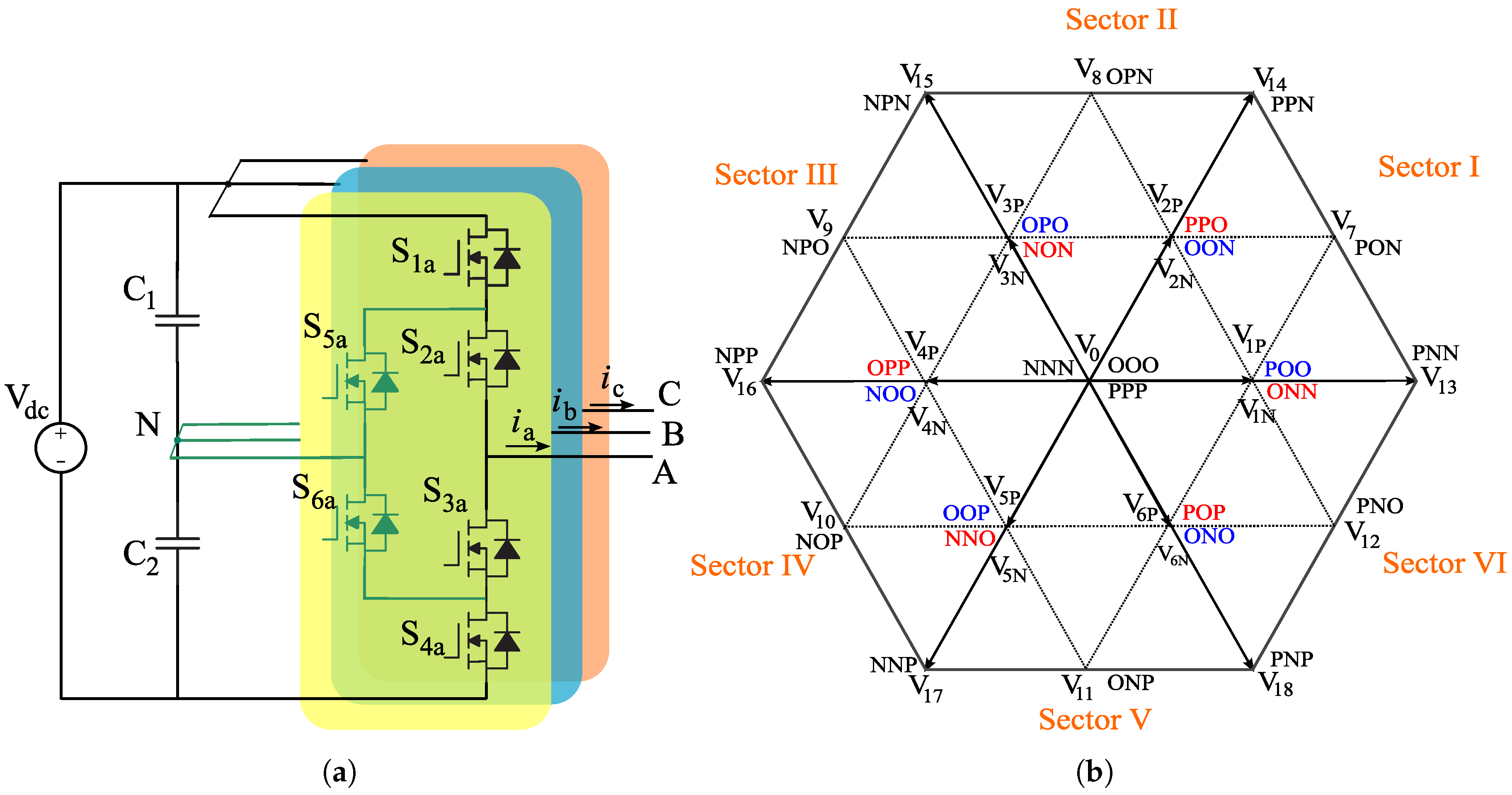
Figure 1.
(a) Topology of the ANPC and its (b) space vector diagram.
Figure 1.
(a) Topology of the ANPC and its (b) space vector diagram.
Figure 2.
(a) Virtual space vector diagram in sector I, (b) switching sequence of , resultant neutral-point current, NPV variations, and the generated . (Green: phase a; Red: phase b; Blue: phase c).
Figure 2.
(a) Virtual space vector diagram in sector I, (b) switching sequence of , resultant neutral-point current, NPV variations, and the generated . (Green: phase a; Red: phase b; Blue: phase c).
Figure 3.
Conventional CBPWM with two carriers.
Figure 3.
Conventional CBPWM with two carriers.
Figure 4.
Construction of the phase leg state using positive and negative modulation waves. (Green: negative modulation wave switching; Blue: positive modulation wave switching).
Figure 4.
Construction of the phase leg state using positive and negative modulation waves. (Green: negative modulation wave switching; Blue: positive modulation wave switching).
Figure 5.
Positive and negative modulation waves of phase A, .
Figure 5.
Positive and negative modulation waves of phase A, .
Figure 6.
Reversed switching patterns using two carriers with opposite phases.
Figure 6.
Reversed switching patterns using two carriers with opposite phases.
Figure 7.
Different combinations of switching sequences to reduce the CMV when the switching pattern is different for only (a) , (b) , and (c) , respectively.
Figure 7.
Different combinations of switching sequences to reduce the CMV when the switching pattern is different for only (a) , (b) , and (c) , respectively.
Figure 8.
Harmonic flux trajectories of (a) conventional CBPWM in Sector I, (b) double modulation RCMV-CBPWM when is reversed in all Sectors.
Figure 8.
Harmonic flux trajectories of (a) conventional CBPWM in Sector I, (b) double modulation RCMV-CBPWM when is reversed in all Sectors.
Figure 9.
RMS value of the HFT in a fundamental cycle for four different reversed switching combinations.
Figure 9.
RMS value of the HFT in a fundamental cycle for four different reversed switching combinations.
Figure 10.
Neutral-point current (rms) in the first Sector for unity power factor when (a) is reversed, (b) is reversed.
Figure 10.
Neutral-point current (rms) in the first Sector for unity power factor when (a) is reversed, (b) is reversed.
Figure 11.
Neutral-point current (rms) of the proposed hybrid modulation for unity power factor in the first Sector.
Figure 11.
Neutral-point current (rms) of the proposed hybrid modulation for unity power factor in the first Sector.
Figure 12.
Space vector diagram of the proposed hybrid CBPWM with reduced CMV.
Figure 12.
Space vector diagram of the proposed hybrid CBPWM with reduced CMV.
Figure 14.
Positive and negative compensating currents in Sector I when (a) , (b) .
Figure 14.
Positive and negative compensating currents in Sector I when (a) , (b) .
Figure 15.
Average positive and negative compensating currents under different power factors and modulation indices.
Figure 15.
Average positive and negative compensating currents under different power factors and modulation indices.
Figure 16.
The experimental setup of the 3-L ANPC.
Figure 16.
The experimental setup of the 3-L ANPC.
Figure 17.
Measured line-to-line voltage, DC-link capacitor voltages, output current , common-mode voltage , and harmonic content for Case I; (a) conventional CBPWM, (b) RCMV-CBPWM where only phase a is reversed, (c) proposed RCMV-CBPWM.
Figure 17.
Measured line-to-line voltage, DC-link capacitor voltages, output current , common-mode voltage , and harmonic content for Case I; (a) conventional CBPWM, (b) RCMV-CBPWM where only phase a is reversed, (c) proposed RCMV-CBPWM.
Figure 18.
Measured line-to-line voltage, DC-link capacitor voltages, output current , common-mode voltage , and harmonic content for Case II; (a) conventional CBPWM, (b) RCMV-CBPWM where only phase a is reversed, (c) proposed RCMV-CBPWM.
Figure 18.
Measured line-to-line voltage, DC-link capacitor voltages, output current , common-mode voltage , and harmonic content for Case II; (a) conventional CBPWM, (b) RCMV-CBPWM where only phase a is reversed, (c) proposed RCMV-CBPWM.
Figure 19.
Experimental results of voltage balancing control with the proposed method.
Figure 19.
Experimental results of voltage balancing control with the proposed method.
Table 1.
Switching states of a three-level ANPC.
Table 1.
Switching states of a three-level ANPC.
| Switching State | Device Switching Status | Output Phase Voltage |
|---|
| | | | | |
|---|
| [P] | 1 | 1 | 0 | 0 | 0 | 1 | |
| [O] | OU1 1 | 0 | 1 | 0 | 0 | 1 | 0 | 0 |
| OU2 1 | 0 | 1 | 0 | 1 | 1 | 0 |
| OL1 2 | 1 | 0 | 1 | 0 | 0 | 1 |
| OL2 2 | 0 | 0 | 1 | 0 | 0 | 1 |
| [N] | 0 | 0 | 1 | 1 | 1 | 0 | |
Table 2.
The effect of medium and small vectors on the NP.
Table 2.
The effect of medium and small vectors on the NP.
| Mediums Vectors | Small Vectors |
|---|
| | | | | |
| | | | |
| | | | | |
| | | | |
| | | | | |
| | | | |
Table 3.
Generated CMV by different space vectors.
Table 3.
Generated CMV by different space vectors.
| Vectors | | CMV |
|---|
| zero vector | (OOO) | 0 |
| zero vector | ((PPP), (NNN) | |
| small vectors1 | (POO), (OON), (OPO) | |
| (NOO), (OOP), (ONO) |
| small vectors2 | (ONN), (PPO), (NON) | |
| (OPP), (NNO), (POP) |
| medium vectors | (PON), (OPN), (NPO) | 0 |
| (NOP), (ONP), (PNO) |
| large vectors | (PNN), (PPN), (NPN) | |
| (NPP), (NNP), (PNP) |
Table 4.
Experimental parameters.
Table 4.
Experimental parameters.
| Symbol | Description | Value |
|---|
| input DC voltage | 200 V |
| switching frequency | 50 kHz |
| fundamental frequency | 833 Hz |
| DC-link capacitors | 72 F |
| m | modulation index | 0.75 |
| L | load inductance | 200 H |
| R | load resistance | 1 |
Table 5.
Harmonic content of CMV for case I.
Table 5.
Harmonic content of CMV for case I.
| | | | |
|---|
| conventional CBPWM | 31.2 | 1 | 2.04 |
| RCMV-CBPWM | 11.37 | 1.17 | 0.08 |
| proposed RCMV-CBPWM | 6.6 | 0.83 | 0.05 |
Table 6.
Harmonic content of CMV for case II.
Table 6.
Harmonic content of CMV for case II.
| | | | |
|---|
| conventional CBPWM | 32.6 | 0.68 | 2 |
| RCMV-CBPWM | 15.9 | 1.37 | 0.6 |
| proposed RCMV-CBPWM | 12.8 | 1.2 | 0.24 |


