Article

PCB Rogowski Coils for Capacitors Current Measurement in System Stability Enhancement

1
School of Automation, Wuhan University of Technology, Wuhan 430070, China
2
Three Gorges Intelligent Control Technology Co., Ltd., Wuhan 430070, China
*
Author to whom correspondence should be addressed.
Electronics 2023, 12(5), 1099; https://doi.org/10.3390/electronics12051099
Submission received: 14 January 2023 / Revised: 15 February 2023 / Accepted: 16 February 2023 / Published: 23 February 2023

Abstract

:
In terms of high-current measurement of capacitors, PCB Rogowski coils have attracted much attention because of their small size and easy installation. However, they are vulnerable to electromagnetic interference. In order to improve the immunity of the coil, this paper studies the influence of the structure and parameter changes of the double-layer PCB coil on the measurement accuracy of mutual inductance. By testing the frequency response of four common coil structures, a differential winding coil structure is proposed. Based on the measurement of large capacitance current, the influence of non-electrical parameters of coils on the measurement accuracy of mutual inductance is experimentally verified.

1. Introduction

Current measurements of capacitors have commonly used traditional current sensors [1,2,3,4,5,6,7,8,9,10,11], but they have some disadvantages. For example, Hall sensors have a large footprint and are expensive [12], which is not suitable for applications requiring small size and low cost. The shunt is cost-effective, but there are areas that cannot be measured without additional technology [13]. There is no good electrical isolation between the input and output, thus lowering the safety level [14]. Hall components have disadvantages such as magnetoresistance effect and temperature error. Its bandwidth is normally less than 1 MHz in order to avoid overheating caused by core losses [15]. The measurements are easily affected by location [16,17]. Rogowski coils have become a hotspot of current research due to their advantages such as no magnetic saturation, simple insulation, and wide measurement range.
The Rogowski coil was invented by the German scientist Rogowski. At the beginning of its invention, it could only be used for measuring magnetic fields since its induction electromotive force was very small and could not be used to drive secondary devices due to the technical limitations at that time. In 1963, Cooper, a British scholar, derived the transfer function of the Rogowski coil at high frequencies based on its high frequency characteristics, which laid the foundation for high-power pulse technology [18]. In 1966, by studying the structure of Rogowski coils, Ramboz improved the measurement accuracy by an order of magnitude [19]. With the rapid development of digital signal processing technology, Rogowski coils were widely used as the head structure for current sensors [20]. However, as conventional Rogowski coils are wound on a non-magnetic skeleton by hand or by winding machine, the uniformity of the winding density cannot be guaranteed and the cross-sectional areas of the coils may also not be equal. Therefore, the stability of the coil mutual inductance coefficient and the consistency of the distribution parameters cannot be guaranteed, resulting in Rogowski coils being hindered in industrial applications.
At the end of the twentieth century, the development of PCB technology provided new ideas for the development of traditional Rogowski coils [21,22,23,24,25,26,27,28,29,30,31,32,33,34,35,36,37,38,39], with its digital wiring and fully automated production methods that made it possible to reduce the dispersion of Rogowski coils. In 2000, N. Karrer proposed that PCB technology could be applied to Rogowski coils [21], using the characteristics of a double layer of copper foil wiring connected by through-holes to form the winding of coils. Since then, a variety of styles of PCB Rogowski coils have emerged, and most of them are based on a copper foil directly connected to a double-sided winding structure [22,23,24,25,26,27], which is a simpler PCB Rogowski coil wiring. This is not a completely symmetrical structure, and it has a large dispersion, so the anti-interference performance is poor. In Ref. [28], the author designed the outermost two layers of the coil as shielding grounding layers and proposed twisted pair type four-layer PCB Rogowski coils. The paper conducted a systematic study of four-layer PCB Rogowski coils and used the coils for switching current measurements of SiC devices in Ref. [29]. Although the additional shielding layer can effectively suppress electric field interference, four-layer PCBs undoubtedly greatly increase the application cost. A square PCB Rogowski coil with segmented turns was designed to increase the bend density and thus enhance the interference immunity in Ref. [30]. The authors in Ref. [31] applied PCB Rogowski coils for short-circuit protection of high-power SiC MOSFET devices. In Ref. [32], a coil structure with a C-shaped opening was proposed and used in a lightning-strike current detection system. In Ref. [33], PCB Rogowski coils were applied to a multi-conductor structure for high-current measurement systems. Hasegawa et al. integrated PCB Rogowski coil current sensors in IGBT modules to measure the output current of PWM inverters [34].
PCB Rogowski coils are widely used in current measurements and protection systems. However, there are still some challenges in coil design and research, such as the effect of the coil structure and wiring differences of PCB Rogowski coils on the mutual inductance coefficient, this impact has not been quantitatively analyzed from experiments.
In this paper, based on the analysis of four types of directly connected PCB Rogowski coils, we design frequency response experiments to quantitatively verify the influence of coil wiring structure on the measurement error of the mutual inductance coefficient. For this purpose, we propose to use a differential winding coil structure with a symmetrical structure and strong anti-interference performance. Finally, for the high-current measurement of capacitors, quantitative accuracy analysis and experimental verification are carried out from the perspective of structural parameters.

2. Working Principle of PCB Rogowski Coil

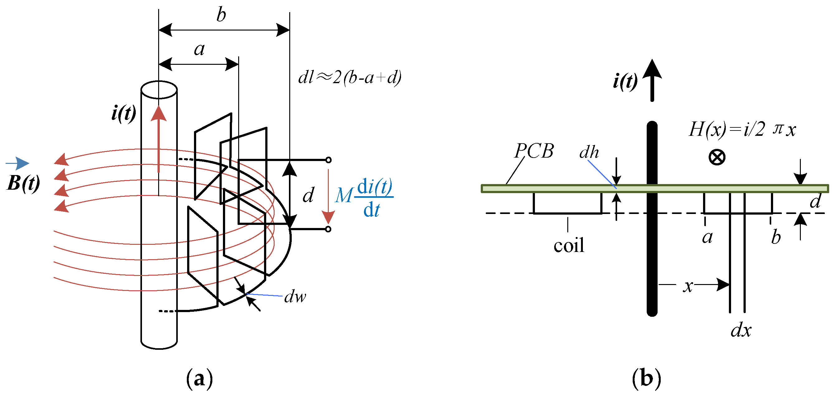
Conventional Rogowski coils are constructed by uniformly winding N turns of a coil on a non-magnetic skeleton of constant cross-sectional area, in which the winding returns to the starting point along the central axis of the winding. Figure 1 shows a sketch of the structure of a Rogowski coil uniformly wound on a circular skeleton. Its working principle is based on the law of electromagnetic induction and Ampere’s law of loops. When the alternating primary current passes vertically through the center of the coil, a magnetic field is generated around the current, and the alternating magnetic induction lines induce an electric potential at both ends of the line turns, which is proportional to the rate of change of the primary current against time. The PCB Rogowski coil is wound on the copper-coated plate, but it works the same way as the traditional Rogowski coil. Figure 2 is the structure of the PCB Rogowski coil [40].
When the magnitude of the current-carrying conductor i(t) changes, the induced electric potential of the N-turn coil is:
e ( t ) = N d φ ( t ) d t                                                   = N μ 0 d 2 π x ln b a d i ( t ) d t               = M d i ( t ) d t
where e t is the induced electric potential of the N -turn coil, d is the thickness of PCB, μ 0 = 4 π × 10 7 H/m is the vacuum permeability, x is the distance between a point on the wire turn and the axis of the primary conductor, a and b are the inner and outer diameters of the coil, respectively, and the mutual inductance coefficient M of the PCB Rogowski coil is:
M = N μ 0 d 2 π ln b a
From Equation (1), it can be seen that the induced electric potential of the coil is proportional to the differentiation of the current-carrying conductor with respect to time, with a scale factor of M .
Due to the influence of the coil distribution parameters, the magnitude of the output voltage across the PCB Rogowski coil is not equal to the magnitude of the induced electromotive force of the coil. Figure 3 shows the most commonly used lumped parameter model of the Rogowski coil, where the voltage source represents the induced electromotive force of the coil to the measured current, and it is connected in series with the coil self-inductance L c , the coil internal resistance R c , and the distribution capacitance C c .
The following equations are used to calculate these equivalent parameters [40,41]:
L c = μ 0 N 2 d 2 π ln b a
R c = N × ρ × d l d w × d h
C c = 4 π 2 ε 0 b + a log b + a b a
where ρ is the wire resistivity, 1.7 × 10⁻⁸ Ω·m, d l is the length of the coil per turn, d w is the coil alignment width, d h is the PCB copper thickness, and ε 0 is the vacuum dielectric constant, 8.854 × 10⁻¹² F/m.
From the parameter model shown in Figure 3, the transfer function of the PCB Rogowski coil can be deduced as:
U I = s M L c C c s 2 + R c C c s + 1
The transfer function of the Rogowski coil shows that its output voltage is proportional to the current, and the proportionality factor is a second-order polynomial function. Among them, the mutual inductance coefficient M directly affects the measurement accuracy, sensitivity, and interference resistance of PCB Rogowski coils. Therefore, the mutual inductance between the Rogowski coil and the conductor under test is the primary factor to be considered in the actual design. The mutual inductance factor M is not only related to the coil size parameters, such as the number of turns N , coil inner diameter a , coil outer diameter b , or the PCB thickness, but also to the coil structure.

3. Coil Structure

The structure of the PCB Rose coil is integrated into the printed circuit board, and its wire turns are composed of traces on the top and bottom layers and vias, forming a rectangular cross-section. Different winding methods produce different coil structures. In view of the problem that various coil structures have different effects on measurement accuracy, this section studies four common double-layer PCB Rogowski coil structures and theoretically analyzes their immunity. Then a differential wound coil structure is proposed. Based on the coil size limitation, the influence of structural parameters on the mutual inductance coefficient is studied.

3.1. Four Types of Double-Layer Coils

Figure 4 shows the structure of a double-layer PCB Rogowski coil with four different winding methods.
Coil 1 connects the top (red) alignment to the bottom (blue) alignment through holes on the inside and outside [42], with a rectangular wire turn cross-section. This coil has a relatively simple wiring structure, but the individual wire turns formed by the top and bottom alignments are not centrally symmetrical, and no return loop is provided. Coil 2 improves the above defects. The bottom layer straight trace of this structure (covered by the top layer straight traces) is connected to the top layer straight trace through the through-hole and forms an arc with radius b and arc of 2π/2N clockwise. The bottom (blue) arc is connected to the top (red) arc by an outer via, so the symmetry of the line turns formed in this way is strong. However, because no return loop is set, the connected N-turn coil is equivalent to a large wire turn of radius b on the outside. When the magnetic field perpendicular to the PCB plane generated by the external interference current crosses the PCB coil plane, an interference-induced voltage is generated.
To solve this problem, coil 3 adds a return loop on the basis of coil 2 to offset the influence generated by external interference currents. However, the radius of the return loop is bigger than the outer diameter of the coil, and the interference magnetic field generated by the interference current is not completely offset. For this reason, coil 4 changes the wiring of the forward loop, making the arc trace of the underlying trace in the forward loop protrude a piece, thereby increasing the area of the large wire turns formed by the forward loop. This wiring makes the area of the large wire turns formed by the forward loop and the return loop equal and theoretically offsets the impact of interference currents.

3.2. Differential Winding Coils

Since the PCB Rogowski coils discussed in this paper are integrated into the cylindrical large capacitor, to some extent, they will be limited by the size of the coil, and the number of coil turns will also be limited. The measurement accuracy is susceptible to interference from external electromagnetic fields. For this reason, a coil differential winding structure is proposed in Ref. [40].
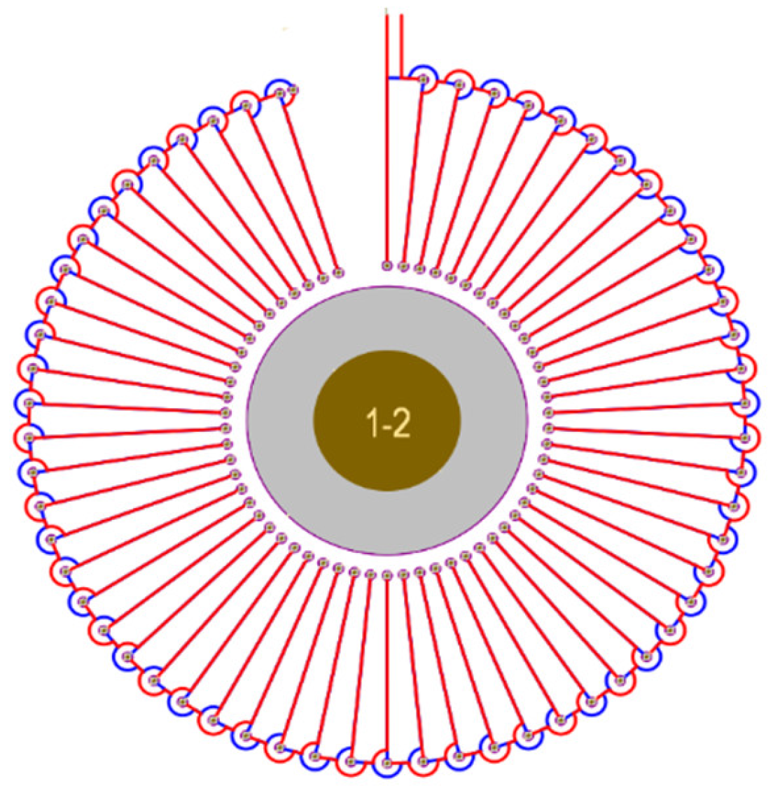
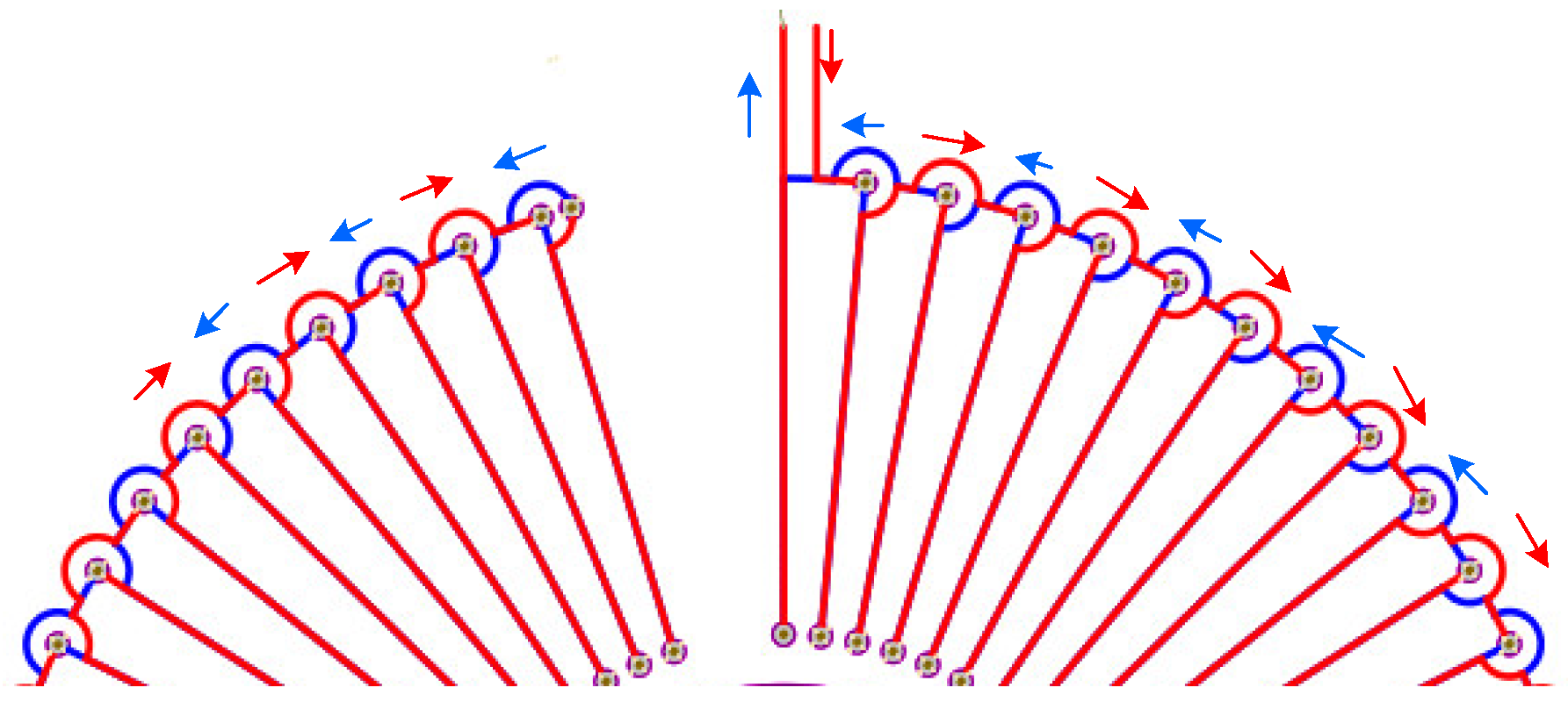
The coil structure, shown in Figure 5, allows the wire turns to be wound not only in the same direction, but the return loop is also wound in the reverse direction in the same way, i.e., the return loop also has N turns of coils. Figure 6 shows a partial enlargement of the differential winding coil, with the red and blue alignments representing the top and bottom layers respectively. The red arrow is the direction of the arc trace in the forward loop, and the blue arrow represents the return path of the line turn. The top and bottom traces form a differential winding structure through vias. Due to the symmetrical structure, this coiled structure is highly resistant to external interference.
When PCB Rogowski coils are used for high-current measurement of capacitors, they are inevitably subject to capacitive coupling interference with large voltage gradients [43]. When there is capacitive coupling interference, the capacitive displacement current will flow through the coil thus causing interference. At this time, the induced electromotive force of the coil can be divided into the induced electromotive force of the measured signal and the induced electromotive force of the interference current. In Figure 5, the induction electromotive force of the coil is the sum of the induction electromotive force in the forward and return loops. Since the forward and return loops are wound in opposite directions, the direction of the induced electromotive force caused by the magnetic flux of the measured current is also opposite. Because the disturbance generated by the capacitive displacement current is not generated by the magnetic field of the conductor under test, the voltage drop does not depend on the winding direction of the PCB Rogowski coil. As shown in Equations (7) and (8),
e f o r t h t = e s t + e c t = M d i t d t + M c d i c t d t
e b a c k t = e s t + e c t = M d i t d t + M c d i c t d t
where e f o r t h t is the induced electromotive force of the forward loop, e b a c k t is the induced electromotive force of the return loop, e s t is the induced electromotive force of the measured current, e c t is the induced electromotive force due to capacitive coupling interference, M c is the mutual inductance coefficient between the capacitive displacement current and the coil, and i c is the capacitive displacement current.
Therefore, the total induced voltage of the coil is:
e m e a s u r e t = e f o r t h t e b a c k t = 2 M d i t d t
The interference of the capacitive displacement current to the induced voltage of the differential winding coil can be completely neutralized and the induced electric potential of the coil is twice as high as that of the single loop because the winding direction of the return loop is opposite to that of the forward loop.

3.3. Influence of Structural Parameters

The influence of structural parameters on the coil is mainly reflected in the influence on the size of the mutual inductance coefficient M . Therefore, reasonable structural parameters need to be designed to ensure the maximum mutual inductance coefficient. From Equation (2), the mutual inductance coefficient is proportional to the number of turns of the coil N , PCB thickness d , and the logarithm of b / a .
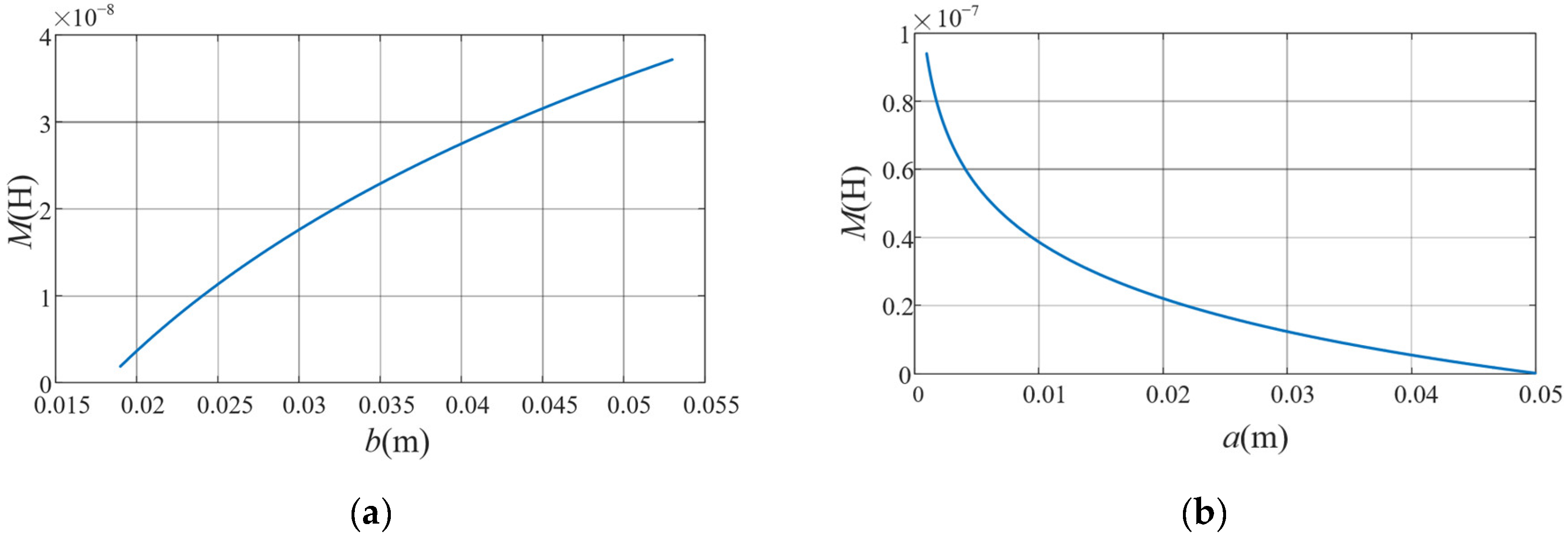
Figure 7 shows the effect of a single variable on the mutual inductance value. When the values of the number of coils turns N , PCB thickness d , and inner diameter a are fixed, the curve of mutual inductance value with outer diameter b is shown in Figure 7a. Obviously, the larger the outer diameter, the larger the mutual inductance coefficient. Figure 7b shows the variation curve of the mutual inductance value with inner diameter a, and the mutual inductance value decreases as the inner diameter a increases. For the differential winding coil structure, the number of turns N will be limited due to the presence of arced traces on the outside of the coil and the minimum diameter constraint of the inner vias. The research of this paper is the application of PCB Rogowski coils to the condition monitoring of capacitors, thus the size of the coil depends, to some extent, on the size of the capacitor surface. In this section, the influence of the structural parameters of the coil will be illustrated with the example of a cylindrical film capacitor.
Due to the limitation of the PCB manufacturing process, the maximum board thickness d is taken as 2 mm. The shortest distance of one of the terminals of this film capacitor from the edge is 27.5 mm, and the PCB Rogowski coil is screwed on the capacitor terminal. Therefore, considering the safety distance from PCB alignment to the outer frame line and setting a certain margin, the outer diameter b of the coil can be set as 52 mm. According to the dimensional constraint relationship of the differential winding coil (Figure 8), set the inner diameter of the coil a as the independent variable. A safety distance needs to exist between the inner through-holes and the arc alignment, so the number of coil turns N will also be limited by the inner diameter a . Equations (10) and (11) need to be met at the same time.
N 2 π 2 s i n 1 x 2 a
b s i n 2 π 2 N > 2 r 1 + 0.254
where x is the minimum distance between adjacent through-holes on the inside. Due to PCB manufacturer process limitations, the minimum through-hole spacing Δ x is 0.127 mm. Set the PCB through-hole pad diameter to 0.508 mm, then x = 0.508   mm + 0.127   mm . r 1 is the radius of the outer circular arc alignment.
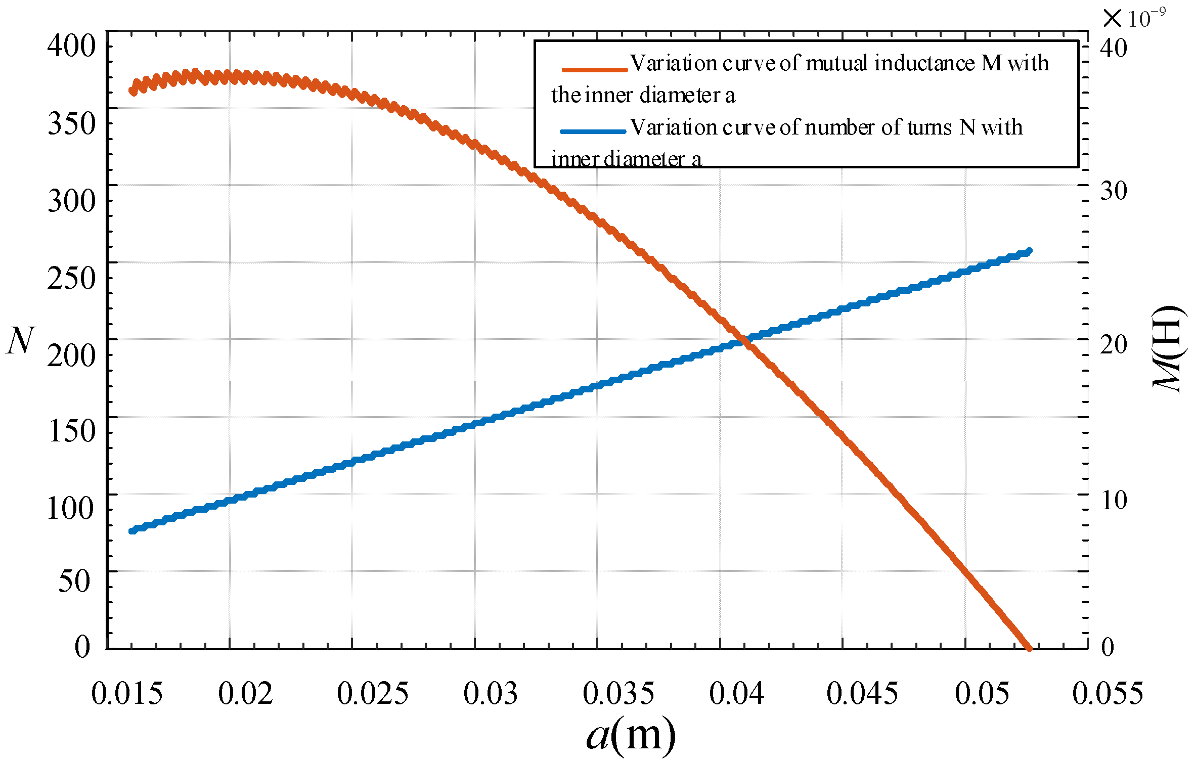
Therefore, when the value of the outer diameter b is fixed, both the number of turns N and the mutual inductance coefficient of the coil will be affected by the inner diameter a. According to the coupling relationship between Equations (10) and (11), the change curve is shown in Figure 9. The number of coil turns N increases linearly with the increase of inner diameter a, while the mutual inductance coefficient M becomes larger first and then decreases with the increase of inner diameter. Theoretically, when a is 18.6 mm, N is 90 and the mutual inductance coefficient can reach the maximum. At this time, the radius r 1 of the outer arc of the coil is 0.8 mm, which can also meet Equation (11).

4. Experiment Verification

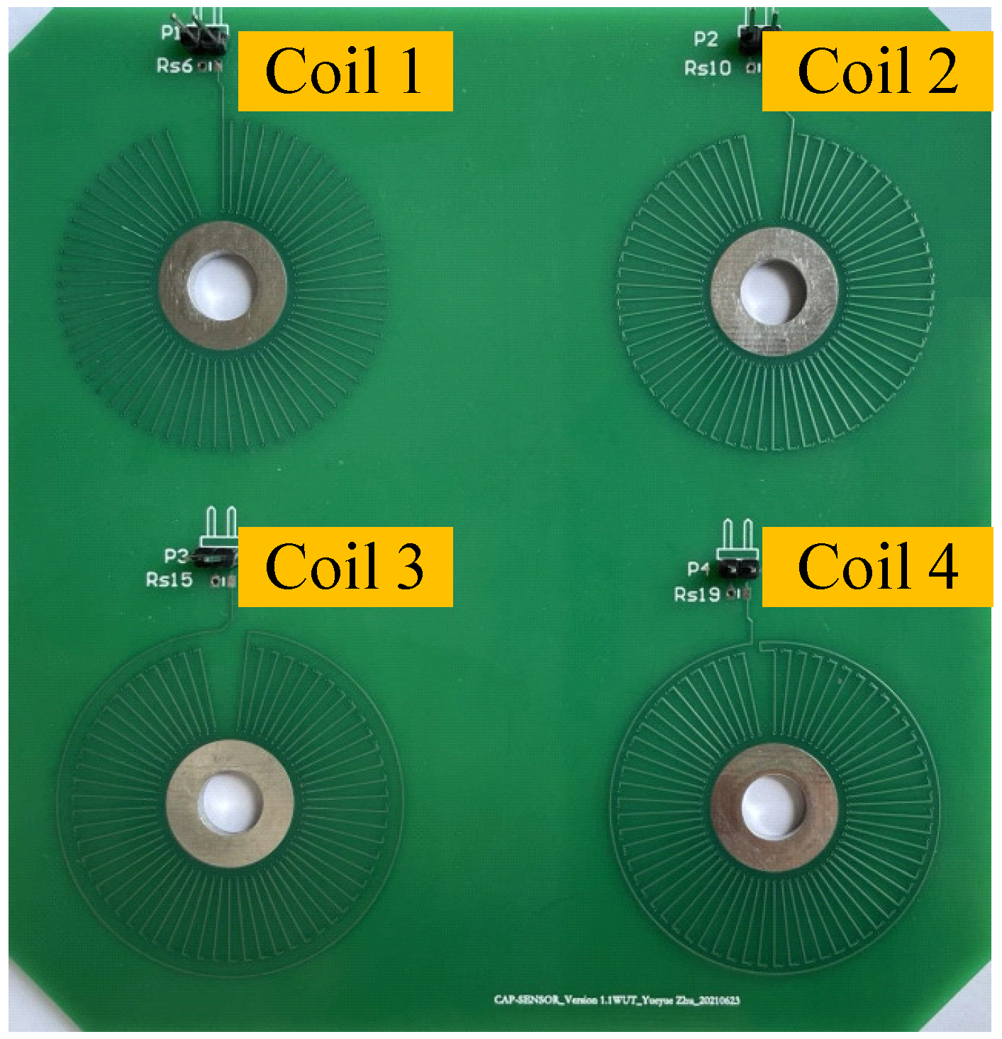
In order to verify the influence of the four coil structures on the measurement accuracy of PCB Rogowski coils, this paper sets the four coils to the same geometric parameters and sets the number of turns to 60 turns. Moreover, the mutual inductance coefficient M , coil self-inductance, coil internal resistance, and coil distributed capacitance are calculated from Equations (2)–(5), and the structural and electrical parameters of the four coils are detailed in Table 1 and Table 2. It can be seen that the geometric and electromagnetic parameters of the four coils are similar, except for the different ways of coil wiring. The four different coil structures are drawn in Altium Designer software according to the coil structure and the coil data in Table 1, and the physical drawings are shown in Figure 10.
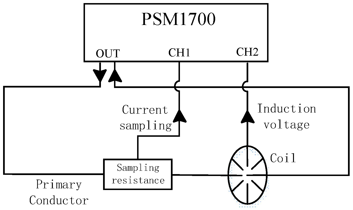
In order to test the characteristics of the coils with different winding methods, the experiments were conducted by using the PSM1700 frequency response analyzer and calculating the mutual inductance coefficients of the coils. This experiment does not apply additional shielding measures to the coil, nor does it integrate and signal process the output of the coil, and the experimental frame diagram is shown in Figure 11. Among them, the PSM1700 frequency response analyzer comes with a signal generator function, and the sine wave signal output from its output is used as the primary current input of the coil. The output wire of the PSM1700 is passed vertically through the center of the PCB coil, and the CH1 channel of the PSM1700 is used to collect the primary current signal through the sampling resistor, CH2 collects the output signal of the coil, and a Bode plot of the coil transfer function is displayed on the instrument panel. In this case, the sampling resistor is a 1 Ω high-precision sampling resistor.
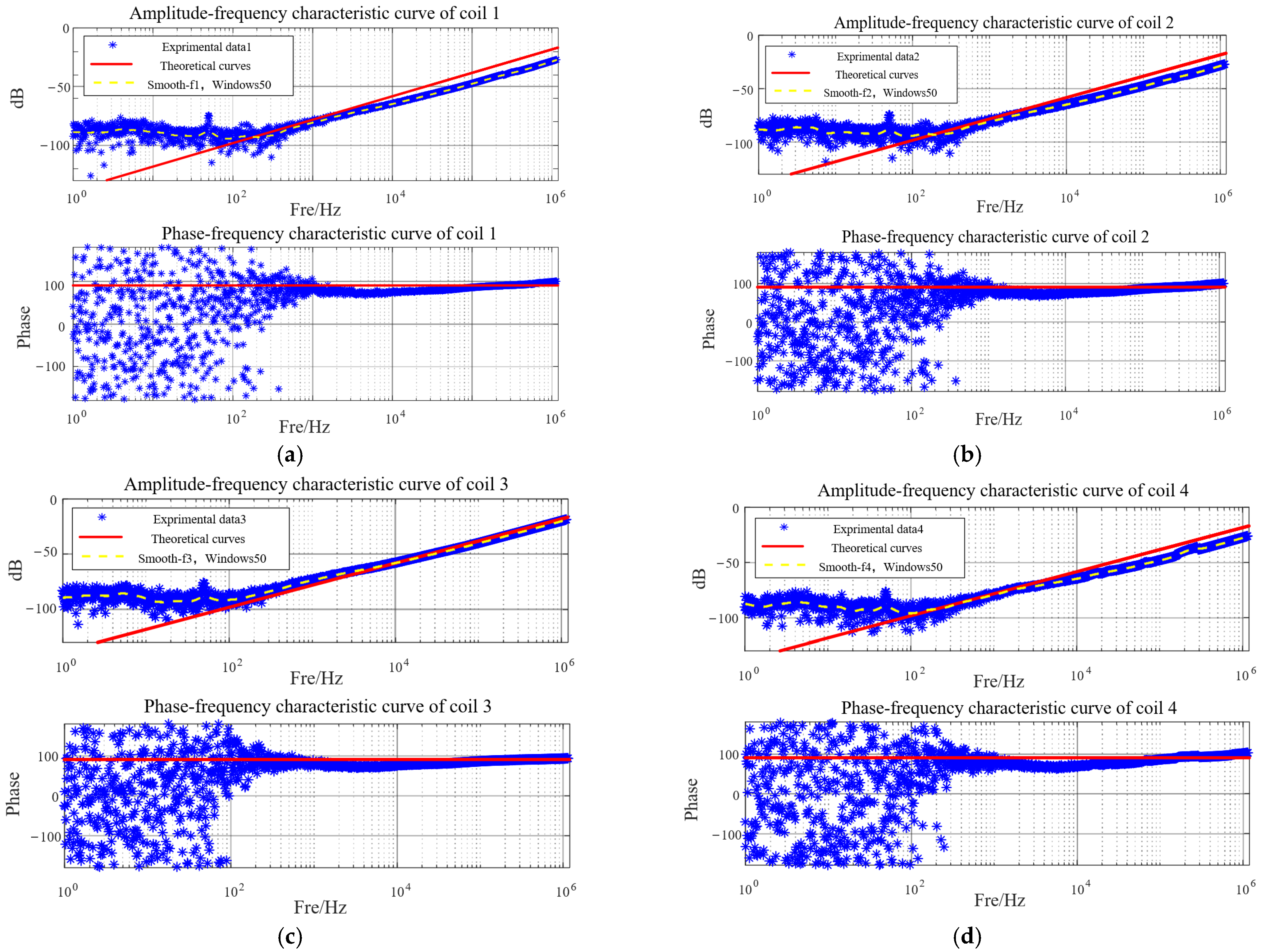
Figure 12 shows the amplitude-frequency characteristics of the frequency response of the four coils. The blue dots are the experimentally measured waveforms. The red solid line is the theoretical curve. The yellow dashed line is the curve after smoothing the experimental data.
The frequency response of all four coils at low frequencies (below 1 kHz) is not ideal, and coil 3, after 100 Hz, has a better fit than coils 1, 2, and 4. The mutual inductance values of all four coils are at the nH level. The output current of the signal generator in the experiment is 1.87 A. Therefore, the induced voltage of the coils at low frequencies is at the μV level, and the accuracy of the frequency response analyzer is not enough to detect the tiny voltage signal. Therefore, the amplitude-frequency characteristics and the phase frequency characteristics of the four coils in Figure 12 before 1 kHz are chaotic. The amplitude-frequency characteristic curves of coils 1–4 have a better fit after 1 kHz, and their phase-frequency characteristic curves show that the phase after 1 kHz is basically around 90°, which is consistent with the theoretical curve. In addition, the amplitude-frequency characteristic curve of coil 3 is closer to the theoretical curve. In order to present the influence of the Rogowski coil structure on the measurement error more intuitively, this paper derives the theoretical amplitude-frequency characteristic curve and does a linear fit to the experimental data to obtain the mutual inductance measurement values under different coil structures.
Since the parasitic parameters of the coil are small, the effects of coil inductance, coil internal resistance, and parasitic inductance can be neglected, and the transfer function of Equation (6) can be simplified to Equation (12):
H s = U s I s = M s
This formula leads to:
H ( f ) = j 2 π f M
Therefore, the theoretical amplitude-frequency characteristic curve is
D B f = 20 l g H = 20 l g M 2 π f = 20 l g f + 20 l g M 2 π
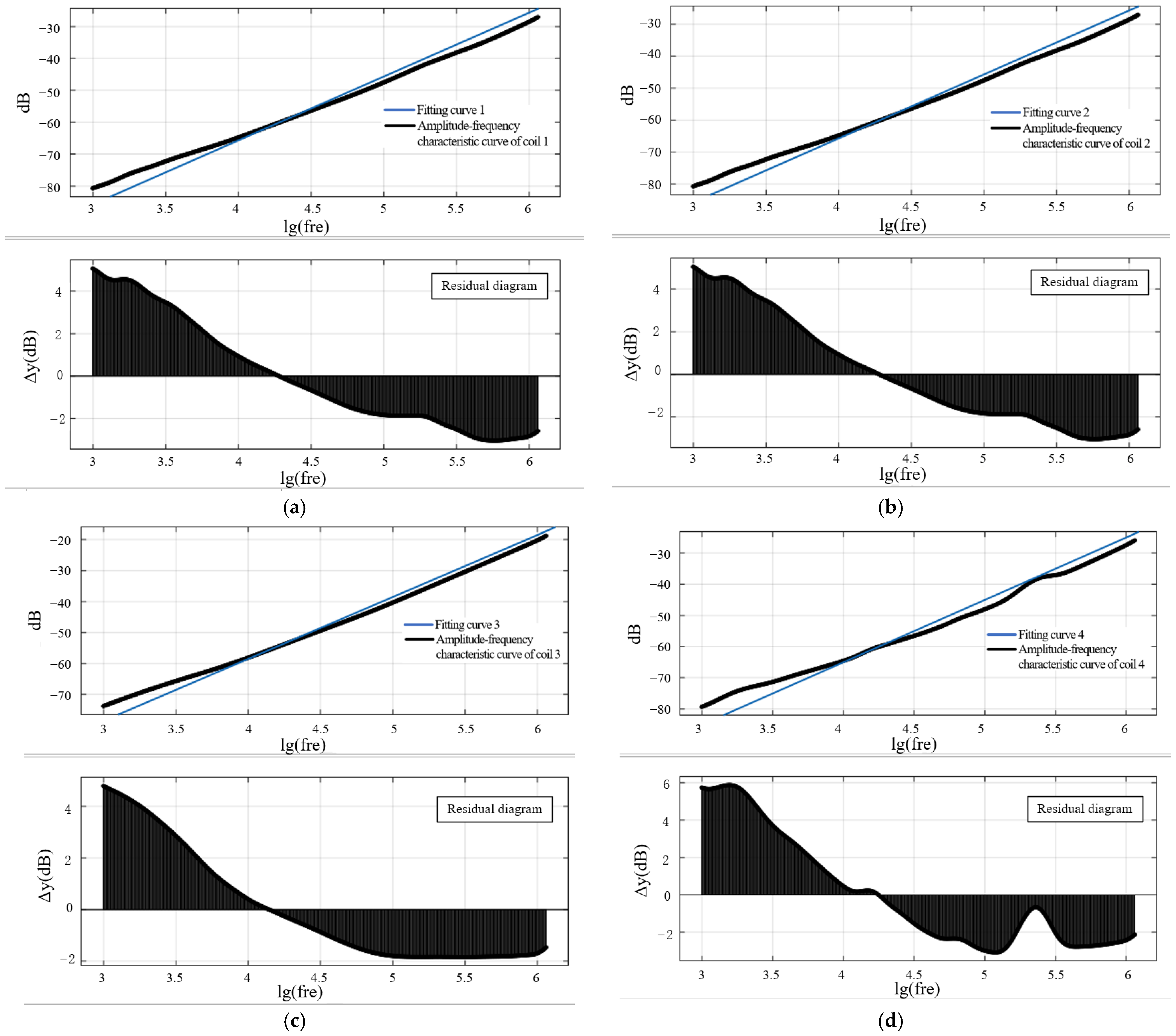
Theoretically, the transfer function of the coil should be a straight line with a slope of 20 dB/decade frequency, and the longitudinal intercept of the line is related to the mutual inductance value. Therefore, to obtain the mutual inductance coefficients of the coils more intuitively, the experimental data of the four coils 1 kHz–1.2 MHz were linearly fitted in Matlab, and the fitting function was set as
y = 20 l g x + b
where x is the frequency, y is the amplitude of the amplitude-frequency characteristic curve, and b is the longitudinal intercept. Then, the measured mutual inductance coefficient can be calculated by Equation (16).
M = 10 b 20 2 π
Figure 13 shows the fitted and residual results of the amplitude-frequency characteristic curves of coils 1–4 after the logarithmic transformation of the horizontal coordinates. It seems that the error between the fitting result of coil 4 and the measured result is the largest, the error of coil 3 is smaller than that of coil 1 and coil 2. Table 3 shows the measured mutual inductance values obtained from the fitted curves, where the mutual inductance values of coils 1 and 2 have a large error, coil 3 has an error of −29.4%, and coil 4 has the smallest relative error of −26.9%.
Analyzing the experimental results in Figure 12 and Figure 13, and Table 3, the following conclusions can be obtained. In terms of linearity, Coils 1–3 are smoother, while Coil 4, which has a theoretically symmetrical coil structure and better immunity, has poorer linearity instead. Due to coil 4′s complex wiring structure, makes its PCB alignment appear more right angles, resulting in interference in the coil response. In terms of mutual inductance accuracy, coil 1 and coil 2 are more susceptible to interference due to the absence of a return loop, with an error of −55%, while coil 4 has a slightly smaller mutual inductance error compared to coil 3 due to the equal area of the forward and return loops. Therefore, the coils with symmetrical structures and equal areas of the forward and return loops have relatively small errors in the mutual inductance coefficient.
The frequency response characteristics of differential winding coils with different inner and outer diameter values are measured experimentally below.
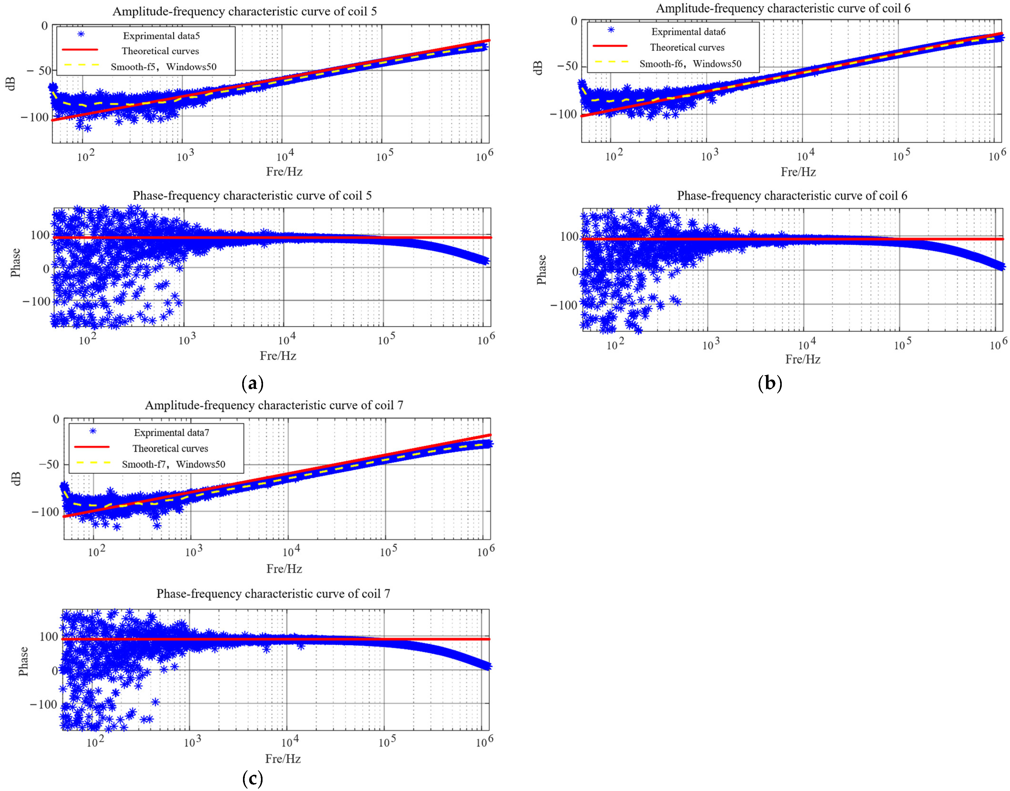
Table 4 and Table 5 show the structural and electrical parameters of the three coils with different inner and outer diameters. The frequency response characteristics measured using PSM1700 are shown in Figure 14.
The measured curves of the amplitude-frequency characteristic curve and phase-frequency characteristic curve are consistent with the theoretical curve in the frequency range of 1 kHz to 100 kHz. The phase frequency characteristic curve decreases slightly after 100 kHz, which is caused by the coupling capacitance, and the higher the frequency, the more obvious this phenomenon is. Moreover, since the mutual inductance coefficient M is at the nH level, even a large measurement error is not obvious on the Bode plot. Therefore, it is necessary to fit the experimental data of these three coils in a curve and calculate the experimental value of the mutual inductance coefficient M to obtain the measurement error.
The calculated values of mutual inductance coefficient M obtained by curve fitting are shown in Table 6. If coil 5 is used as the experimental control group, coil 6 is the experimental group with an 11.6 mm increase in outer diameter and coil 7 is the experimental group with a 2 mm increase in inner diameter. As can be seen from Table 6, the theoretical mutual inductance value of coil 6 is larger than that of coils 5 and 7, and its experimentally measured error value is relatively smaller. Therefore, when the differential winding coil is used for the measurement of capacitor ripple current, it is very important to maximize the use of the capacitor surface size and design reasonable structural parameters to maximize the mutual inductance coefficient.

5. Conclusions

The frequency response curves of four directly connected double-layer PCB coils illustrate that coils with return loops and a symmetrical structure can reduce the influence of interfering magnetic fields on the accuracy of mutual inductance coefficient measurements. Based on the high-current measurements of capacitors, the proposed differential winding coil structure has stronger anti-interference ability and higher accuracy of mutual inductance coefficient. However, due to its more complex wiring, there is inevitable capacitive coupling interference at high frequencies, which affects the accuracy of the coil measurement results at high frequencies. Experiments show that when the differential winding coil is applied to cylindrical capacitors, reasonable use of the capacitor surface size and design of the coil structure parameters can maximize the mutual inductance coefficient, which can improve the accuracy and immunity of the coil mutual inductance coefficient to a certain extent.

Author Contributions

Conceptualization, X.D.; methodology, X.Y. and Q.W.; formal analysis, G.Z., J.V.W. and Q.W.; investigation, X.Y. and Q.W.; writing—original draft preparation, X.Y.; writing—review and editing, G.Z., J.V.W., X.D. and Q.W.; funding acquisition, G.Z. All authors have read and agreed to the published version of the manuscript.

Funding

This research was funded by National Natural Science Foundation of China, grant number 51777146 and 51977163.

Data Availability Statement

No new data were created or analyzed in this study. Data sharing is not applicable to this article.

Conflicts of Interest

The authors declare no conflict of interest.

References

  1. Blaabjerg, F.; Pedersen, J.K.; Jaeger, U.; Thoegersen, P. Single current sensor technique in the DC link of three-phase PWM-VS inverters. IEEE Trans. Ind. Appl. 1997, 33, 1241–1253. [Google Scholar] [CrossRef]
  2. Ziegler, S.; Woodward, R.C.; Iu, H.; Borle, L.J. Current sensing techniques: A review. Sensors 2009, 9, 354–376. [Google Scholar] [CrossRef]
  3. Aiello, O.; Fiori, F. A new current sensor based on MagFET highly immune to EMI. In Proceedings of the 2009 International Conference on Electromagnetics in Advanced Applications, Turin, Italy, 14–18 September 2009; pp. 784–787. [Google Scholar]
  4. Sun, K.; Wei, Q.; Huang, L.; Matsuse, K. An Overmodulation Method for PWM-Inverter-Fed IPMSM Drive with Single Current Sensor. IEEE Trans. Ind. Electron. 2010, 57, 3395–3404. [Google Scholar] [CrossRef]
  5. Aiello, O.; Grovetti, P.; Fiori, F. Investigation on the susceptibility of hall-effect current sensors to EMI. In Proceedings of the EMC Europe 2011, York, UK, 26–30 September 2011; pp. 368–372. [Google Scholar]
  6. Ouyang, Y.; He, J.; Hu, J.; Wang, S.X. A current sensor based on the giant magnetoresistance effect: Design and potential smart grid applications. Sensors 2012, 12, 15520–15541. [Google Scholar] [CrossRef] [PubMed]
  7. Aiello, O.; Fiori, F. A New MagFET-Based integrated current sensor highly immune to EMI. Microelectron. Reliab. 2013, 53, 573–581. [Google Scholar] [CrossRef]
  8. Aiello, O.; Fiori, F. A new mirroring circuit for power MOS current sensing highly immune to EMI. Sensors 2013, 13, 1856–1871. [Google Scholar] [CrossRef] [Green Version]
  9. Aiello, O. Hall-effect current sensors susceptibility to emi: Experimental study. Electronics 2019, 8, 1310. [Google Scholar] [CrossRef] [Green Version]
  10. Lim, H.J. Current Detection Technique Using DC-Shunt and FET Voltage Drop of Three Phase Inverter; Kookmin University: Seoul, Republic of Korea, 2020. [Google Scholar]
  11. Jena, M.R.; Mohanty, K.B. Maximum efficiency controller for IPMSM using single DC link current sensor. In Proceedings of the 2020 IEEE International Symposium on Sustainable Energy, Signal Processing and Cyber Security (iSSSC), Gunupur Odisha, India, 16–17 December 2020. [Google Scholar]
  12. Tong, Q.; Chen, C.; Zhang, Q.; Zou, X. A Sensorless Predictive Current Controlled Boost Converter by Using an EKF with Load Variation Effect Elimination Function. Sensors 2015, 15, 9986–10003. [Google Scholar] [CrossRef] [Green Version]
  13. Hwang, J.-Y.; Park, J.-H.; Choi, J.-H.; Uhm, J.-I.; Lee, G.-H.; Lim, H.-S. A Precise Current Detection Method Using a Single Shunt and FET Rds(on) of a Low-Voltage Three-Phase Inverter. Electronics 2022, 11, 9. [Google Scholar] [CrossRef]
  14. Min, R.; Chen, C.; Zhang, X.; Zou, X.; Tong, Q.; Zhang, Q. An Optimal Current Observer for Predictive Current Controlled Buck DC-DC Converters. Sensors 2014, 14, 8851–8868. [Google Scholar] [CrossRef] [Green Version]
  15. Asada, T.; van Wyk, J.D.; Xiao, C.; Odendaal, W.G.; Zhao, L. An overview of integratable current sensor technologies. In Proceedings of the 38th IAS Annual Meeting on Conference Record of the Industry Applications Conference, Salt Lake City, UT, USA, 12–16 October 2003; pp. 1251–1258. [Google Scholar]
  16. Lu, C.; Ren, H.; Lei, S.; Wang, X.; Yuan, G. Principle and application of TMR anti-DC current sensor. Electr. Meas. Instrum. 2022, 59, 126–132. [Google Scholar]
  17. Zhang, H.; Li, Y.; Liu, J. Design of magnetic ring for open-close Hall sensor for calibration. Electr. Meas. Instrum. 2022, 59, 171–175. [Google Scholar]
  18. Cooper, J. On the high-frequency response of a Rogowski coil. J. Nucl. Energy Part C Plasma Phys. Accel. Thermonucl. Res. 1963, 5, 285. [Google Scholar] [CrossRef]
  19. Ramboz, J.D. Machinable Rogowski coil, design, and calibration. IEEE Trans. Instrum. Meas. 1996, 45, 511–515. [Google Scholar] [CrossRef]
  20. Ward, D.A. Measurement of Current Using Rogowski Coils. Proc. IEE Colloq. Instrum. Electr. Supply Ind. 1993, 1, 1–3. [Google Scholar]
  21. Ward, D.A.; Exon, J. Using Rogowski Coils for Transient Current Measurements. Eng. Sci. Educ. J. 1993, 2, 105–113. [Google Scholar] [CrossRef]
  22. Karrer, N.; Hofer-Noser, P. PCB Rogowski coil for high di/dt current measurement. In Proceedings of the 2000 IEEE 31st Annual Power Electronics Specialists Conference, Galway, Ireland, 23 June 2000; pp. 1296–1301. [Google Scholar]
  23. Kojovic, L.A. PCB Rogowski coil designs and performances for novel protective relaying. In Proceedings of the 2003 IEEE Power Engineering Society General Meeting (IEEE Cat. No. 03CH37491), Toronto, ON, Canada, 13–17 July 2003; Volume 2. [Google Scholar]
  24. Yang, N.; Duan, X. A new Rogowski coil-PCB Rogowski coil. High Volt. Electr. Appl. 2005, 41, 209211. [Google Scholar]
  25. Robles, G.; Argueso, M.; Sanz, J.; Giannetti, R.; Tellini, B. Identification of parameters in a Rogowski coil used for the measurement of partial discharges. In Proceedings of the 2007 IEEE Instrumentation & Measurement Technology Conference IMTC 2007, Warsaw, Poland, 1–3 May 2007. [Google Scholar]
  26. Tao, T.; Zhao, Z.; Ma, W.; Pan, Q.; Hu, A. Design of PCB Rogowski coil and analysis of anti-interference property. IEEE Trans. Electromagn. Compat. 2016, 58, 344–355. [Google Scholar] [CrossRef]
  27. Wang, J.; Chen, W.; Chen, P. A Design Method of PCB Rogowski Coil in limited space and modified integral circuit. IEEE Sens. J. 2020, 20, 5801–5808. [Google Scholar] [CrossRef]
  28. Xu, Z.; Ming, L.; Shi, Y.; Xin, Z.; Lu, B. Switching current measurement of silicon carbide devices based on twisted pair four-layer PCB Rogowski coil. J. Mot. Control 2021, 25, 46–57. [Google Scholar]
  29. Ming, L.; Xin, Z.; Yin, C.; Loh, P.C.; Liu, Y. Screen-returned PCB Rogowski coil for the switch current measurement of SiC devices. In Proceedings of the 2019 IEEE Applied Power Electronics Conference and Exposition (APEC), Anaheim, CA, USA, 17–21 March 2019. [Google Scholar]
  30. Fu, S.; Zhang, G.; Zhan, Y.; Peng, C.; Zhao, Z.; Li, X.; Cui, X. Method of segmented turns arrangement of PCB Rogowski coil with anti-interference ability. IEEE Trans. Instrum. Meas. 2021, 70, 1–12. [Google Scholar] [CrossRef]
  31. Chen, L. Research on Characteristics and Drive Protection of High Power SiC MOSFET Devices; Beijing Jiaotong University: Beijing, China, 2019. [Google Scholar]
  32. Wei, W.; Cai, L.; Zhang, C. Design of C type multilayer lightning current detector based on PCB Rogowski coil. J. Sichuan Inst. Technol. Nat. Sci. Ed. 2019, 32, 29–34. [Google Scholar]
  33. Gu, P.-Y.; Chen, Q.; Li, H.-B.; Hu, C.; Gong, H.; Jiao, Y. PCB Rogowski coils for 300 kA current measurement on a multi-split conductor. IEEE Sens. J. 2019, 19, 6786–6794. [Google Scholar] [CrossRef]
  34. Hasegawa, K.; Sho, S.; Tsukuda, M.; Omura, I.; Ichiki, M.; Kato, T. Output-current measurement of a PWM inverter with a tiny PCB rogowski sensor integrated into an IGBT module. In Proceedings of the 2019 IEEE Energy Conversion Congress and Exposition (ECCE), Baltimore, MD, USA, 29 September–3 October 2019. [Google Scholar]
  35. C37.235-2007; IEEE Guide for the Application of Rogowski Coils Used for Protective Relaying Purposes. IEEE: New York, NY, USA, 2007.
  36. Mingotti, A.; Peretto, L.; Tinarelli, R. Smart characterization of rogowski coils by using a synthetized signal. Sensors 2020, 20, 3359. [Google Scholar] [CrossRef]
  37. Riehl, R.R.; de Castro, B.A.; Fraga, J.R.C.P.; Puccia, V.; Lucas, G.B.; Andreoli, A.L. Assessment of Rogowski Coils for Measurement of Full Discharges in Power Transformers. Eng. Proc. 2021, 10, 16. [Google Scholar]
  38. Tan, Q.; Zhang, W.; Tan, X.; Yang, L.; Ren, Y.; Hu, Y. Design of Open-Ended Structure Wideband PCB Rogowski Coil Based on New Winding Method. Electronics 2022, 11, 381. [Google Scholar] [CrossRef]
  39. Mingotti, A.; Costa, F.; Peretto, L.; Tinarelli, R. Accuracy Type Test for Rogowski Coils Subjected to Distorted Signals, Temperature, Humidity, and Position Variations. Sensors 2022, 22, 1397. [Google Scholar] [CrossRef]
  40. Fritz, J.N.; Neeb, C.; De Doncker, R.W. A PCB integrated differential Rogowski coil for non-intrusive current measurement featuring high bandwidth and dv/dt immunity. In Proceedings of the Power and Energy Student Summit (PESS) 2015, Dortmund, Germany, 13–14 January 2015; pp. 1–6. [Google Scholar]
  41. Shi, Y.; Xin, Z.; Loh, P.C.; Blaabjerg, F. A review of traditional helical to recent miniaturized printed circuit board rogowski coils for power-electronic applications. IEEE Trans. Power Electron. 2020, 35, 12207–12222. [Google Scholar] [CrossRef]
  42. Kojovic, L.A.; Skendzic, V.; Williams, S.E. High Precision Rogowski Coil. U.S. Patent 6,313,623, 6 November 2001. [Google Scholar]
  43. Hain, S.; Bakran, M.-M. New Rogowski coil design with a high DV/DT immunity and high bandwidth. In Proceedings of the 2013 15th European Conference on Power Electronics and Applications (EPE), Lille, France, 2–6 September 2013. [Google Scholar]
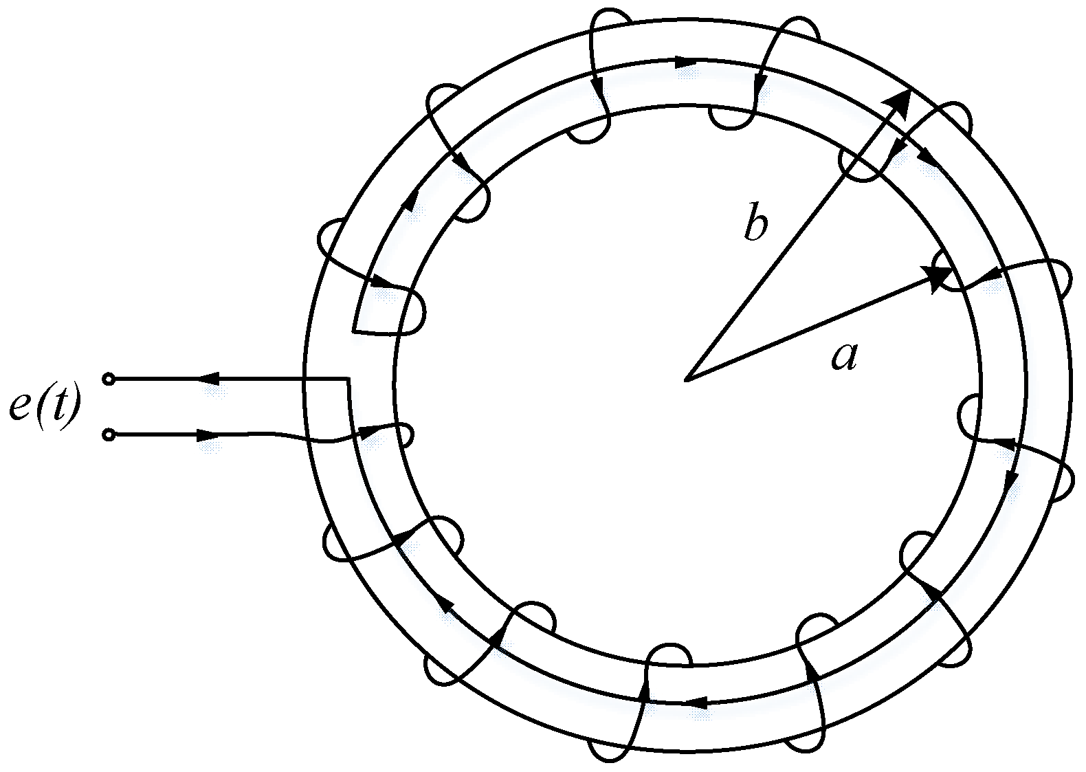
Figure 1. Structure diagram of traditional Rogowski coil.
Electronics 12 01099 g001
Figure 2. PCB Rogowski coil structure. (a) PCB Rogowski 3D structure diagram. (b) PCB Rogowski coil cross-section diagram.
Electronics 12 01099 g002
Figure 3. Lumped parameter model of Rogowski coil.
Electronics 12 01099 g003
Figure 4. PCB Rogowski coil with four different winding methods. (a) Coil 1. (b) Coil 2. (c) Coil 3. (d) Coil 4.
Electronics 12 01099 g004
Figure 5. Differential winding coil structure.
Electronics 12 01099 g005
Figure 6. Enlarged view of differential winding coil structure.
Electronics 12 01099 g006
Figure 7. Influence of single parameter change on mutual inductance. (a) Variation curve of mutual inductance coefficient with outer diameter b. (b) Variation curve of mutual inductance with inner diameter a.
Electronics 12 01099 g007
Figure 8. Size constraint relationship of the differential winding coil.
Electronics 12 01099 g008
Figure 9. Variation curve of coil turns and mutual inductance with inner diameter when the outer diameter of the coil is fixed.
Electronics 12 01099 g009
Figure 10. Physical drawing of coil 1–4.
Electronics 12 01099 g010
Figure 11. Experimental framework [30].
Electronics 12 01099 g011
Figure 12. Bode diagram of coils 1–4 (a) Coil 1. (b) Coil 2. (c) Coil 3. (d) Coil 4.
Electronics 12 01099 g012
Figure 13. Curve fitting and residual diagram of mutual inductance coefficient of coil 1–4 (a) Coil 1. (b) Coil 2. (c) Coil 3. (d) Coil 4.
Electronics 12 01099 g013
Figure 14. Bode diagram of coil 5–7 (a) Coil 5. (b) Coil 6. (c) Coil 7.
Electronics 12 01099 g014
Table 1. Structural parameters of coils 1–4.
Serial NumberInner Radius of Coil a (mm)Outer Radius of Coil b (mm)Through Hole Diameter d1 (mm)Through Hole Pad Diameter d2 (mm)Trace Width dw (mm)Copper Coating Thickness dh (mm)PCB
Thickness d (mm)
Number of Turns N
Coils 118.6410.30.5080.2540.035260
Coils 218.6410.30.5080.2540.035260
Coils 318.6410.30.5080.2540.035260
Coils 418.6410.30.5080.2540.035260
Table 2. Electrical parameters of coils 1–4.
Serial
Number
Mutual Inductance Coefficient M (nH)Inductance Value Lc (μH)Resistance Value
Rc (Ω)
Capacitance Value
Cc (pF)
Coils 118.9691.1382.57524.509
Coils 218.9691.1382.37524.509
Coils 318.9691.1382.37524.509
Coils 418.9691.1382.37524.509
Table 3. Comparison between measured mutual inductance and theoretical values of coils 1–4.
Serial
Number
Coil Mutual Inductance Value M (nH)The Intercept of the Fitted Curve with the Vertical CoordinateExperimentally Obtained Mutual Inductance Values (nH)Error (%)
Coils 118.969−145.78.25696−56.472
Coils 218.969−145.48.54713−54.942
Coils 318.969−141.513.39122−29.406
Coils 418.969−141.213.86182−26.925
Table 4. Bode diagram of coil 5–7.
Serial
Number
Coil Inner
Diameter a (mm)
Coil Outer Diameter b (mm)Through Hole
Diameter d1 (mm)
Through Hole Pad Diameter d2 (mm)The radius of the Outer Circle of the Coil r1 (mm)Trace Width dw (mm)Copper Coating Thickness dh (mm)PCB
Thickness d (mm)
Number of Turns N
Coils 518.6410.30.5080.80.2540.035260
Coils 618.652.60.30.5080.80.2540.035260
Coils 720.6410.30.5080.80.2540.035260
Table 5. Electrical parameters of coil 5–7.
Serial
Number
Coil Mutual
Inductance M (nH)
Coil Inductor Lc (μH)Coil Resistance Rc (Ω)Coil Capacitor Cc (pF)
Coils 518.0891.0852.39322.822
Coils 624.9491.4973.71738.765
Coils 716.5280.9912.15722.431
Table 6. Comparison of mutual inductance coefficient measured by experiment and theoretical value of coil 5–7.
Serial
Number
Theoretical Value
M (nH)
The Intercept of the Fitted Curve with the Vertical CoordinateExperimental Value (nH)Error/%
Coils 518.089−141.812.9366−28.4833
Coils 624.949−137.620.98071−15.9042
Coils 716.528−152.112.49741−24.3418
Disclaimer/Publisher’s Note: The statements, opinions and data contained in all publications are solely those of the individual author(s) and contributor(s) and not of MDPI and/or the editor(s). MDPI and/or the editor(s) disclaim responsibility for any injury to people or property resulting from any ideas, methods, instructions or products referred to in the content.