Article

Gain Enhancement of Microstrip Patch Array Antennas Using Two Metallic Plates for 24 GHz Radar Applications

1
School of Artificial Intelligence, Daegu University, Gyeongsan 38453, Republic of Korea
2
Department of Electronics Engineering, Dongseo University, Busan 47011, Republic of Korea
*
Author to whom correspondence should be addressed.
Electronics 2023, 12(7), 1512; https://doi.org/10.3390/electronics12071512
Submission received: 27 February 2023 / Revised: 22 March 2023 / Accepted: 22 March 2023 / Published: 23 March 2023
(This article belongs to the Special Issue Antenna Designs for 5G/IoT and Space Applications, 2nd Edition)

Abstract

:
In this paper, a method of enhancing gain in a microstrip patch array antenna using two metallic plates for 24 GHz radar applications is presented. A 4 × 1 linear microstrip square patch array antenna covering the 24.0 to 24.25 GHz frequency range and using a shunt-connected series feed network with a tapered power distribution was first designed with a measured maximum gain of 9.8 dBi and dimensions of 30 mm × 12 mm. Two metallic plates were appended along the array axis of the antenna to double the gain in the 4 × 1 array antenna. Effects on performance from varying the tilting angle and length of the metallic plates, such as the input reflection coefficient, the radiation patterns, and gain, were investigated through simulation. Gain enhancement in the 4 × 1 patch array antenna with metallic plates was highest when the tilting angle was around 70°, and gain kept increasing as the length of the metallic plates increased. A prototype of the 4 × 1 patch array antenna was fabricated with plates at a tilting angle of 70°, a length of 50 mm, and a measured maximum gain of 16.8 dBi. Therefore, a gain enhancement of about 7 dB was achieved by adding the metallic plates along the array axis of the 4 × 1 patch array antenna.

1. Introduction

Radar measures the distance, direction, angle, and speed of an object or a target by using reflected electromagnetic waves that return from the object after transmitting them [1]. Radar was developed during World War II for air defense applications to detect German aircraft. Its usage has progressively widened to civilian and commercial applications, such as airports and harbor traffic control, weather forecasting, and Earth remote sensing [2]. Recently, it has been widely used for automotive and industrial applications, such as collision avoidance and adaptive cruise control in advanced cars, for traffic monitoring, level sensing, and motion detection because of low-cost single-chip solutions from semiconductor integration [3].
Radar, in general, is divided into continuous-wave (CW) radar and pulse radar based on the waveform of the transmitted signals [4]. Pulse radar transmits and receives a pulse signal; the shorter the pulse width, the better the distance resolution. Since pulse radar uses pulse waveforms, it has high instantaneous power and requires a wide frequency bandwidth. Therefore, it is challenging to implement in hardware, expensive, and mainly used for military purposes. CW radar is divided into three types: single-tone CW, frequency shift keying (FSK), and frequency-modulated CW (FMCW). In single-tone CW, the object’s speed can be detected by the frequency change due to the Doppler from the object’s movement, when the object reflects the electromagnetic wave. However, this type of radar cannot measure the distance to the object or the velocity of a stationary object. FSK can measure the speed and distance of a moving object by using two or more discrete transmission frequencies but cannot measure the distance to a stationary object. FMCW uses a voltage-controlled oscillator (VCO) to calculate the shift between the received frequency and the transmitted frequency using the linear frequency modulated transmitted frequency to measure the speed and distance of a moving object as well as the distance to a stationary object. Hence, FMCW is the most accurate and widely used method because of its advantages.
Three main operating frequency bands exist for automotive millimeter-wave radar: 24 GHz, 77 GHz, and 79 GHz [5]. The 24 GHz frequency band (24.0 GHz to 24.25 GHz) is allocated to short-ranges up to 30 m and is used in blind-spot detection, rear cross-traffic alerts, and collision avoidance, whereas the 77 GHz frequency band (76 GHz to 77 GHz) is allocated to long ranges up to 250 m and is used in adaptive cruise control and forward collision warning systems. The 79 GHz frequency band (77 GHz to 81 GHz) is allocated to high-resolution short-range applications. The upper millimeter wave band (100 GHz to 300 GHz) or the sub-terahertz band (100 GHz to 1000 GHz) is expected to be used for higher-resolution radar applications shortly [6,7].
A radar system usually consists of transmitter circuitry producing high-frequency signals, a transmitting antenna sending the signals toward the target, a receiving antenna capturing the signal reflected from the target, and a receiver circuitry extracting the information of interest from the received signal [4]. High-gain directional antennas are required for radar systems. Generally, the antennas used for radar systems can be classified into reflector antennas, lens antennas, and array antennas [8,9]. Reflector antennas consist of a feed antenna and a parabolic reflector. The feed antenna, placed at the reflector’s focal point, is the source of the transmitted waves and is the collection point for the received waves. The reflector reflects the transmitted waves in the direction of its axis to make plane waves and reflects the received waves coming from the axis direction to the focal point. Types of reflector antennas used for radar systems are the parabolic reflector antenna, the Cassegrain reflector antenna with dual reflectors, and the offset feed reflector antenna. Lens antennas have been used for radar systems because they can convert a spherical wave into a plane wave to produce high gain. A convex-plane lens using low-loss dielectric material with a relative permittivity greater than 1 can be used. A Luneburg lens, a spherical dielectric lens with a graded index of refraction (increasing toward the center), can create multiple beams using multiple feed antennas. Lens antennas offer several advantages, such as a wide scan angle, a very low sidelobe, and low feed blockage, compared to reflector antennas. Still, they are very thick and heavy at microwave frequencies, and the attenuation caused by the loss tangent of the dielectric material is significant. Various array antennas using different array elements, such as dipoles, waveguide slots, horns, and microstrip patches, have also been widely used to achieve high gain for radar systems. Various planar microstrip patch array antennas are mainly used for commercial semiconductor-integrated radar sensors.
The microstrip patch array antenna configurations are based on the feed network [10,11]. There are three types of feed networks for the microstrip patch array antennas: series, parallel (or corporate), and series-parallel combination. In the parallel feed network, input power is distributed to all radiating elements using power dividers. Larger frequency bandwidths can be achieved, and the configuration is modular. Since the path length to each array element is the same, each element has the same power and phase. However, the parallel feed network requires a very large space; a long length in the feed network causes high feed losses, and discontinuity between line corners causes large mutual coupling effects that distort the radiation patterns resulting in a high cross-polarization level. In the series feed network, array elements are serially fed from a single transmission line, and the total lengths of the feed line can be minimized with reduced losses and lower sidelobes. The series feed network can be divided into in-line and shunt-connected. For the in-line series feed network, array elements are placed in series and are connected by an intervening transmission line. Therefore, it is most compact in size and efficient in space usage. For the connection between array elements, direct connection or coupled connection can be employed. Since the electrical length of the transmission line between the elements changes as the frequency changes, the main beam direction changes and can be used for frequency beam scanning. In addition, the frequency bandwidth of the in-line series feed network is narrower, compared to the corporate network. The shunt-connected series feed network is the same as the in-line series feed network, but the array elements branch out from the transmission line, and each element has only one transmission line. The lengths of the paths between the elements can be adjusted to make the array insensitive to frequency variation. The series-parallel combination feed network can compensate for the disadvantages of series and parallel feed networks.
According to the radar equation, maximum detection range varies as a square root of the antenna gain. Therefore, we can double the maximum detection range by increasing the antenna gain by four times (6 dB) [8]. Various gain enhancement methods for microstrip patch antennas have been attempted. Fabry–Perot cavity (FPC) antennas, formed by the ground plane of the feed patch antenna and a partially reflective surface (PRS) located above the ground plane with some spacing, have been extensively studied for gain enhancement [12,13,14,15,16]. The PRS is also called the superstrate, and it consists of arrays of periodic metallo-dielectric or pure dielectric elements. Gain in the FPC antenna is proportional to the reflection magnitude and the dimensions of the PRS. Hemispherical, extended hemispherical with a cylinder, elliptical, or planar graded index dielectric lenses have been used for gain enhancement [17,18,19,20]. Another method to increase gain is the use of a metallic horn structure mounted on the surface of the patch radiator [21,22,23,24,25]. Gain from the antennas integrated with a surface-mounted horn structure depends on the dimensions and slant angle. For the horn structure, a pyramidal horn, a conical horn, or two side wings can be used.
In this paper, a gain-enhanced 4 × 1 microstrip patch array antenna with metallic plates for 24 GHz radar applications is proposed. First, a reference 4 × 1 microstrip square patch array antenna with a shunt-connected series feed network using a tapered power distribution was designed to cover the 24.0 to 24.25 GHz frequency range. As the tilting angle and length of the metallic plates were varied, variations in the input reflection coefficient (S11), radiation patterns, and gain characteristics of the microstrip patch array antenna with the metallic plates were investigated in order to find the optimum design parameters for gain enhancement. Full-wave simulations were performed using CST Studio Suite (Dassault Systèmes Co., Vélizy-Villacoublay, France) [26].

2. Designing the 4 × 1 Microstrip Square Patch Array Antenna

2.1. The Single Microstrip Square Patch Antenna

First, an inset-fed microstrip square patch antenna to be used as an element of the 4 × 1 microstrip patch array antenna was designed to cover the 24.0 to 24.25 GHz frequency range on an HF-350F substrate (εr = 3.5, h = 0.254 mm, tan δ = 0.0029), as shown in Figure 1a. Initially, the length of square patch antenna was calculated as follows [27]:
L 1 = 0.48 λ g
λ g = c f r ε reff
ε reff = ( ε r + 1 ) 2 + ( ε r 1 ) 2 1 + ( 12 h ) W
W = c 2 f r ε r + 1 2
in which L1 is the side length of the square patch antenna; λg is the guided or effective wavelength considering the relative permittivity of the substrate; fr is the desired resonant frequency of the square patch antenna; c is the speed of light; εr is the relative permittivity of the substrate; εreff is the effective relative permittivity; h is the substrate thickness; and W is the width of the microstrip line.
The calculated length of the square patch using Equations (1) to (4) is L1,calculated = 3.34 mm. By using this information, the length of the inset-fed square patch was then adjusted through simulation by varying the width and length of the inset in order to make the patch resonate at 24.125 GHz, as shown in Figure 1b. The final length of the square patch was L1 = 3.22 mm. For the simulation, the length of the square ground plane was set at Lg1 = Wg1 = 7 mm, and a 100 Ω microstrip feed line with a width of wf1 = 0.125 mm was used. The final width and length of the inset were wis1 = 0.25 mm and lis1 = 1.0 mm, respectively. The simulated frequency bandwidth for a voltage standing wave ratio (VSWR) less than 2 in the input reflection coefficient was 23.853 to 24.404 GHz (2.28%), which covers the 24.0 to 24.25 GHz frequency band.
Simulated realized gain in the +z-axis main lobe direction as a function of frequency and radiation pattern at 24.125 GHz are plotted in Figure 1c,d, respectively. Gain in the 24.0 to 24.25 GHz band ranged from 6.18 dBi to 6.26 dBi with maximum gain at 24.125 GHz. Half power beam width (HPBW) for the y–z plane was 88.7 degrees, whereas for the z–x plane, it was 85.3 degrees.

2.2. Designing 4 × 1 Shunt-Connected Series Feed Networks Using Uniform and Tapered Power Distributions

In this subsection, 4 × 1 shunt-connected series feed networks using uniform and tapered power distributions are designed, and theoretical and simulated scattering parameters of the networks are compared.

2.2.1. Uniform Power Distribution

Figure 2 shows the geometry and scattering parameter characteristics of the 4 × 1 shunt-connected series feed network using a uniform power distribution. Port 1 is connected by a 50 Ω subminiature version A (SMA) connector for measurement, and the characteristic impedance, length, and width of the microstrip line connected to port 1 are Zc1 = 50 Ω, l1 = 1.87 mm, and w1 = 0.54 mm, respectively. Port 1 feeds ports 2 to 5 where four inset-fed square patches are connected. The input impedance of ports 2 to 5 was set to 100 Ω, with the characteristic impedance and width of the microstrip line connected to ports 2 to 5 at Zc2 = 100 Ω and w2 = 0.125 mm, respectively. The spacing among ports 2 to 5 was set to l2 = 7.49 mm, which is about one guided wavelength of the microstrip line at 24.125 GHz. If the power loss in the microstrip line is ignored, the input power to port 1 is the sum of the power delivered to ports 2 to 5:
P 1 = P 2 + P 3 + P 4 + P 5
where P1, P2, P3, P4, and P5 denote the power delivered to ports 1, 2, 3, 4, and 5, respectively.
Port 1 is located between ports 3 and 4, and two 100 Ω microstrip lines branch out to the left and right symmetrically at the end of the 50 Ω microstrip line connected to port 1. Two T-junction structures connect the two branched microstrip lines to ports 2 to 5. A quarter-wavelength transformer (QWT) is used at the input microstrip line of the T-junction structure for impedance matching. For instance, since the characteristic impedance of the microstrip lines to ports 4 and 5 is Zc2 = 100 Ω, the impedance seen at the junction of the microstrip lines toward ports 4 and 5 is Zi1 = Zc2//Zc2 = 50 Ω, which is the parallel impedance of the characteristic impedance of the microstrip lines to ports 4 and 5. Therefore, the impedance of the QWT can be calculated as follows:
Z c 3 = Z c 2 × Z il = 100 × 50 = 70.71   Ω
The corresponding length and width of the QWT are l1 = (1/4 × l2) = 1.87 mm and w3 = 0.29 mm, respectively.
For uniform power distribution, the input power at port 1 is delivered equally to ports 2 to 5. Therefore, the power distribution among ports 2 to 5 is 1:1:1:1, and the power delivered to ports 2 to 5 is one quarter of P1 or P2 = P3 = P4 = P5 = (1/4 × P1). Since the power at a port is proportional to the square of the voltage, and scattering parameters are defined as the input–output voltage ratio between ports, the scattering parameters between port 1 (input) and ports 2 to 5 (output) should theoretically be S21 = S31 = S41 = S51 = 1/2 = −6 dB. The 4 × 1 shunt-connected series feed network with uniform power distribution in Figure 2a was simulated using CST Studio Suite, and the simulated scattering parameters between port 1 (input) and ports 2 to 5 (output) at 24.125 GHz were S21 = S51 = −6.13 dB, S31 = S41 = −5.96 dB, respectively. The simulated scattering parameters at 24.125 GHz were close to −6 dB, and this validates the uniform power delivery from port 1 to ports 2 to 5.

2.2.2. Tapered Power Distribution

To reduce sidelobe levels in the radiation patterns of the 4 × 1 array antenna, a 4 × 1 shunt-connected series feed network using a tapered power distribution ratio of 1:5:5:1 was designed, and the geometry and scattering parameter characteristics are shown in Figure 3. In this case, the characteristic impedance, length, and width of the microstrip line connected to port 1 are Zc1 = 50 Ω, l1 = 1.87 mm, and w1 = 0.54 mm, respectively. Similarly, the input impedance of ports 2 to 5 was set to 100 Ω with the characteristic impedance and width of the microstrip line connected to ports 2 to 5 at Zc2 = 100 Ω and w2 = 0.125 mm, respectively. For a tapered power distribution with a power ratio of 1:5:5:1, the power delivered to the two center ports (3 and 4) is five times that delivered to edge ports (2 and 5). Therefore, the power delivered to center ports 3 and 4 is P3 = P4 = (5/12 × P1), whereas the power delivered to edge ports 2 and 5 is P2 = P5 = (1/12 × P1).
Two QWTs were used for impedance matching: one at the input microstrip line of the T-junction structure, and the other in the middle of the microstrip line of edge ports 2 and 5. For QWT 1 at the input microstrip line of the T-junction structure, different power distributions connected to the input microstrip line need to be considered. For instance, since the power delivered to port 4 (P4) is five times the power delivered to port 5 (P5), and the power ratio of the microstrip line is inversely proportional to the impedance ratio, the impedance of port 5 (Zp5) should be five times the impedance of port 4 (Zp4). If we assume the impedance of port 4 as Zc2 = 100 Ω, the impedance toward port 5 should Zp5 = 5 × Zc2 = 500 Ω. The input impedance at the junction of the microstrip lines toward ports 4 and 5 was Zi1 = Zc2//Zp5 = 83.33 Ω. Therefore, the characteristic impedance of the QWT 1 can be calculated as follows:
Z c 3 = Z c 2 × Z il = 100 × 83.33 = 91.29   Ω
The length and width of QWT 1 are l1 = 1.87 mm and w3 = 0.16 mm, respectively.
For QWT 2 in the middle of the microstrip line of edge ports 2 and 5, impedance transformation of Zp5 (=500 Ω) to Zc2 (=100 Ω) needs to be considered. For example, if a QWT is directly used to transform Zp5 = 500 Ω to Zc2 = 100 Ω, the impedance of the QWT became 223.61 Ω, where the corresponding microstrip line width is extremely small and hard to implement. To avoid this problem, a 100 Ω microstrip line with a quarter-wavelength was located first, followed by the QWT. In this case, the impedance seen at the input of the QWT 2 becomes:
Z i 2 = Z c 2 2 Z p 5 = 100 2 500 = 20   Ω
Therefore, the impedance of QWT 2 can be calculated as follows:
Z c 4 = Z c 2 × Z i 2 = 100 × 20 = 44.72   Ω
The corresponding length and width of QWT 2 are l1 = 1.87 mm and w4 = 0.65 mm, respectively.
For tapered power distribution with a power ratio of 1:5:5:1, the scattering parameter between port 1 (input) and ports 2 and 5 (output) is theoretically S21 = S51 = 1 / 12 = −10.79 dB, whereas the scattering parameter between port 1 (input) and ports 3 and 4 (output) is S31 = S41 = 5 / 12 = −3.8 dB. The 4 × 1 shunt-connected series feed network with a tapered power distribution of 1:5:5:1 in Figure 3a was simulated using CST Studio Suite. The simulated scattering parameters between port 1 (input) and ports 2 and 5 (output) at 24.125 GHz were S21 = S51 = −10.79 dB, whereas the simulated scattering parameters between port 1 (input) and ports 3 and 4 (output) at 24.125 GHz were S31 = S41 = −3.88 dB. The simulated scattering parameters at 24.125 GHz are close to the theoretical scattering parameters, and this validates the tapered power delivery from port 1 to ports 2 to 5.

2.3. Performance of the 4 × 1 Microstrip Square Patch Array Antenna Combined with Shunt-Connected Series Feed Networks Using Uniform and Tapered Power Distributions

This subsection compares the performance of the 4 × 1 microstrip square patch array antenna when combined with shunt-connected series feed networks using uniform and tapered power distributions.
First, the 4 × 1 microstrip square patch array antenna combined with a shunt-connected series feed network using a uniform power distribution was designed by adding four square patches at ports 2 to 5 from Figure 2a, as shown in Figure 4a.
Note that the location of port 1 is between ports 3 and 4 to reduce the size of the array antenna, compared to Figure 2a, and a circular disk was appended to port 1 for impedance matching with a coaxial feed to the SMA connector. The final radius of the circular disk was r1 = 0.45 mm. The width and length of the inset in the patch are wis2 = 0.25 mm and lis1 = 1.1 mm, respectively. The width and length of the ground plane were set at Wg2 = 30 mm and Lg2 = 12 mm, respectively. The values of other parameters were the same as those in Figure 2a. Figure 4b shows the electric field distribution of the 4 × 1 microstrip square patch array antenna combined with the shunt-connected series feed network using uniform power distribution at 24.125 GHz. We observed that the electric fields were almost equally distributed on the four patches corresponding to the uniform power distribution.
Next, the 4 × 1 microstrip square patch array antenna combined with a shunt-connected series feed network using a tapered power distribution ratio of 1:5:5:1 was designed by adding four square patches at ports 2 to 5 from Figure 3a, as shown in Figure 5a. The parameter values are the same as those in Figure 3a and Figure 4a. Figure 5b shows the electric field distribution of the 4 × 1 microstrip square patch array antenna combined with the shunt-connected series feed network using tapered power distribution at 24.125 GHz. The electric fields on the two center patches were much higher than those on the two edge patches, which confirmed the tapered power distribution.
Figure 6 compares performance characteristics such as input reflection coefficient, realized gain in the +z-axis main lobe direction, and the radiation patterns of the 4 × 1 microstrip square patch array antennas combined with the shunt-connected series feed networks using uniform and tapered power distributions. For the 4 × 1 patch array antenna using uniform power distribution, the simulated frequency bandwidth for a VSWR less than 2 in the input reflection coefficient was 23.805 to 24.429 GHz (2.59%), which is slightly larger than that of the single patch antenna. The frequency bandwidth for a VSWR less than 2 in the 4 × 1 patch array antenna using the tapered power distribution was 23.836 to 24.402 GHz (2.35%), which is slightly less than the uniform power distribution. Realized gain in the +z-axis direction of the antenna using uniform power distribution ranged from 11.44 dBi to 11.64 dBi in the 24.0 to 24.25 GHz band with maximum gain at 24.125 GHz, whereas it ranged from 10.94 dBi to 11.11 dBi in the 24.0 to 24.25 GHz band with maximum gain at 24.125 GHz in the 4 × 1 patch array antenna using the tapered power distribution. Therefore, maximum gain at 24.125 GHz was decreased by 0.53 dB when the tapered power distribution was employed instead of the uniform power distribution. For the 4 × 1 patch array antenna using uniform power distribution, HPBW for the y–z plane was 76.7 degrees at 24.125 GHz, whereas for the z–x plane, it was 22.0 degrees with a sidelobe level of −13.4 dB.
For the 4 × 1 patch array antenna using a tapered power distribution, the HPBW for the y–z plane was 75.5 degrees at 24.125 GHz, whereas for the z–x plane, it was 26.6 degrees with a side-lobe level of −21.3 dB. We observed that although the HPBW for the z–x plane increased by 4.6 degrees with a resulting maximum gain reduction, the sidelobe level for the z–x plane decreased by 7.9 dB when the tapered power distribution was used instead of the uniform power distribution.

3. Design of 4 × 1 Microstrip Square Patch Array Antenna Appended with Two Metallic Plates

3.1. Effects from the Tilting Angle when the Metallic Plate Length Is 10 mm

To increase gain in the 4 × 1 patch array antenna using tapered power distribution, two metallic plates were appended along the array axis (x-axis), as shown in Figure 7a. The width of the metallic plates, wm, is the same as the ground plane width of the 4 × 1 patch array antenna. The effects on performance from varying tilting angle θ of the metallic plates were investigated. In this case, the tilting angle was varied from 0° to 90° at increments of 10° when the length of the metallic plates was fixed at lm = 10 mm. Figure 7b,c shows the input reflection coefficients, and the frequencies and magnitudes at the minimum of the input reflection coefficients. The minimum frequency of the input reflection coefficients decreased from 24.106 GHz to 24.02 GHz as θ increased from 0° to 60°. When θ increased to 70° and 80°, the minimum frequency increased to 24.072 GHz and 24.164 GHz, respectively. The minimum frequency decreased to 23.918 GHz when θ increased to 90°. The magnitude at the minimum frequency ranged from −24.59 dB to −33.52 dB except for θ = 60° and 90°. For θ = 60°, the value decreased to −51.08 dB, whereas it increased to −16.66 dB for θ = 90°. Figure 7d,e shows the realized gain characteristics in the +z-axis direction, and the frequencies and values of maximum gain. The maximum gain frequency ranged from 24.1 GHz to 24.2 GHz when θ ranged from 0° to 80°, whereas it decreased to 23.9 GHz at θ = 90°.
When θ increased from 0° to 30°, the maximum gain value decreased from 10.12 dBi to 4.05 dBi owing to the null on the +z-axis direction. As θ increased from 40° to 70°, the value increased from 8.57 dBi to 13.12 dBi. However, it decreased in the range 11.24 dBi to 11.52 dBi, when θ increased to 80° and 90°. Figure 7f,g compares the radiation patterns on the y–z and z–x planes in the +z-axis direction, whereas Figure 7h,i compares 3D radiation patterns when θ = 30° and θ = 70°, respectively. We observed a null on the +z-axis direction when θ = 30°, and maximum gain was highest when the tilting angle was θ = 70°. Therefore, θ = 70° was chosen for maximum gain enhancement. Note that this tilting angle is similar to that of a standard pyramidal horn antenna.

3.2. Effects from the Length of the Metallic Plates when θ = 70°

Next, the effects on performance from length lm of the metallic plates were investigated, as shown in Figure 8. In this case, the length of the metallic plates was varied from 5 mm to 50 mm in increments of 5 mm when the tilting angle was fixed at θ = 70° for maximum gain enhancement. Figure 8b,c shows the input reflection coefficients, and the frequencies and magnitudes at the minimum of the input reflection coefficients. The minimum frequency of the input reflection coefficients increased from 23.894 GHz to 24.156 GHz as lm increased from 5 mm to 15 mm. When lm increased from 20 mm to 50 mm, the minimum frequency decreased to within the 24.054 GHz to 24.094 GHz range. The magnitude at the minimum frequency ranged from −21.96 dB to −26.08 dB except for lm = 20 mm. For lm = 20 mm, the magnitude increased to −19.6 dB.
Figure 8d,e shows the realized gain characteristics in the +z-axis direction, and the frequencies and values of maximum gain. The maximum gain frequency ranged from 23.9 GHz to 24.1 GHz, whereas the maximum gain value increased gradually from 12.33 dBi to 18.29 dBi. Figure 8h shows the 3D radiation patterns for lm = 50 mm. As mentioned earlier, the maximum detection range can be doubled by increasing antenna gain by four times (6 dB) according to the radar equation. In this work, a 7 dBi gain enhancement was selected to double the maximum detection range in consideration of additional losses and errors occurring during fabrication. Therefore, a metallic plate length of lm = 50 mm was chosen for gain enhancement of more than 7 dBi, compared to the 4 × 1 patch array antenna without the metallic plates where maximum gain was 11.11 dBi.

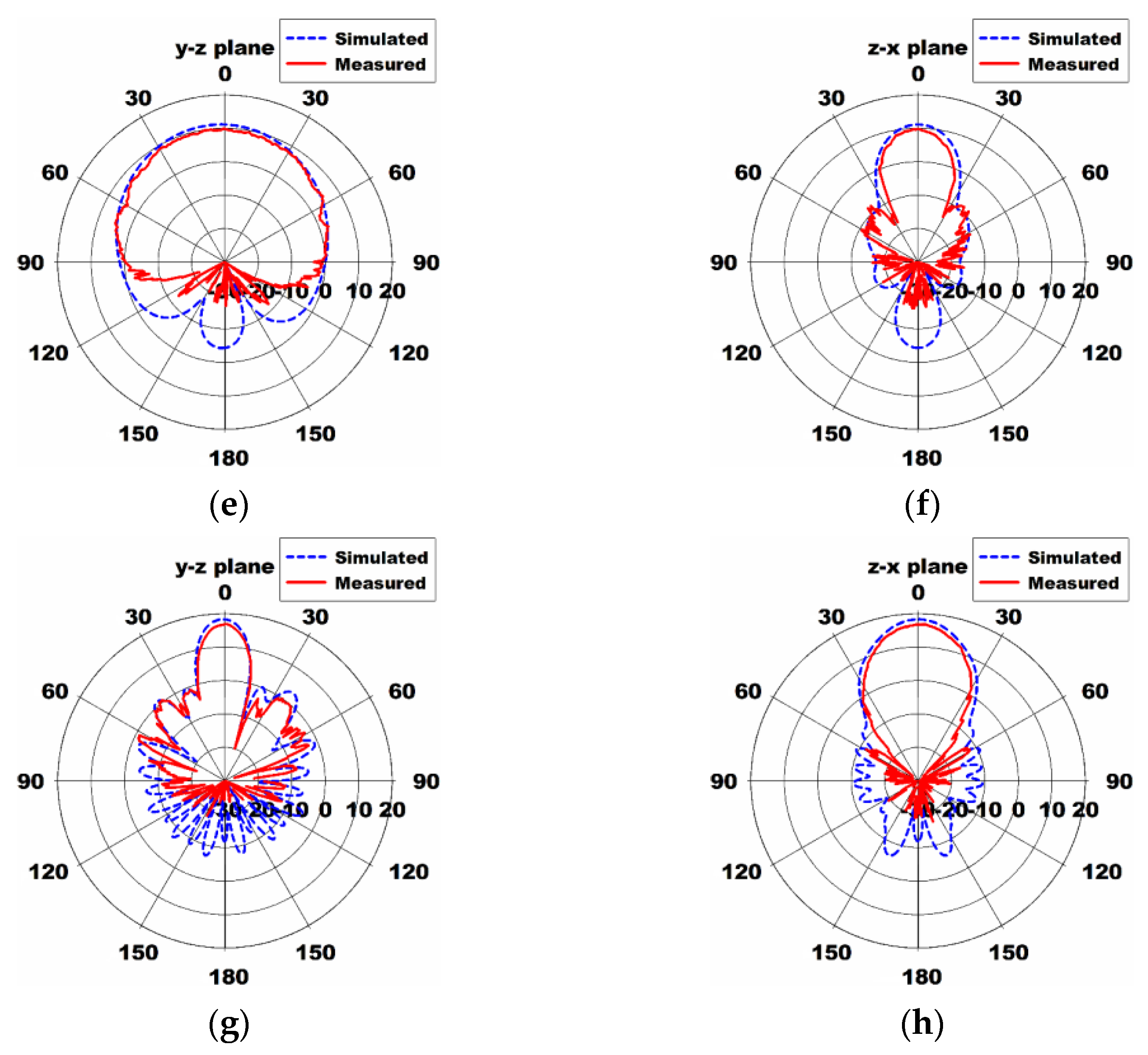
4. Experiment Results and Discussion

To validate the simulated results, the prototypes of the 4 × 1 patch array antennas using uniform and tapered power distributions and the 4 × 1 patch array antenna using a tapered power distribution appended with two metallic plates at the tilting angle θ = 70° and metallic plate length lm = 50 mm were fabricated, as shown in Figure 9. A high-performance SMA connector (PSF-S00-000, GigaLane Co., Ltd., Hwaseong, Korea) designed for applications up to 26.5 GHz, was used. A support structure made of acryl (εr = 2.56) was designed and fabricated using the VLS 3.50 model laser cutting system (Universal Laser Systems, Scottsdale, AZ, USA), as shown in Figure 9c. The dimensions of the support structure are shown in Figure 9d. A 36 μm-thick copper tape (1181, 3M Co., Ltd., Saint Paul, MN, USA) was used to make the two metallic plates.
The simulated and measured results of the fabricated antennas are compared in Figure 10. An Anritsu 37397C vector network analyzer (Anritsu Co., Ltd., Morgan Hill, CA, USA) was used to measure input reflection coefficient and realized gain characteristics. For the 4 × 1 patch array antenna using a uniform power distribution, the simulated and measured frequency bands for a VSWR less than two were 23.805 to 24.429 GHz (2.59%) and 23.851 to 24.840 GHz (4.06%), respectively, and were 23.836–24.402 GHz (2.35%) and 23.819–24.381 GHz (2.33%), respectively, for the 4 × 1 patch array antenna using a tapered power distribution. Note that the measured frequency band for the 4 × 1 patch array antenna using uniform power distribution moved toward a high frequency with a bandwidth increase, whereas the measured frequency band shifted toward a low frequency with a similar bandwidth. For the 4 × 1 patch array antenna using a tapered power distribution appended with two metallic plates, the simulated and measured frequency bands for a VSWR less than two were 23.767 to 24.414 GHz (2.69%) and 23.725 to 24.365 GHz (2.66%), respectively, and, therefore, the measured frequency band shifted toward a low frequency with a similar bandwidth.
For the 4 × 1 patch array antenna using uniform power distribution, the simulated and measured realized gain in the 24.0 to 24.25 GHz band were 11.44 to 11.64 dBi and 10.3 to 10.5 dBi, respectively, with maximum gain decreasing by 1.14 dB. The simulated and measured realized gain in the 24.0 to 24.25 GHz band was 10.94 to 11.11 dBi and 9.7 to 9.8 dBi, respectively, for the 4 × 1 patch array antenna using tapered power distribution, with maximum gain decreasing by 1.31 dB.
For the 4 × 1 patch array antenna using a tapered power distribution appended with two metallic plates, the simulated and measured realized gain in the 24.0 to 24.25 GHz band were 18.19 to 18.29 dBi and 16.7 to 16.8 dBi, respectively, with maximum gain decreasing by 1.49 dB.
The measured radiation patterns of the fabricated antenna on the y–z and z–x planes at 24.125 GHz are compared with the simulated results in Figure 10c–h. The measured radiation patterns agreed quite well with the simulated results. For the 4 × 1 patch array antenna using uniform power distribution, the simulated and measured sidelobe levels for the z–x plane were −13.4 dB and −9.5 dB, respectively, and the measured sidelobe level increased by 3.9 dB. The simulated and measured sidelobe levels for the z–x plane were −21.3 dB and −17.83 dB, respectively, for the 4 × 1 patch array antenna using a tapered power distribution, and the measured sidelobe level increased by 3.47 dB. For the 4 × 1 patch array antenna using a tapered power distribution appended with two metallic plates, the simulated and measured sidelobe levels for the z–x plane were −26.65 dB and −33.66 dB, respectively, and the sidelobe level decreased by 7.01 dB. For the y–z pane, the simulated and measured sidelobe levels were −15.04 dB and −16.17 dB, respectively, and the sidelobe level decreased by 1.13 dB. Note that the sidelobe levels for both the y–z and z–x planes were decreased by appending the two metallic plates.
Table 1 compares the dimensions and performance of the proposed 4 × 1 patch array antenna using a tapered power distribution appended with two metallic plates with other antennas in the literature. Electrical dimensions of the antennas were calculated using the freespace wavelength of the center frequency for the antennas. We can see that the volume of the proposed antenna is the smallest among the antennas in Table 1.

5. Conclusions

We proposed a simple method of enhancing gain in a linear microstrip patch array antenna by appending two metallic plates on the array axis along with adjustment of the tilting angle and the length of the metallic plates for 24 GHz radar applications. First, an inset-fed microstrip square patch antenna with a 100 Ω microstrip feed line, which is used as an element for a 4 × 1 microstrip patch array antenna, was designed to cover the 24.0–24.25 GHz frequency range on an HF-350F substrate.
Next, 4 × 1 shunt-connected series feed networks using uniform power distribution with a power ratio of 1:1:1:1 and tapered power distribution with a power ratio of 1:5:5:1 were designed. Their performance as a power divider was validated through a comparison of the theoretical and simulated results. The input reflection coefficients, realized gain, and radiation patterns of the 4 × 1 microstrip square patch array antennas combined with shunt-connected series feed networks using uniform and tapered power distributions were compared. Maximum gain of the 4 × 1 array antenna with the tapered power distribution decreased 0.53 dB with an increased HPBW, but the sidelobe level of the z–x plane was reduced by 7.9 dB.
Two metallic plates were appended along the array axis to increase gain in the 4 × 1 patch array antenna using the tapered power distribution. The effects on the array antenna performance from the tilting angle and the length of the metallic plates were investigated. We found that maximum gain was highest when the tilting angle was around 70°, and it increased gradually as the length of the two metallic plates increased. To achieve 7 dB gain enhancement (doubling the maximum detection range), a metallic plate length of 50 mm was selected.
Measured maximum gain of the 4 × 1 patch array antenna using the tapered power distribution without metallic plates was 9.8 dBi at 24.125 GHz, whereas the measured maximum gain of the antenna appended with metallic plates was 16.8 dBi. Therefore, a 7 dB gain enhancement can be achieved by adding two metallic plates along the array axis.
Maximum gain might be slightly enhanced by appending two more metallic plates along the axis perpendicular to the array to surround the whole four sides of the array antenna, but the cost and complexity of the fabrication might be considerably increased.
The proposed method can be applied to various radar and millimeter wave applications. It can also be used for satellite communications and future mobile communication systems (5G and 6G). In future work, we plan to conduct research on the production of integrated antennas by using 3D printers.

Author Contributions

J.Y. contributed the idea, the simulation, the analysis, and the overall research. J.-I.L. contributed fabrications and measurements. All authors have read and agreed to the published version of the manuscript.

Funding

This research was supported by Daegu University Research Grant 2019.

Data Availability Statement

Not applicable.

Conflicts of Interest

The authors declare they have no conflict of interest.

References

  1. Skolnik, F.; Merrill, I. Introduction to Radar: Radar Handbook; McGraw-Hill: New York, NY, USA, 1962. [Google Scholar]
  2. James, R.J. A history of radar. IEE Rev. 1989, 35, 343–349. [Google Scholar] [CrossRef]
  3. Greco, M.S.; Li, J.; Long, T.; Zoubir, A. Advances in radar systems for modern civilian and commercial applications: Part 1 [From the Guest Editors]. IEEE Signal Process. Mag. 2019, 36, 13–15. [Google Scholar] [CrossRef]
  4. Lin, J.; Li, C.; Chang, C.C.; Tsai, T.; Zito, D.; Chang, S.F. Review—Semiconductor integrated radar for sensing applications. ECS J. Solid State Sci. Technol. 2018, 7, 3126–3142. [Google Scholar] [CrossRef]
  5. Chipengo, U.; Krenz, P.M.; Carpenter, S. From antenna design to high fidelity, full physics automotive radar sensor corner case simulation. Model. Simul. Eng. 2018, 2018, 4239725. [Google Scholar] [CrossRef] [Green Version]
  6. Sabery, S.M.; Bystrov, A.; Navarro-Cía, M.; Gardner, P.; Gashinova, M. Study of low terahertz radar signal backscattering for surface identification. Sensors 2021, 21, 2954. [Google Scholar] [CrossRef]
  7. Xiao, L.; Xie, Y.; Gao, S.; Li, J.; Wu, P. Generalized radar range equation applied to the whole field region. Sensors 2022, 22, 4608. [Google Scholar] [CrossRef] [PubMed]
  8. Edde, B. RADAR: Principles, Technology, Applications; Prentice Hall, Inc.: Englewood Cliffs, NJ, USA, 1993. [Google Scholar]
  9. Menzel, W.; Moebius, A. Antenna concepts for millimeter-wave automotive radar sensors. Proc. IEEE 2012, 100, 2372–2379. [Google Scholar] [CrossRef]
  10. Aydemir, A.E. Development of K Band Microstrip Patch Antenna Array for Traffic Radars. Master’s Thesis, Middle East Technical University, Ankara, Turkey, 13 November 2017. [Google Scholar]
  11. Errifi, H.; Baghdad, A.; Badri, A.; Sahel, A. Design and analysis of directive microstrip patch array antennas with series, corporate and series-corporate feed network. Int. J. Electr. Electron. Eng. 2015, 3, 416–423. [Google Scholar] [CrossRef] [Green Version]
  12. Trentini, G.V. Partially reflecting sheet arrays. IRE Trans. Antennas Propag. 1956, 4, 666–671. [Google Scholar] [CrossRef]
  13. Nguyen, T.K.; Park, I. Design of a low-profile, high-gain Fabry-Perot cavity antenna for Ku-band applications. J. Electromagn. Eng. Sci. 2014, 14, 306–313. [Google Scholar] [CrossRef]
  14. Goudarzi, A.; Honari, M.M.; Mirzavand, R. Resonant cavity antennas for 5G communication systems: A review. Electronics 2020, 9, 1080. [Google Scholar] [CrossRef]
  15. Aqlan, B.; Vettikalladi, H.; Alkanhal, M. Millimeter wave antenna with frequency selective surface (FSS) for 79 GHz automotive radar applications. Int. J. Microw. Wirel. Technol. 2017, 9, 281–290. [Google Scholar] [CrossRef]
  16. Yang, X.X.; Tan, G.N.; Han, B.; Xue, H.G. Millimeter wave Fabry-Perot resonator antenna fed by CPW with high gain and broadband. Int. J. Antennas Propag. 2016, 2016, 3032684. [Google Scholar] [CrossRef] [Green Version]
  17. Nguyen, N.T.; Rolland, A.; Boriskin, A.V.; Valerio, G.; Le Coq, L.; Sauleau, R. Size and weight reduction of integrated lens antennas using a cylindrical air cavity. IEEE Trans. Antennas Propag. 2012, 60, 5993–5998. [Google Scholar] [CrossRef]
  18. Malik, B.T.; Doychinov, V.; Zaidi, S.A.R.; Robertson, I.D.; Somjit, N. Antenna gain enhancement by using low-infill 3D-printed dielectric lens antennas. IEEE Access. 2019, 7, 102467–102476. [Google Scholar] [CrossRef]
  19. Ahmad, W.; Dayi, F.; Rehman, H.; Khan, W. Low-cost and small size millimeter wave (24 GHz) extended hemispherical lens antenna for automotive and industrial applications using FR408HR substrate. Prog. Electromagn. Res. Lett. 2021, 100, 73–80. [Google Scholar] [CrossRef]
  20. Poyanco, J.M.; Pizarro, F.; Rajo-Iglesias, E. Cost-effective wideband dielectric planar lens antenna for millimeter wave applications. Sci. Rep. 2022, 12, 4204. [Google Scholar] [CrossRef] [PubMed]
  21. Ranga, Y.; Verma, A.K.; Esselle, K.P.; Weily, A.R. Gain enhancement of UWB slot with the use of surface mounted short horn. In Proceedings of the 2010 IEEE Antennas and Propagation Society International Symposium, Toronto, ON, Canada, 2 September 2010; pp. 1–4. [Google Scholar]
  22. Ononchimeg, S.; Otgonbaatar, G.; Bang, J.H.; Ahn, B.C. A new dual-polarized horn antenna excited by a gap-fed square patch. Prog. Electromagn. Res. Lett. 2011, 21, 129–137. [Google Scholar] [CrossRef] [Green Version]
  23. Sethi, W.H.; Vettikalladi, H.; Alkanhal, M.A. Millimeter wave antenna with mounted horn integrated on FR4 for 60 GHz Gbps communication systems. Int. J. Antennas Propag. 2013, 2013, 834314. [Google Scholar] [CrossRef] [Green Version]
  24. Boas, E.C.V.; Ferrero, M.A.S.; Nasri, A.; Mittra, R.; Sodré, A.C. 31 dBi-gain slotted waveguide antenna array using wing-based reflectors. IEEE Access. 2022, 10, 57327–57338. [Google Scholar] [CrossRef]
  25. Jung, Y.B.; Park, D.Y.; Jung, C.W. Low cost 24GHz patch array antenna for high sensitivity EM sensor. In Proceedings of the 2010 Asia-Pacific Microwave Conference, Yokohama, Japan, 7–10 December 2010; pp. 2208–2211. [Google Scholar]
  26. Electromagnetic Simulation Solvers, CST Studio Suite. Available online: https://www.3ds.com/products-services/simulia/products/cst-studio-suite/solvers/ (accessed on 28 February 2023).
  27. Ahmad, S. A Linear Array Design Based on Non-Uniform Chebyshev Distribution for High Gain Low Sidelobe Level Millimetre Wave 5G Applications. Master’s Thesis, Universitat Politècnica de Catalunya·BarcelonaTech, Barcelona, Spain, 31 August 2020. [Google Scholar]
  28. Rabbani, M.S.; Churm, J.; Feresidis, A.P. Fabry–Perot beam scanning antenna for remote vital sign detection at 60 GHz. IEEE Trans. Antennas Propag. 2021, 69, 3115–3124. [Google Scholar] [CrossRef]
Figure 1. Design and performance of the single microstrip patch antenna: (a) the geometry, (b) the input reflection coefficient, (c) realized gain in the +z-axis direction, and (d) radiation patterns on the y–z and z–x planes at 24.125 GHz.
Electronics 12 01512 g001
Figure 2. Geometry and scattering parameter characteristics of the 4 × 1 shunt-connected series feed network using a uniform power distribution: (a) the geometry and (b) scattering parameters.
Electronics 12 01512 g002
Figure 3. Design and scattering parameter characteristics of the 4 × 1 shunt-connected series feed network using tapered power distribution: (a) the geometry and (b) scattering parameters.
Electronics 12 01512 g003
Figure 4. Design and electric field distribution of the 4 × 1 microstrip square patch array antenna combined with a shunt-connected series feed network using a uniform power distribution: (a) the geometry and (b) the electric field distribution at 24.125 GHz.
Electronics 12 01512 g004
Figure 5. Design and electric field distribution of the 4 × 1 microstrip square patch array antenna combined with a shunt-connected series feed networks using a tapered power distribution: (a) the geometry and (b) the electric field distribution at 24.125 GHz.
Electronics 12 01512 g005
Figure 6. Performance comparison of the 4 × 1 microstrip square patch array antenna combined with shunt-connected series feed networks using uniform and tapered power distributions: (a) the input reflection coefficient, (b) the realized gain in the +z-axis direction, (c) the radiation patterns on the y–z plane at 24.125 GHz, and (d) the radiation patterns on the z–x plane at 24.125 GHz.
Electronics 12 01512 g006
Figure 7. Effects from tilting angle θ of the 4 × 1 array antenna appended with two metallic plates when lm = 10 mm: (a) the geometry, (b) S11, (c) the frequencies and magnitudes at the minimum of S11, (d) realized gain, (e) the frequencies and values of maximum gain, (f) radiation patterns on the y–z plane for maximum gain frequency, (g) radiation patterns on the z–x plane for maximum gain frequency, (h) 3D radiation pattern at θ = 30°, and (i) 3D radiation pattern at θ = 70°.
Electronics 12 01512 g007aElectronics 12 01512 g007b
Figure 8. Effects from length lm of the two metallic plates on the 4 × 1 microstrip square patch array antenna when θ = 70°: (a) the geometry for lm = 50 mm, (b) S11, (c) the frequencies and magnitudes at the minimum of S11, (d) realized gain, (e) the frequencies and values of maximum gain, (f) radiation patterns on the y–z plane at maximum gain frequency, (g) radiation pattern at z–x planes at maximum gain frequency, and (h) the 3D radiation pattern for lm = 50 mm.
Electronics 12 01512 g008aElectronics 12 01512 g008b
Figure 9. Photographs and dimensions of the fabricated antennas: (a) the 4 × 1 array antenna using uniform power distribution, (b) the 4 × 1 array antenna using tapered power distribution, (c) the 4 × 1 array antenna using tapered power distribution with metallic plates, and (d) the dimensions of the acrylic support structure for the metallic plates. (All units are in millimeters).
Electronics 12 01512 g009
Figure 10. Performance comparison of the fabricated antennas: (a) input reflection coefficients, (b) realized gain, (c) y–z plane radiation patterns at 24.125 GHz for the 4 × 1 array antenna using uniform power distribution, (d) z–x plane radiation patterns at 24.125 GHz for the 4 × 1 array antenna using uniform power distribution, (e) y–z plane radiation patterns at 24.125 GHz for the 4 × 1 array antenna using tapered power distribution, (f) z–x plane radiation patterns at 24.125 GHz for the 4 × 1 array antenna using tapered power distribution, (g) y–z plane radiation patterns at 24.125 GHz for the 4 × 1 array antenna using tapered power distribution appended with two metallic plates, and (h) z–x plane radiation patterns at 24.125 GHz for the 4 × 1 array antenna using tapered power distribution appended with two metallic plates.
Electronics 12 01512 g010aElectronics 12 01512 g010b
Table 1. Comparison of dimensions and performance of the proposed antenna with other antennas in the literature.
ReferencesAntenna TypePhysical
Dimensions (mm3)
Electrical
Dimensions (λ03)
Bandwidth (GHz) for VSWR < 2Maximum Gain (dBi)
[19]Patch antenna + Hemispherical lens65 × 60 × 495.18 × 4.78 × 3.90
(96.57 λ03)
23.35–24.45
(fc = 23.9)
15.2
[20]Waveguide antenna + Planar graded index lens89 × 89 × 3210.09 × 10.09 × 3.63
(369.56 λ03)
28.0–40.0
(fc = 34.0)
25.7
[24]27 × 1 slot array antenna + Two wing reflectors260 × 74 × 5422.33 × 6.36 × 4.64
(658.97 λ03)
24.94–26.60
(fc = 25.77)
30.5
[28]2 × 1 series-fed patch array antenna + PRS50 × 30 × 1010.79 × 6.48 × 2.16
(151.03 λ03)
62.5–67.0
(fc = 64.75)
20.1
This Work4 × 1 patch array antenna + Two metallic plates30 × 46.2 × 472.40 × 3.70 × 3.77
(33.48 λ03)
23.35–24.45
(fc = 24.045)
16.8
Disclaimer/Publisher’s Note: The statements, opinions and data contained in all publications are solely those of the individual author(s) and contributor(s) and not of MDPI and/or the editor(s). MDPI and/or the editor(s) disclaim responsibility for any injury to people or property resulting from any ideas, methods, instructions or products referred to in the content.

