Article

Comparative Study of the Parameter Acquisition Methods for the Cauer Thermal Network Model of an IGBT Module

1
Institute of Electronics Packaging Technology and Reliability, Faculty of Materials and Manufacturing, Beijing University of Technology, Beijing 100124, China
2
Beijing Key Laboratory of Advanced Manufacturing Technology, Beijing University of Technology, Beijing 100124, China
*
Author to whom correspondence should be addressed.
Electronics 2023, 12(7), 1650; https://doi.org/10.3390/electronics12071650
Submission received: 10 January 2023 / Revised: 23 March 2023 / Accepted: 27 March 2023 / Published: 31 March 2023

Abstract

:
Under the operating conditions of high power and high switching frequency, an insulated gate bipolar transistor (IGBT) chip can produce relatively large power loss, causing the junction temperature to rise rapidly; consequently, the reliability of the IGBT module can be seriously affected. Therefore, it is necessary to accurately predict the junction temperature of the IGBT chip. The resistance capacitance (RC) thermal network model is a commonly used method for IGBT junction temperature prediction. In this paper, the model parameters are obtained by two methods to establish the Cauer thermal network models of the IGBT module. The first method is to experimentally obtain the transient thermal impedance curve of the IGBT module and the structure function and then extract the individual thermal parameters of the Cauer thermal network model; the second method is to obtain the thermal parameters of the thermal network model directly by using theoretical formulas that consider the influence of the heat spreading angle. The predicted junction temperatures of the Cauer thermal network models established by the two methods are compared with the junction temperatures obtained from infrared (IR) measurements during the power cycling test, the junction temperatures measured by the temperature-sensitive electrical parameter (TSEP) method, and the junction temperatures calculated by finite element (FE) analysis. Additionally, the Cauer thermal network models established by the two methods are compared and verified. The results indicate that the Cauer thermal network model established based on theoretical formulas can accurately predict the maximum junction temperature of the IGBT chip, and the calculated temperature for each layer, from the IGBT chip layer to the ceramic layer, also accords well with the FE results. The Cauer thermal network model established based on the experimental test and the structure function can accurately predict the average junction temperature of the IGBT chip.

1. Introduction

Insulated gate bipolar transistors (IGBTs) have become the most important devices in power electronics applications, such as high-power converters, and their reliability directly determines whether the entire system can operate safely and reliably [1,2]. In the service state, the current and voltage of the IGBT module cyclically fluctuate during the turn-on, on-state, and turn-off processes as the working conditions change, causing changes in the power loss of the IGBT chip. The conduction power loss and switching power loss dissipate and generate large amounts of heat, which will increase the junction temperature of the chip. The average junction temperature in the normal service state can reach 60–80 °C, and the junction temperature swing can reach 70–90 °C or even higher [3]. When the IGBT module is operated under working conditions with large junction temperature fluctuations, each material layer can repeatedly undergo thermal expansion and cooling shrinkage. The coefficient of thermal expansion (CTE) of each layer is different [4], and this thermal mismatch may cause each layer to be repeatedly subjected to thermal stress, causing damage to the material and structure and resulting in degradation in the electrical and heat transfer characteristics of the IGBT module [5], thus eventually leading to bond wire liftoff and solder layer delamination and causing IGBT module failure [6]. Studies have demonstrated that approximately 55% of the failures of electronics are caused by temperature rise [7], and the failure probability of the IGBT module increases sharply with increasing temperature; i.e., for every 10 °C increase in temperature, the failure probability doubles [8]. Because the junction temperature greatly affects the reliability of the IGBT module, accurately predicting the junction temperature of the IGBT module in the service state is of great practical value for ensuring the long-term safe operation of the IGBT module [9].
At present, many advanced methods have been introduced for the junction temperature estimation of the high-power IGBT module. The main experimental methods for obtaining the junction temperature of the IGBT module include optical measurements, physical contact measurements, and temperature-sensitive electrical parameters (TSEPs) [10,11,12,13]. Simulation tools have been applied for thermal behavior analysis of the IGBT module, such as the finite element (FE) method [14,15,16]. FE analyses can obtain the temperature field of the entire IGBT module, but they normally require massive calculations, and it is difficult to be implemented in real mission profiles. FE analyses can obtain the temperature field of the entire IGBT module, but they require a long calculation time. Additionally, resistance capacitance (RC) thermal network models have been widely used for junction temperature calculation of IGBT modules [17]. RC thermal network models are based on thermal–electrical analogy theory; they convert thermal parameters into electrical parameters, integrate the parameters into circuit simulation software, can rapidly calculate IGBT module junction temperatures, and have a wide range of applications [18,19].
The commonly used RC thermal network models include the Foster thermal network model and the Cauer thermal network model. The thermal parameters (thermal resistance and thermal capacitance) of the Foster thermal network model are relatively easy to obtain. The commonly used method is to calculate the transient thermal impedance curve of the IGBT module by using FE analysis and to obtain the thermal parameters of the Foster thermal network model by directly fitting the curve [20,21,22]. In addition, based on the thermal parameters given by the IGBT module supplier, the Foster thermal network model can also be directly established [23]. One shortcoming of the Foster thermal network model is that only the junction temperature and the baseplate temperature can be obtained, whereas the temperature of each material layer within the IGBT module cannot be obtained.
Since the thermal parameters of each layer of the Cauer thermal network model are needed, obtaining the parameters of the Cauer thermal network model is more difficult than obtaining those of the Foster thermal network model. One of the methods currently used is to obtain the thermal resistance and thermal capacitance of each material layer through theoretical calculations based on the geometric dimensions and material parameters of each layer of the IGBT module [24,25]. Some scholars have used this theoretical calculation to obtain parameters to establish a Cauer thermal network model of the press-pack IGBT (PP-IGBT) module and verified the established model by comparing the results with the experimental and FE results [26,27]. In addition, some researchers have obtained the parameters of each layer by analyzing the structure function of the transient thermal impedance curve and established the Cauer thermal network model of the PP-IGBT module [28]. The greatest advantage of the Cauer thermal network model is that the temperature of each material layer of the IGBT module can be obtained.
In this paper, the Cauer thermal network model of the IGBT module is established using two methods: obtaining the model parameters based on the experimentally obtained transient thermal impedance curves and structural functions and obtaining the model parameters based on theoretical calculation. The junction temperatures calculated by the Cauer thermal network models are compared with the junction temperatures obtained from infrared (IR) measurements, the junction temperatures measured by the TSEP method, and the junction temperatures calculated by FE analysis; additionally, the characteristics, advantages, and disadvantages of the two methods of building the Cauer thermal network model are analyzed.

2. IGBT Module Structure and Heat Transfer Process

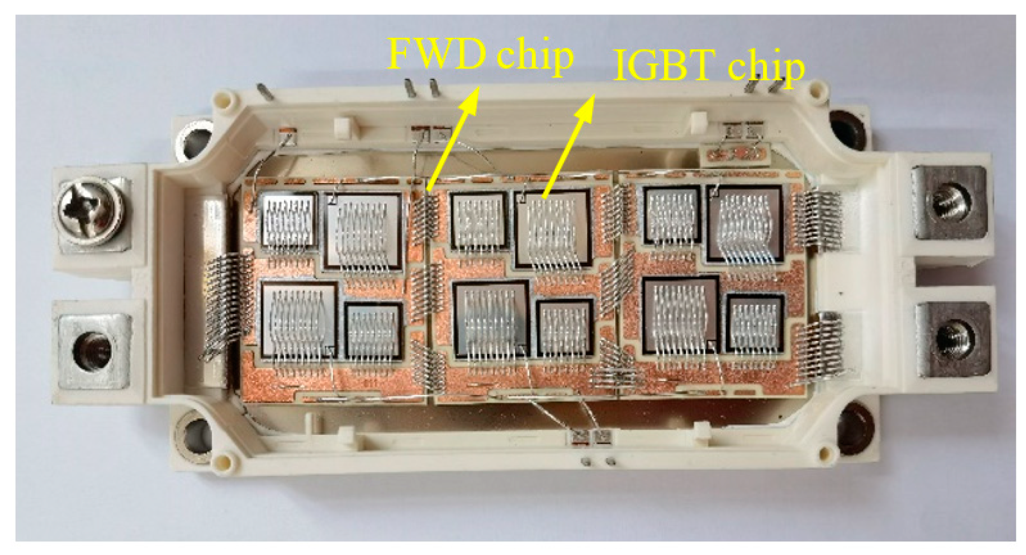
2.1. IGBT Module Structure for the Experiment

As shown in Figure 1, a half-bridge IGBT module with a rated voltage of 1200 V and a rated current of 450 A is selected. An IGBT module contains six IGBT chips and six freewheel diode (FWD) chips and has upper and lower bridge arms. Each bridge arm contains three IGBT chips, and one IGBT chip is connected reverse parallel to one FWD chip. All chips are soldered on three direct bonding copper (DBC) ceramic baseplates, an Al metallization layer is sputtered on the surface of the chip, and electrical interconnection to the upper Cu layer of the DBC is achieved via nine Al bond wires. The DBC is connected to the Cu baseplate through a solder layer. In addition, the IGBT module includes protective structures, such as lead-out terminals, silicone gel, and a baseplate.

2.2. Simplification of the Heat Transfer Process of the IGBT Module

(1)
The heat dissipation process considers the heat conduction process only from the chip to the heat sink.
In the service state, the chips in the IGBT module are the main heat source. For the heat generated in the IGBT module, heat conduction is the main heat transfer mechanism, while after reaching the heat sink, the heat diffuses to the external environment in the forms of thermal convection and thermal radiation, as shown in Figure 2. Since the silicone gel on the upper surface of the IGBT module has a good thermal insulation performance, the convective heat transfer on the surface can be ignored. In addition, the junction temperature of the IGBT module generally does not exceed 150 °C, and the thermal radiation can also be ignored. Therefore, the heat dissipation process of the IGBT module considers the heat conduction process only from the IGBT chip to the heat sink, and the heat dissipation on the module’s surface and side is ignored [18,22].
(2)
The three-dimensional heat conduction problem of the IGBT module is simplified to a one-dimensional heat conduction problem.
To use the lumped-parameter method to simplify the three-dimensional heat conduction problem of the IGBT module to a one-dimensional heat conduction problem, it is necessary to satisfy certain requirements; i.e., the thermal conductivity of the object is large, the surface area is large, the surface convection heat transfer coefficient is very small, the thickness is very low, and the thermal resistance inside the object is negligible compared to the convective heat transfer resistance of the surface. Then, the Biot number, Bi, is introduced:
B i = h l λ < 0.1 M
where h is the convective heat transfer coefficient on the surface of the object, l is the thickness of the object, λ is the thermal conductivity of the object, and M is a constant related to the geometric shape of the object. For infinite flat plates, M = 1; for infinitely long cylinders and square columns, M = 1/2; and for spheres and cubes, M = 1/3. In general, because each layer in the IGBT module is very thin (that is, l is very small), each layer can be regarded as an infinite plate, and M = 1. The convective heat transfer on the surface of the IGBT module can be ignored; consequently, h is small. Therefore, for each layer of the IGBT module, Bi < 0.1, which satisfies the applicable condition of the lumped-parameter method [29], and the one-dimensional heat conduction equation can be used to describe the heat conduction process inside the IGBT module.
(3)
The thermal coupling effect between IGBT chips is ignored.
In the direct current (DC) power cycling test, only the upper half of the IGBT module is connected to the circuit, and the FWD chips do not work; that is, only three IGBT chips work at the same time. The upper copper layer of the IGBT module is three separate pieces of copper instead of one piece of copper. Such structure features will reduce the coupling effect between IGBT chips. Additionally, studies have demonstrated that when the distance between two chips is greater than 10 mm, the thermal coupling effect between them can be ignored [30]. The distance between the IGBT module chips used in this paper is 19 mm; therefore, under the DC power cycling test, the thermal coupling effect between chips can be ignored.
In summary, to calculate the junction temperature of an IGBT chip, only the vertical thermal path must be considered.

3. Modeling Process of the RC Thermal Network Model of the IGBT Module

3.1. Cauer Thermal Network Model Structure

A one-dimensional Cauer thermal network model for the IGBT module is established, as shown in Figure 3. The established RC thermal network model has a heat flow path, which contains seven RC units, corresponding to the IGBT module’s seven-layer structure, consisting of the IGBT chip, the chip solder layer, the upper Cu layer of the DBC, the ceramic layer of the DBC, the lower Cu layer of the DBC, the DBC solder layer, and the Cu baseplate layer. The Cauer thermal network model contains RC units, which are corresponding to the IGBT module’s material layers, and thus, the temperature of all the material layers within the IGBT module can be obtained. Here, to obtain the temperature results of some material layers that cannot be obtained, the order reduction techniques were not applied [31]. In the thermal–electrical analogy method, the heat transfer process in the IGBT module is analogous to the electrical conduction process by treating temperature T, heat flow P, thermal resistance Rth, and thermal capacitance Cth as voltage U, current I, resistance Rel, and capacitance Cel, respectively. An equivalent circuit model is established in the circuit simulation software to analyze the thermal conduction characteristics of the IGBT module, and the obtained node voltage between each RC unit is the temperature of each layer.

3.2. Determining the Parameters of the RC Thermal Network Model by Using the Transient Thermal Impedance Curve Test and Structure Function

First, the K curve is obtained through experiments. Before the experiment, a calibration test is performed to obtain the relationship between the on-state collector–emitter voltage drop (Vce-on) and the junction temperature (Tj), i.e., the K curve. A thermostat experimental device is used to obtain the Vce-on of the device under test (DUT) under different Tjs, the curve of Tj and Vce-on is plotted, and the K curve is obtained by fitting the data. The results are shown in Figure 4, and the K factor of the IGBT module is −2.35 mV/°C.
Then, the T3Ster thermal resistance tester is used to measure the transient thermal impedance curve of the IGBT module. The configuration of the transient thermal impedance curve measurement is shown in Figure 5. When the transient thermal impedance curve test starts, a heating current of 100 A flows through the DUT for a heating time of 200 s. The IGBT module is heated to thermal equilibrium, the heating current is turned off, and water cooling is started. At this time, the test current is applied to the circuit to measure the Vce-on of the DUT in the cooling stage, and the sampling interval is 1 μs. The Tj(t) during the cooling process is calculated using the K curve. Then, from the Tj(t) and the heating power P, the transient thermal impedance curve Zth, cooling(t) during the cooling process can be obtained, as shown in Figure 6.
Z th , cooling t = T j t T j t = 0 P
The cumulative structure function C(Rth) and differential structure function ρ(Rth) are obtained by mathematical transformations of the transient thermal impedance curve, such as numerical derivation and deconvolution.
C R th = c ρ λ A 2 R th
ρ R th = d C R th R th = c ρ λ A 2
where Rth is the thermal resistance, c is the specific heat capacity of the material, ρ is the material density, λ is the thermal conductivity of the material, and A is the effective heat transfer area.
The cumulative structure function and the differential structure function can provide the thermal resistances and thermal capacitances of the material layers within the IGBT module. According to the cumulative structure function (Equation (3)), when the heat transfer area of a certain material layer changes or the heat enters one material layer from another material layer, the slope of the cumulative structure function curve may change. As shown in Equation (4), the differential structure function is the derivative of the cumulative structure function on the thermal resistance; that is, at the same position, the change in the slope of the cumulative structure function curve could lead to the extreme value of the differential structure function curve. According to this feature, the thermal resistance and thermal capacitance of each material layer can be determined by dividing the cumulative and differential structure function curves. Figure 7 shows the cumulative structure function and differential structure function curves of the IGBT module. Based on the structure function, the thermal resistance Rth and the thermal capacitance Cth of each material layer of the tested IGBT module are obtained, as shown in Table 1.

3.3. Determining the Parameters of the RC Thermal Network Model by Using Theoretical Formulas

The thermal resistance Rth and the thermal capacitance Cth of each layer can be calculated according to the following equation:
R th = l λ A
C th = c ρ A l
where λ is the thermal conductivity of each material layer, A is the effective heat transfer area of each layer, c is the specific heat capacity of each layer, ρ is the density of each layer, and l is the thickness of each layer. The effective heat conduction area A is one of the key factors affecting the thermal resistance and thermal capacitance of each layer.
In the IGBT module, the heat generated by the IGBT chip not only diffuses in the vertical direction but also laterally diffuses when the area of the heat source is small; that is, the effective heat conduction area can gradually expand [32,33], as shown in Figure 8. Here, it is assumed that the heat source is a square, where Lh is the 1/2 side length of the heat source, Ls is the 1/2 side length of the layer for determining the thermal capacitance and thermal resistance, l is the thickness of the layer, and θ is the heat spreading angle (0 < θ < 90°). When calculating the effective heat transfer area, the two cases of l ≤ (LsLh)/tanθ and l > (LsLh)/tanθ must be considered. As shown in Figure 8a,b, the effective heat conduction area at any point x in the coordinate system is
A x = 4 L h + x tan θ 2               x l L s L h tan θ A x = 4 L s 2                                   L s L h tan θ < x l
Substituting Equation (7) into Equations (5) and (6) and integrating along the thickness of the layer, we have
R th = 0 L s L h tan θ d x 4 λ L h + x tan θ 2 + L s L h tan θ l d x 4 λ L s 2         = 1 4 λ L h l L h + l tan θ + L h l l L s 2   C th = 0 L s L h tan θ 4 c ρ L h + x tan θ 2 d x   + L s L h tan θ l 4 c ρ L s 2 d x        =     4 c ρ 3 tan θ L h + l tan θ 3 L h 3 + 4 c ρ L s 2 l l
where the equivalent thickness l* is [34]
l = min L s L h tan θ ,    l
Equation (8) indicates that the key to calculating the thermal resistance and thermal capacitance is the heat spreading angle. Existing studies take the heat spreading angle as a certain value, such as 45° [35], 32.5° [36], and 26.6° [37], which can meet the requirement when the computational accuracy is low. However, to obtain a more accurate thermal resistance and thermal capacitance, it is necessary to further consider the influence of the lateral boundary effect and the vertical boundary effect on the heat spreading angle.
First, the influence of the lateral boundary effect on the heat spreading angle is analyzed; this influence refers mainly to the influence of the lateral dimension of the layer. In Figure 9a, when Lh/Ls << 1, the area of the heat source is much smaller than the area of the layer, and the heat spreading angle in the layer is 45°; i.e., tan θ = 1. In Figure 9b, when Lh/Ls = 1, the area of the layer is equal to the area of the heat source, and the heat spreading angle in the baseplate is 0°; that is, tan θ = 0. Therefore, the influence of the lateral boundary effect on the heat spreading angle can be linearly expressed as follows [34,38]:
tan θ = 1 L h L s               0 < L h L s 1
Next, the influence of the vertical boundary effect on the heat spreading angle is analyzed; this influence includes mainly the influence of the layer thickness and the change in the thermal conductivity at the interface of the two layers. In Figure 10a, when l/Lh << 1, layer-1 is very thin. If λth1/λth2 → 0, i.e., the thermal conductivity of layer-2 greatly exceeds that of layer-1, then layer-2 can be regarded as an isothermal boundary, and thus, the heat spreading angle in layer-1 is 0°; i.e., tan θ1 = 0. If λth1/λth2 → ∞, the thermal conductivity of layer-2 is much smaller than that of layer-1, and layer-2 can be regarded as an adiabatic boundary, and thus, the heat spreading angle in layer-1 is 90°; i.e., tan θ1 → ∞. If λth1/λth2 = 1, i.e., the thermal conductivity of layer-2 is equal to that of layer-1, the heat spreading angle in layer-1 is 45°; i.e., tan θ1 = 1. In Figure 10b, when l/Lh >> 1, the thermal conductivity of layer-2 has no effect on the heat spreading angle in layer-1, and the heat spreading angle in layer-1 is 45°; i.e., tan θ1 = 1. Therefore, the influence of the vertical boundary effect on the heat spreading angle can be expressed as [34]
tan θ = l + L h λ th / 1 + λ th l + L h / 1 + λ th
where λ th = λ th 1 / λ th 2 is the thermal conductivity ratio.
Finally, by combining Equations (10) and (11), the heat spreading angle equation that comprehensively considers the effects of the structural size and thermal conductivity of the IGBT module is obtained:
tan θ = l + L h λ th / 1 + λ th l + L h / 1 + λ th 1 L h L s
According to the structural dimensions and material parameters of the IGBT module, the thermal resistance Rth and the thermal capacitance Cth of each layer are obtained from Equations (8) and (12), as shown in Table 2.
Based on the established Cauer thermal network model and the calculated power losses under DC conditions, the RC thermal network model is established in MATLAB/Simulink, and the junction temperature of the IGBT chip and the temperature of each layer are calculated.

4. Experimental Measurement of the IGBT Chip Junction Temperature

To verify and compare the accuracy of the junction temperature calculated by the Cauer thermal network model established by the two methods, the TSEPs and the IR measurement methods are used to measure the junction temperature during the power cycling test, and the calculated junction temperature is compared with that obtained from the experiments.

4.1. Power Cycling Test Process

The power cycling test platform is built and includes a main power source, a test power source, a signal generator, a drive and protection circuit, a data acquisition system, an IR camera, and a water-cooling system, as shown in Figure 11. The DC power cycling test is performed. The DUT is installed on a water-cooled heat sink. The drive circuit applies a 15 V drive signal to the gate of the IGBT module to maintain the on-state. When the main circuit is turned on, a constant load current Ic is applied to the IGBT module, and the water-cooling box does not provide cooling water to the heat sink, causing the IGBT module to rapidly heat up. When the main circuit is turned off, the control valve is opened to introduce cooling water to the heat sink to rapidly cool the temperature.
The conditions of the DC power cycling test are shown in Table 3. The control strategy of fixed turn-on and turn-off time is adopted, and two sets of experiments are conducted. In the first set of experiments, the load current is 140 A, the turn-on and turn-off times are ton = 4 s and toff = 4 s, respectively, and the period is 8 s; in the second set of experiments, the load current is 400 A, the turn-on and turn-off times are ton = 2 s and toff = 2 s, respectively, and the period is 4 s. For the water-cooled heat sink, the constant water temperature is set to 45 °C.

4.2. Measuring the Junction Temperature by Using the IR Thermal Imaging Method

The FLIR SC7300 M IR camera (Teledyne FLIR, the United States) is used; the resolution of all IR images is 320 × 240, and the sampling frequency is 200 Hz. To facilitate the temperature measurement by the IR camera, a customized IGBT module without silicone gel is used, and a layer of insulating black paint with an emissivity of 0.97 is evenly sprayed on the internal surface of the module to reduce the error of IR temperature measurement.
To capture the minimum and maximum junction temperatures of the IGBT chips at the turn-on and turn-off moments, it is necessary to correspond the time in the power cycling test to the temperature distribution image captured by the IR camera. In this experiment, an external signal is used to control the IR camera, and the synchronization of the trigger signal with the switch signal is also archived; i.e., the signal generator outputs two signals, one of which provides the driving voltage for the main circuit switch to control the on/off of the main circuit, while the other is used to trigger the IR camera to measure the temperature field. Synchronizing the switching signal and the trigger signal allows the temperature field image taken by the IR camera to correspond to the time in the power cycling test.

4.3. Measuring the Junction Temperature by Using the TSEPs

The TSEP method measures electrical parameters that have a certain correlation with the junction temperature of the IGBT module, uses the relationship curve between these electrical parameters and the junction temperature, and finally indirectly obtains the junction temperature through conversion [39]. The functional relationship between the Vce-on of the IGBT module and Tj is given in Section 3.2. During the experiment, to measure the maximum junction temperature, when the circuit is turned off, the Vce-on of the IGBT module at a current of 100 mA is measured, and the junction temperature of the IGBT module is calculated from the Vce-onTj relationship curve at 100 mA.

5. Obtaining the Junction Temperature of the IGBT Module by Using FE Analysis

Because the experimental test can obtain the junction temperature of only the IGBT chip, it is impossible to verify the accuracy of the temperature of other material layers calculated by the Cauer thermal network model. Therefore, an FE model of the IGBT module is developed, electrical–thermal FE analysis is carried out to calculate the layer temperature under the two DC working conditions, and the calculated layer temperature is compared with that obtained by the Cauer thermal network model.
As shown in Figure 12, the three-dimensional FE model of the IGBT module is established. The model includes Al bond wires, an Al metallization layer, an IGBT chip, a diode chip, a chip solder layer, an upper Cu layer, a ceramic layer, a lower Cu layer, a DBC solder layer, and a Cu baseplate. The geometric dimensions of the FE model were the same as that of the test sample.
To obtain the layer temperature of the IGBT module under the DC power cycling test, electrical–thermal analysis is performed. The material parameters used are shown in Table 4. In the electrical–thermal analysis, the eight-node linear brick coupled thermal–electrical element (DC3D8E) is used, and the entire model has 154,146 elements.
In the electrical–thermal FE analysis, the current flows in from the right end of upper Cu layer-1, passes through the IGBT chip and the Al bond wires, and finally flows out from the left end of upper Cu layer-2. The current and initial temperatures are set according to the actual DC power cycling test conditions. At the bottom surface, the convective heat transfer coefficients corresponding to the two power cycling test conditions are set to 650 W/(m2·K) and 2000 W/(m2·K).

6. Results and Discussion

6.1. Comparison of Junction Temperatures by Using TSEP, IR Measurement, and FE Analysis

Figure 13a shows the experimental result of the DC-2 test condition. After the IGBT module has reached a stable operating condition, i.e., the heat generation and heat dissipation have reached equilibrium, the temperature field of the IGBT module at the moment when the main circuit is turned off is captured by the IR camera. Similarly, under DC-2 test conditions, the temperature field when the IGBT module reaches the maximum temperature is obtained from the electrical–thermal FE analysis, as shown in Figure 13b. The temperature distribution obtained by FE modeling is consistent with the temperature distribution obtained by IR measurement. The IGBT chip is the main heat source area. The junction temperatures of the three IGBT chips are much higher than the temperatures of the other material layers, and the temperature distribution of the entire IGBT module decreases gradually from the IGBT chip to the edge. On the IGBT chip, a significant temperature gradient can also be observed, with the highest temperature at the center of the chip and the lowest temperature at the edge of the chip.
In addition to the temperature distribution, the maximum junction temperatures obtained by the experiment and the FE analysis are also very close. The highest junction temperatures of the surfaces of the three chips obtained by IR thermal imaging are obtained. Among these temperatures, the junction temperature of IGBT-3, at approximately 147.12 °C, is the highest; the junction temperature of IGBT-2, at approximately 142.24 °C, is the second highest; and the junction temperature of IGBT-1, at approximately 136.54 °C, is the lowest. According to the FE simulation, the maximum surface temperatures of IGBT-3, IGBT-2, and IGBT-1 are 144.74 °C, 144.08 °C, and 140.57 °C, respectively, which differ from the IR imaging results by −1.62%, 1.29%, and 2.95% (all < 3%), respectively. Therefore, the established FE model can accurately obtain the junction temperature of the IGBT module.
Table 5 gives the junction temperature results estimated by the TSEP measurement, IR camera measurement, and FE analysis. The junction temperature value given by the TSEP measurement is in good agreement with the mean junction temperature obtained with the IR camera measurement. The differences between the junction temperature obtained by the TSEP measurement and the mean junction temperature obtained with the IR camera measurement values of each IGBT chip are less than 2 °C, and the junction temperature obtained by the TSEP measurement value is very representative of the mean junction temperature of the three IGBT chips, with errors lower than 1 °C. The results are in accordance with previous studies, which suggests that the TSEP method can provide an adequate assessment of the mean junction temperature of IGBT chips in a parallel condition. However, a comparison of junction temperature obtained by the TSEP measurement in relation to the peak value obtained by the IR camera measurement for each IGBT chip shows that the junction temperature obtained by the TSEP measurement clearly underestimates the maximum junction temperature of the IGBT chips and gives the results with the largest errors, i.e., more than 5 °C. The error percentage for the maximum junction temperature obtained from the FE analysis relative to that from the IR camera measurement is less than 1%, and such small differences between the results confirm that the convection coefficients and external temperatures are well defined in the FE analysis.
These results suggest that TSEP measurements based on Vce-on can only provide a mean junction temperature for the IGBT chips and cannot provide the peak junction temperature. The maximum junction temperature can be obtained by an IR camera or FE analysis.
The IR camera measures the energy of infrared radiation emitted by the object and obtains the surface temperature of the object through calculation and processing, and thus, the IR camera can directly capture the temperature distribution of the IGBT chip surface, and the highest temperature can also be obtained. According to the test principle of the TSEP method, the TSEP method measures the electrical parameter, Vce-on, which has a certain correlation with the junction temperature of the IGBT module, uses the relationship curve between the Vce-on and the junction temperature, and finally indirectly obtains the junction temperature through conversion. Because the value of Vce-on is affected by the junction temperature of all chips within the IGBT module, the TSEP method can only obtain the average temperature of the IGBT chip and cannot obtain the maximum temperature. Therefore, the temperature result obtained from the IR measurement is higher than that obtained from the TSEP method.

6.2. Comparison of the Experimental Junction Temperatures and Those Calculated by the RC Thermal Network Models Obtained by the Two Methods

Under the two experimental conditions of DC-1 and DC-2, the predicted junction temperatures of the Cauer thermal network models established by the two modeling methods, i.e., structural function and theoretical calculation, are compared with the junction temperatures measured by the TSEPs and obtained from IR measurement, as shown in Figure 14.
Under the DC-1 test condition, the IGBT module’s junction temperature measured at the power-off moment by the TSEPs method is 59.58 °C, which is lower than the maximum junction temperature obtained from IR measurement but is very close to the IGBT chip’s average junction temperature (60.15 °C) obtained by IR measurement; this temperature represents a difference of only 0.57 °C. Similarly, under the DC-2 experimental conditions, the IGBT module’s junction temperature measured at the power-off moment by the TSEP method is 135.37 °C, which is also lower than the IGBT chip’s maximum junction temperature obtained by the IR measurement. According to the test principle of the TSEP method, the TSEP method can obtain the average temperature of the IGBT chip only at a certain time and cannot obtain the maximum temperature.
The IR measurement result under the DC-1 test condition is compared with the calculated results of the Cauer thermal network model established by the two methods, as shown in Figure 14a. The maximum junction temperature of the Cauer thermal network model established based on the theoretical calculation is 63.99 °C, which is very close to the maximum junction temperature of 65.11 °C obtained by IR measurement; this temperature represents a difference of approximately 1.12 °C, with an error of 1.72%. In addition, the junction temperature swings of the Cauer thermal network model established based on the theoretical calculation and the IR measurement are 15.57 °C and 15.90 °C, respectively, a difference of only 0.33 °C.
Similarly, as shown in Figure 14b, under DC-2 test conditions, the maximum junction temperature calculated by the Cauer thermal network model based on the theoretical calculation is 144.95 °C, which is very close to the maximum junction temperature of 142.24 °C obtained by IR measurement; this temperature represents a difference of approximately 2.71 °C, with an error of 1.91%. In addition, the junction temperature swings of the Cauer thermal network model established based on the theoretical calculation and the IR measurement are 73.71 °C and 78.07 °C, respectively, a difference of only 4.36 °C. The results indicate that the Cauer thermal network model established based on theoretical formulas can accurately predict the maximum and minimum junction temperatures of IGBT chips.
However, unlike the Cauer thermal network model based on theoretical formulas that can obtain a good maximum junction temperature, the maximum junction temperature predicted by the Cauer thermal network model according to the transient thermal impedance curve test and the structure function differs somewhat from the maximum junction temperature obtained by the IR measurement. Under the DC-1 test condition, the maximum junction temperature calculated by the Cauer thermal network model based on the structure function is 58.32 °C, which is approximately 6.79 °C (or nearly 10.43%) different from the maximum junction temperature measured by the IR measurement. Under the DC-2 test condition, the maximum junction temperature calculated by the Cauer thermal network model established based on the structure function is 132.95 °C, which is approximately 9.29 °C (or nearly 6.53%) different from the maximum junction temperature measured by the IR measurement.
The differences in the junction temperature swings are even greater. Under DC-1 conditions, the junction temperature swing calculated by the Cauer thermal network model based on the structure function is 5.78 °C, which is 10.12 °C lower than the junction temperature swing obtained from the IR measurement. Under the DC-2 condition, the calculated junction temperature difference is 49.91 °C lower than that obtained from the IR measurement.
The comparison demonstrates that the junction temperature obtained by the Cauer thermal network model based on the structure function is closer to the IGBT module’s junction temperature measured by the TSEP method. The difference is only 1.26 °C under DC-1 test conditions and 2.42 °C under DC-2 test conditions. The results indicate that the temperature predicted by the Cauer thermal network model based on the structure function is closer to the average junction temperature of the IGBT chip, mainly because in obtaining the structure function, the transient thermal impedance curve is calculated using the cooling curve of the IGBT module obtained by the TSEP method. Because the junction temperature obtained from the TSEPs is the average junction temperature, the calculated transient thermal impedance is relatively small. Therefore, the maximum junction temperature obtained by the Cauer thermal network model obtained by the structure function method is lower than the maximum temperature of the IGBT chip and is closer to the average junction temperature of the IGBT chip.
The maximum junction temperature calculated by the Cauer thermal network model based on the theoretical calculation is very close to the maximum junction temperature, while the Cauer thermal network model based on the structure function cannot obtain a good maximum junction temperature. The main reason for this result is that in the process of obtaining the structure function method, the cooling curve of the IGBT module is obtained by the TSEP method, and then the transient thermal impedance curve is calculated. The junction temperature obtained by the TSEP method is the average junction temperature instead of the maximum junction temperature. Therefore, the “maximum junction temperature” obtained by the Cauer thermal network model based on the structure function method is lower than the actual maximum junction temperature at the center of the chip.

6.3. Comparison of the Junction Temperatures Obtained by the FE Analysis and Those Calculated by the RC Thermal Network Models Obtained by the Two Methods

To further analyze the RC thermal network models obtained by the two methods, the temperature of each material layer is obtained by FE analysis, and the results are compared with those obtained with the RC thermal network model.
Figure 15 shows the profile temperature field distribution of the IGBT module at the moment of power turn-off; the temperatures were obtained by FE analysis. The midpoint of the upper surface of each layer on the thermal path of the IGBT-2 chip is selected as the monitoring point.
Figure 16 and Table 6 show the comparison results of temperature changes at various monitoring points within one power cycle under DC-1 conditions. The maximum temperatures of the IGBT chip, the chip solder layer, the upper Cu layer, and the ceramic layer calculated by the Cauer thermal network model based on the theoretical calculation accord well with the maximum temperatures obtained from the FE analysis, and the error range is 2.10–3.68%. For the maximum temperatures of the lower Cu layer, the DBC solder layer, and the Cu baseplate, the differences significantly increase compared to the FE results, and the error range is 8.78–10.79%.
Similarly, Figure 17 and Table 7 show the comparison results of temperature changes at various monitoring points within one power cycle under DC-2 conditions. The maximum temperatures of the IGBT chip, the chip solder layer, the upper Cu layer, and the ceramic layer calculated by the Cauer thermal network model established based on the theoretical calculation are very close to the maximum temperatures obtained by the FE analysis, and the error range is 0.60–2.08%. However, the maximum temperatures of the lower Cu layer, the DBC solder layer, and the Cu baseplate differ significantly from those obtained by the FE analysis, and the error range is 10.55–15.93%.
The Cauer thermal network model established based on theoretical formulas can better predict the maximum temperature of material layers close to the IGBT chip, while the prediction results are not ideal for the material layers close to the heat sink because in the FE analysis, the convective heat transfer coefficient is set on the bottom surface of the IGBT module to simulate the water-cooled heat sink in the power cycling test, thus making it difficult for the heat of material layers near the bottom surface of the IGBT module to dissipate, and the temperature remains relatively high. However, in the Cauer thermal network model, a fixed temperature boundary condition is set, and the heat in material layers close to the boundary can therefore be quickly dissipated. Therefore, when comparing the temperatures of the Cauer thermal network model with those determined by the FE analysis, the error of material layers close to the heat sink is relatively large.
Under the DC-1 condition, the error in the material layer temperature obtained by the Cauer thermal network model established based on the structure function is greater than 10%. Under the DC-2 condition, the errors in temperatures obtained for the chip solder layer, the upper Cu layer, and the ceramic layer by the Cauer thermal network model established based on the structure function compared to those obtained by the FE analysis are all greater than 7%, while the errors in temperatures of the lower Cu layer, the DBC solder layer, and the Cu baseplate are reduced; however, the differences in the junction temperature swing are relatively large, and the minimum error of the junction temperature difference is 73.45%. Therefore, the material layer temperature calculated by the Cauer thermal network model based on the structure function has a relatively large error.

7. Conclusions

In this paper, the thermal parameters of the Cauer thermal network model are obtained by two methods, i.e., theoretical calculation and the experimentally obtained structure function. The junction temperatures calculated by the Cauer thermal network models are compared with the junction temperatures obtained from IR measurements during the power cycling test, the junction temperatures measured by the TSEP method, and the junction temperatures calculated by FE analysis.
For the Cauer thermal network model established based on theoretical formulas, the influence of the lateral and vertical boundary effects on the heat spreading angle is considered, and the parameters of each RC unit are obtained according to the structural dimensions and material parameters of each material layer. The junction temperatures calculated by the Cauer thermal network model based on theoretical formulas are very close to the highest and lowest junction temperatures obtained by IR measurement in the power cycling test, and the error of the highest junction temperature is less than 2%. For material layers close to the IGBT chip, e.g., the chip solder layer, the upper Cu layer, and the ceramic layer, the temperatures obtained by the Cauer thermal network model based on theoretical formulas are relatively close to the temperatures obtained by the FE analysis, while for material layers close to the heat sink, there is a certain error. The Cauer thermal network model established based on theoretical formulas can better predict the maximum junction temperature of the IGBT chip and the maximum temperature of the material layers close to the IGBT chip, while for the material layers away from the IGBT chip near the heat sink, the predictions are poor.
For the Cauer thermal network model established by the structure function, the transient thermal impedance curve is obtained based on the thermal resistance experiment by using the TSEP method, and the parameters of each RC unit are obtained from the structure function. The junction temperature calculated by the Cauer thermal network model based on the structure function is relatively close to the average junction temperature of the IGBT chip obtained by the TSEP method in the power cycling test. Therefore, the Cauer thermal network model established by the structure function can better predict the average junction temperature of the IGBT chip.

Author Contributions

Methodology, R.Z.; Software, Y.G.; Formal analysis, R.Z.; Resources, Y.D. and F.Q.; Data curation, P.C.; Writing—original draft, R.Z.; Writing—review & editing, T.A.; Supervision, F.Q.; Project administration, T.A.; Funding acquisition, T.A. All authors have read and agreed to the published version of the manuscript.

Funding

This research was supported by the National Natural Science Foundation of China (NSFC) (grant Nos. 12272013 and 11872078) and the Beijing Key Laboratory of Advanced Manufacturing Technology.

Data Availability Statement

Data is contained within the article.

Conflicts of Interest

The authors declare no conflict of interest.

References

  1. Oh, H.; Han, B.; McCluskey, P.; Han, C.; Youn, B.D. Physics-of-failure, condition monitoring, and prognostics of insulated gate bipolar transistor modules: A review. IEEE Trans. Power Electron. 2014, 30, 2413–2426. [Google Scholar] [CrossRef]
  2. Sathik, M.H.M.; Sundararajan, P.; Sasongko, F.; Pou, J.; Natarajan, S. Comparative analysis of IGBT parameters variation under different accelerated aging tests. IEEE Trans. Electron. Devices 2020, 67, 1098–1105. [Google Scholar] [CrossRef]
  3. Scheuermann, U.; Hecht, U. Power cycling lifetime of advanced power modules for different temperature swings. In Proceedings of the PCIM, Nuremberg, Germany, 14–16 May 2002. [Google Scholar]
  4. Schilling, O.; Schäfer, M.; Mainka, K.; Thoben, M.; Sauerland, F. Power cycling testing and FE modelling focussed on Al wire bond fatigue in high power IGBT modules. Microelectron. Reliab. 2012, 52, 2347–2352. [Google Scholar] [CrossRef]
  5. Lutz, J.; Schlangenotto, H.; Scheuermann, U.; Doncker, R. Semiconductor Power Devices: Physics, Characteristics, Reliability; Springer: Berlin, Germany, 2011. [Google Scholar]
  6. Ciappa, M. Selected failure mechanisms of modern power modules. Microelectron. Reliab. 2002, 42, 653–667. [Google Scholar] [CrossRef]
  7. Wang, H.; Ke, M.; Blaabjerg, F. Design for reliability of power electronic systems. In Proceedings of the 38th Annual Conference on IEEE Industrial Electronics Society, Montreal, QC, Canada, 25 October 2012; pp. 33–44. [Google Scholar]
  8. Fabis, P.M.; Shum, D.; Windischmann, H. Thermal modeling of diamond-based power electronics packaging. In Proceedings of the Fifteenth Annual IEEE Semiconductor Thermal Measurement and Management Symposium, San Diego, CA, USA, 9 March 1999; pp. 98–104. [Google Scholar]
  9. Górecki, K.; Górecki, P.; Zarębski, J. Measurements of parameters of the thermal model of the IGBT module. IEEE Trans. Instrum. Meas. 2019, 68, 4864–4875. [Google Scholar] [CrossRef]
  10. Dupont, L.; Avenas, Y.; Jeannin, P.O. Comparison of junction temperature evaluations in a power IGBT module using an IR camera and three thermosensitive electrical parameters. IEEE Trans. Ind. Appl. 2013, 49, 1599–1608. [Google Scholar] [CrossRef] [Green Version]
  11. Sathik, M.H.M.; Pou, J.; Prasanth, S.; Muthu, V.; Simanjorang, R.; Gupta, A.K. Comparison of IGBT junction temperature measurement and estimation methods-a review. In Proceedings of the Asian Conference on Energy, Power and Transportation Electrification, Singapore, 24 October 2017; pp. 1–8. [Google Scholar]
  12. Wuhua, L.; Yuxiang, C.; Haoze, L.; Yu, Z.; Huan, Y. Review and prospect of junction temperature extraction principle of high power semiconductor devices. Proc. CSEE 2016, 36, 3546–3557. [Google Scholar]
  13. Scognamillo, C.; Fregonese, S.; Zimmer, T.; d’Alessandro, V.; Catalano, A.P. A Technique for the In-Situ Experimental Extraction of the Thermal Impedance of Power Devices. IEEE Trans. Power Electron. 2022, 37, 11511–11515. [Google Scholar] [CrossRef]
  14. Hung, T.Y.; Chiang, S.Y.; Chou, C.Y.; Chiu, C.C.; Chiang, K.N. Thermal design and transient analysis of insulated gate bipolar transistors of power module. In Proceedings of the 12th IEEE Intersociety Conference on Thermal and Thermomechanical Phenomena in Electronic Systems, Las Vegas, NV, USA, 2 June 2010; pp. 1–5. [Google Scholar]
  15. Özkol, E.; Hartmann, S.; Pâques, G. Improving the power cycling performance of the emitter contact of IGBT modules: Implementation and evaluation of stitch bond layouts. Microelectron. Reliab. 2014, 54, 2796–2800. [Google Scholar] [CrossRef]
  16. Górecki, P.; Górecki, K. Methods of Fast Analysis of DC–DC Converters—A Review. Electronics 2021, 10, 2920. [Google Scholar] [CrossRef]
  17. Li, H.; Hu, Y.; Liu, S.; Li, Y.; Liao, X.; Liu, Z. An improved thermal network model of the IGBT module for wind power converters considering the effects of base-plate solder fatigue. IEEE Trans. Device Mater. Reliab. 2016, 16, 570–575. [Google Scholar] [CrossRef]
  18. Zhihong, W.; Xiezu, S.; Yuan, Z. IGBT junction and coolant temperature estimation by thermal model. Microelectron. Reliab. 2018, 87, 168–182. [Google Scholar] [CrossRef]
  19. Luo, Z.; Ahn, H.; Nokali, M.A.E. A thermal model for insulated gate bipolar transistor module. IEEE Trans. Power Electron. 2004, 19, 902–907. [Google Scholar] [CrossRef]
  20. Akbari, M.; Bahman, A.S.; Bina, M.T.; Eskandari, B.; Iannuzzo, F.; Blaabjerg, F. A multi-layer RC thermal model for power modules adaptable to different operating conditions and aging. In Proceedings of the 20th European Conference on Power Electronics and Applications, Riga, Latvia, 17 September 2018; pp. 1–10. [Google Scholar]
  21. Bahman, A.S.; Ma, K.; Ghimire, P.; Iannuzzo, F.; Blaabjerg, F. A 3-D-lumped thermal network model for long-term load profiles analysis in high-power IGBT modules. IEEE J. Emerg. Sel. Top. Power Electron. 2016, 4, 1050–1063. [Google Scholar] [CrossRef] [Green Version]
  22. Bahman, A.S.; Ma, K.; Blaabjerg, F. A lumped thermal model including thermal coupling and thermal boundary conditions for high-power IGBT modules. IEEE Trans. Power Electron. 2017, 33, 2518–2530. [Google Scholar] [CrossRef] [Green Version]
  23. Li, H.; Liao, X.; Zeng, Z.; Hu, Y.; Li, Y.; Liu, S.; Ran, L. Thermal coupling analysis in a multichip paralleled IGBT module for a DFIG wind turbine power converter. IEEE Trans. Energy Convers. 2016, 32, 80–90. [Google Scholar] [CrossRef] [Green Version]
  24. Gachovska, T.K.; Tian, B.; Hudgins, J.L.; Qiao, W.; Donlon, J.F. A real-time thermal model for monitoring of power semiconductor devices. IEEE Trans. Ind. Appl. 2015, 51, 3361–3367. [Google Scholar] [CrossRef]
  25. Batard, C.; Ginot, N.; Antonios, J. Lumped dynamic electrothermal model of IGBT module of inverters. IEEE Trans. Compon. Packag. Manuf. Technol. 2015, 5, 355–364. [Google Scholar] [CrossRef]
  26. Li, J.; Chen, Z.; Liu, S.; Deng, E.; Zhao, Z. Study on the Cauer Thermal Network Model of Press Pack IGBTs. In Proceedings of the International Conference on Advanced Electronic Materials, Computers and Materials Engineering, Singapore, 14 September 2018; Volume 439, p. 052012. [Google Scholar]
  27. Deng, E.; Wenzel, O.; Zhao, Z.; Zhang, Y.; Ying, X.; Li, J.; Huang, Y. Research on the Multiphysics Field-Circuit Coupling Model of Press Pack IGBT Considering the Application of Hybrid HVDC Breakers. IEEE J. Emerg. Sel. Top. Power Electron. 2020, 9, 4854–4864. [Google Scholar] [CrossRef]
  28. Deng, E.; Zhao, Z.; Zhang, P.; Luo, X.; Li, J.; Huang, Y. Study on the method to measure thermal contact resistance within press pack IGBTs. IEEE Trans. Power Electron. 2018, 34, 1509–1517. [Google Scholar] [CrossRef]
  29. Li, L.; Xu, Y.; Li, Z.; Wang, P.; Wang, B. The effect of electro-thermal parameters on IGBT junction temperature with the aging of module. Microelectron. Reliab. 2016, 66, 58–63. [Google Scholar] [CrossRef]
  30. Li, H.; Liao, X.; Li, Y.; Liu, S.; Hu, Y.; Zeng, Z.; Ran, L. Improved thermal couple impedance model and thermal analysis of multi-chip paralleled IGBT module. In Proceedings of the IEEE Energy Conversion Congress and Exposition, Montreal, QC, Canada, 20 September 2015; pp. 3748–3753. [Google Scholar]
  31. Floros, G.; Chatzigeorgiou, C.; Evmorfopoulos, N.; Stamoulis, G. THANOS: Eliminating Redundant States in Transient Thermal Analysis. In Proceedings of the 25th International Workshop on Thermal Investigations of ICs and Systems (THERMINIC), Lecco, Italy, 25 September 2019; pp. 1–5. [Google Scholar]
  32. Masana, F.N. A new approach to the dynamic thermal modelling of semiconductor packages. Microelectron. Reliab. 2001, 41, 901–912. [Google Scholar] [CrossRef]
  33. Meng, J.; Wen, X.; Zhong, Y.; Qiu, Z.; Kong, L. A thermal model for electrothermal simulation of power modules. In Proceedings of the International Conference on Electrical Machines and Systems, Busan, Republic of Korea, 26 October 2013; pp. 1635–1638. [Google Scholar]
  34. Masana, F.N. Thermal characterisation of power modules. Microelectron. Reliab. 2000, 40, 155–161. [Google Scholar] [CrossRef]
  35. Vermeersch, B.; De Mey, G. A fixed-angle heat spreading model for dynamic thermal characterization of rear-cooled substrates. In Proceedings of the 23rd Annual IEEE Semiconductor Thermal Measurement and Management Symposium, San Jose, CA, USA, 18 March 2007; pp. 95–101. [Google Scholar]
  36. David, R. Computerized Thermal analysis of hybrid circuits. IEEE Trans. Parts Hybrids Packag. 1977, 13, 283–290. [Google Scholar] [CrossRef]
  37. Zimmer, C.R. Computer simulation of hybrid integrated circuits including combined electrical and thermal effects. Act. Passiv. Electron. Compon. 1983, 10, 171–176. [Google Scholar] [CrossRef] [Green Version]
  38. Masana, F.N. A closed form solution of junction to substrate thermal resistance in semiconductor chips. IEEE Trans. Compon. Packag. Manuf. Technol. Part A 1996, 19, 539–545. [Google Scholar] [CrossRef]
  39. Choi, U.M.; Blaabjerg, F.; Jørgensen, S. Power cycling test methods for reliability assessment of power device modules in respect to temperature stress. IEEE Trans. Power Electron. 2018, 33, 2531–2551. [Google Scholar] [CrossRef] [Green Version]
  40. Tseng, H.K.; Wu, M.L. Electro-thermal-mechanical modeling of wire bonding failures in IGBT. In Proceedings of the 8th International Microsystems, Packaging, Assembly and Circuits Technology Conference, Taipei, Taiwan, 22 October 2013; pp. 152–157. [Google Scholar]
  41. Zhao, J.; Qin, F.; An, T.; Bie, X.; Fang, C. Electro-thermal and thermal-mechanical FE analysis of IGBT module with different bonding wire shape. In Proceedings of the 18th International Conference on Electronic Packaging Technology, Harbin, China, 16 August 2017; pp. 548–551. [Google Scholar]
Figure 1. IGBT module to be tested.
Electronics 12 01650 g001
Figure 2. Schematic diagram of the heat transfer process of the IGBT module.
Electronics 12 01650 g002
Figure 3. Cauer thermal network model of the IGBT module.
Electronics 12 01650 g003
Figure 4. The calibration curve of the Vce-on and Tj of the IGBT module.
Electronics 12 01650 g004
Figure 5. Configuration of the transient thermal impedance curve test.
Electronics 12 01650 g005
Figure 6. Transient thermal impedance curve.
Electronics 12 01650 g006
Figure 7. Cumulative and differential structure functions of the IGBT module.
Electronics 12 01650 g007
Figure 8. Lateral diffusion of heat from the heat source.
Electronics 12 01650 g008
Figure 9. Effect of the lateral boundary effect on the heat spreading angle.
Electronics 12 01650 g009
Figure 10. Effects of the vertical boundary on the thermal spreading angle.
Electronics 12 01650 g010
Figure 11. Power cycling test platform.
Electronics 12 01650 g011
Figure 12. Three-dimensional FE model of the IGBT module.
Electronics 12 01650 g012
Figure 13. Comparison of the temperature fields of the IGBT module under the DC-2 experimental conditions: (a) Infrared image taken by the IR camera of the IGBT module at the moment of power-off; (b) The temperature field when the IGBT module reaches the maximum temperature obtained from the electrical–thermal FE analysis.
Electronics 12 01650 g013
Figure 14. Comparison of the temperatures from the IR camera measurement and the Cauer model analysis for the central region of the IGBT chip: (a) Under DC-1 test conditions; (b) Under DC-2 test conditions.
Electronics 12 01650 g014
Figure 15. Temperature monitoring points on the IGBT-2 chip heat flow path.
Electronics 12 01650 g015
Figure 16. Comparison of the Cauer model calculation results and FE calculation results for each material layer under DC-1 conditions.
Electronics 12 01650 g016
Figure 17. Comparison of the Cauer model calculation results and FE calculation results for each material layer under DC-2 conditions.
Electronics 12 01650 g017
Table 1. The thermal resistance and thermal capacitance of each layer of the IGBT module obtained based on the experimental test and the structure function.
Each LayerRth/(°C/W)Cth/(J/°C)
IGBT chip0.01690.8542
Chip solder0.01310.4032
Upper Cu layer on the DBC0.0080.1377
DBC ceramic layer0.01073.3457
Lower Cu layer on the DBC0.00783.5861
DBC solder0.026528.199
Cu baseplate0.05779.772
Table 2. Theoretically calculated thermal resistance and thermal capacitance of each layer in the IGBT module.
Material LayerLength (mm)Width (mm)Thickness (μm)Rth (°C/W)Cth (J/°C)
IGBT chip13.513.51407.41 × 10−35.94 × 10⁻²
Chip solder13.513.51501.44 × 10−24.59 × 10⁻²
Upper Cu layer on the DBC30.014.53003.94 × 10−30.19
DBC ceramic layer40.032.03809.07 × 10−20.24
Lower Cu layer on the DBC38.030.03804.09 × 10−30.30
DBC solder38.030.03002.08 × 10−20.13
Cu baseplate122.062.030002.08 × 10−23.79
Table 3. Experimental conditions for IR temperature measurement.
Experimental ConditionsLoad Current WaveformIcmax (A)ton/toff (s)Tw (°C)
DC-1Electronics 12 01650 i0011404/445
DC-24002/245
Icmax is the peak load current, ton/t off is the turn-on/off time of the main circuit, and Tw is the cooling water temperature.
Table 4. Material parameters used in electrical–thermal FE analysis.
MaterialThermal Conductivity
(W/m∙K)
Resistivity
(mΩ∙mm)
Density
(kg/m3)
Specific Heat
(J/kg∙K)
Al [40]2372.65 × 10−22.70 × 103900
Si [40]1487.7 × 1032.33 × 103700
SnAgCu305 solder [21]571.04 × 10−17.30 × 103230
Al2O3 [41]201 × 10183.96 × 103753
Cu [40]4001.68 × 10−28.92 × 103380
Table 5. Junction temperature measurement results.
Tj-TSEP (°C)Tj,mean-IR Camera (°C)Error (Tj-TSEP − Tj,mean-IR Camera) (°C)Tj,max-IR Camera (°C)Error(Tj-TSEP − Tj,max-IR Camera) (°C)Tj,max-FE (°C)Error(Tj,max-IR Camera − Tj,max-FE) (°C)
IGBT 159.5859.09−0.4964.825.2464.370.45
IGBT 260.260.6865.115.5365.36−0.25
IGBT 361.091.5166.066.4865.410.65
Average60.150.57----
Table 6. Verification of the Cauer thermal network models under DC-1 conditions by FE analysis.
Monitoring PointFECauer-Theoretical FormulasErrorCauer-TestError
TIGBT chip65.3663.992.10%58.3210.77%
Tchip solder65.2363.482.6857.1612.37%
Tupper Cu64.7362.493.46%56.2613.09%
Tceramics64.6062.223.68%55.7113.76%
Tlower Cu61.4056.018.78%54.9910.44%
TDBC solder61.2855.739.06%54.4711.11%
TCu baseplate60.8954.3210.79%52.9213.09%
Table 7. Verification of the Cauer thermal network models under DC-2 conditions by FE analysis.
Monitoring PointFECauer-Theoretical FormulasErrorCauer-TestError
TIGBT chip144.08144.950.60%132.957.72%
Tchip solder143.02142.060.67%126.4711.57%
Tupper Cu138.90136.461.76%121.4612.56
Tceramics137.80134.942.08%118.4114.07%
Tlower Cu111.7199.9210.55%114.402.41%
TDBC solder110.7498.3511.19%111.530.71%
TCu baseplate107.5190.3815.93%103.363.86%
Disclaimer/Publisher’s Note: The statements, opinions and data contained in all publications are solely those of the individual author(s) and contributor(s) and not of MDPI and/or the editor(s). MDPI and/or the editor(s) disclaim responsibility for any injury to people or property resulting from any ideas, methods, instructions or products referred to in the content.

