Abstract
A two-switch nonisolated DC–DC three-port converter (TPC) based on a modified SEPIC circuit with a high voltage gain is introduced and a unified power control strategy is proposed in this article. The proposed TPC is integrated with one low-voltage input and one high-voltage port and is suitable for photovoltaic (PV) applications. The operating principle of this TPC is analyzed in detail and then its static voltage gain is determined. In addition, the advantage of using a modified SEPIC circuit is that fewer components are employed compared to a similar topology. Furthermore, the state space method is adopted to analyze this multiple-input multiple-output (MIMO) system and then a small signal model is built to design an appropriate control strategy. Finally, the proposed 100 W TPC connects a solar PV energy storage system to a load demonstrating efficiency ranging from 85% to 94%. Moreover, the steady- and dynamic-state performances of this TPC are verified in the SimStar MT3200 HIL platform, which illustrates the feasibility of the proposed TPC and its power control strategy for solar PV applications.
1. Introduction
Due to their intermittent and fluctuating characteristics, renewable and clean energy sources such as solar photovoltaic (PV) frequently require an energy storage system to overcome interferences from external factors. As a result, the PV input port, energy storage port, and load port are frequently used with a separate DC–DC converter [1,2,3,4,5], which is shown in Figure 1a.
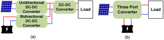
Figure 1.
Renewable power systems: (a) separate DC–DC converter, and (b) three-port converter (TPC).
The PV input port is connected to a unidirectional DC–DC converter to supply power to the load and the energy storage port is connected to a bidirectional DC–DC converter to maintain the power balance. These two DC–DC converters could be designed separately. However, compared to the three-port converter (TPC) shown in Figure 1b, this arrangement does not allow components to be multiplexed and more components need to be utilized to achieve a high voltage gain [6]. It has been found that due to its advantages of integrated multiplexing components, high power efficiency, unified power-control strategy, and low costs, the TPC is increasingly attracting the attention of designers [7].
TPCs can be classified as isolated, partly isolated, and nonisolated. Among these types, the isolated type is typically selected to achieve a high step-up voltage gain [2]. However, this type has several drawbacks including a larger volume and higher costs due to its multiwinding transformer [1]. As a result, the need for high voltage gain and a small size seems contradictory so it is worth addressing this tradeoff.
Due to the promising prospects of the TPC as a good substitute for a separate DC–DC converter, a large number of studies have focused on its variable topology and unified control strategy [6,8,9,10,11,12,13,14,15,16]. Boost-based, buck–boost-based, and SEPIC-based topologies have been developed [10] and researchers have achieved a TPC with fewer components [8,15]. In order to establish a general principle and method, a TPC with a programmable topology and its generalized analysis have been reported [13]. The authors discuss the general principle and the programmable approach of deriving multiple viable integrated topologies, from which several viable topologies are conveniently derived from multiple possible connections. Furthermore, five power transmission paths and topological structures of the TPC have been proposed and the derivation of TPC topologies has been systematically explored to establish a practical and universal principle [2]. In addition to the above, integrated and unified power control strategies have also been introduced, where switch methods in different operation modes have been discussed at length and three-port power quality could be reliably guaranteed [7,17,18,19,20]. Simultaneously implementing the strict output voltage requirements and maximum power point tracking (MPPT) of the PV system can make the most of existing renewable energy sources. These strategies are based on the control principle that for an N port converter system, N-1 control input variables are necessary [18]. To simplify this complicated MIMO system, a decoupling network has been proposed, which involves designing closed-loop compensators for each control loop. The above studies mainly focus on the integration of the topology and the topic of high step-up voltage gain is not considered in detail so the above-mentioned problems need to be addressed. A high-voltage nonisolated converter using a coupled inductor has been proposed [21,22,23,24] and a step-up TPC based on the Luo topology with one switch has also been proposed [25]. However, since each of the three ports has its own conversion circuit and lacks multiplexing components, these TPCs cannot be used in renewable energy applications without a unified power-control strategy. Therefore, this article proposes an integrated nonisolated TPC that is not only capable of high step-up voltage gain but also utilizes a unified power-control strategy. The ultimate goal is to make this TPC available for solar PV applications.
To further illustrate the features of the proposed converter, the topology of this TPC is compared to the above-mentioned topology, as shown in Table 1. A unified power-control strategy that meets the requirements of a stable load power supply and maximum utilization of the renewable energy system is also discussed. This research subject can be subdivided into roughly two aspects. On the one hand, some two-port DC–DC converters can be used to derive a nonisolated TPC, but they are incapable of a high step-up voltage gain. Therefore, the aim of this research is to improve one DC–DC converter and make it capable of a high voltage gain. On the other hand, a significant step toward achieving this goal is by adding an energy storage port to the above two-port converter with a reasonable derivation principle and method that allows it to be integrated.

Table 1.
Comparison with similar topologies.
This article offers the following contributions:
- An integrated TPC is proposed and analyzed that makes it possible for solar PV applications to achieve a high step-up gain without a separate DC–DC converter.
- Fewer components and a nonisolated-type TPC without multiwindings are necessary to decrease the costs and volume.
- One reliable and unified power-control strategy is proposed to respond to transience in the input and load.
The organization of this article is as follows. In Section 2, the operational principle of the proposed TPC is discussed and the steady-state characteristics are analyzed to achieve a static voltage gain. In addition, the TPC is modeled using both average-state and small-signal models to design a power-control strategy that meets the requirements of MPPT in PV and can handle possible instantaneous situations such as fluctuating loads or sudden environmental changes in solar PV. The experimental results are presented in Section 3 to confirm the above analysis. Finally, the conclusions of this article are presented in the last section.
2. Analysis of the Proposed Converter
As seen in Figure 2a, the primary inductor is connected to a conventional SEPIC converter, and reducing the current ripple and output port could lead to a positive voltage, which are the main reasons that a SEPIC converter is used extensively for renewable energy. Furthermore, as shown in Figure 2b, a modified SEPIC converter is derived from the conventional SEPIC converter by adding only one diode and one capacitor . This modified method allows the two-port SEPIC converter to achieve a higher voltage gain, which is the basis of the future development of TPCs. In order to systematically identify typical derivation methods for TPCs, researchers have recombined and optimized existing topologies from a power flow perspective. They achieved this by combining branch methods that offer the same performance [10]. Moreover, several methods for deriving integrated TPCs have been graphically illustrated and extensively studied [8]. The proposed TPC was obtained through the topological derivation method mentioned above, as shown in Figure 2c. In this topology, the additional diode connects with in series. Similarly, the additional switch connects with in series, which provides a branch for the energy storage port. As a result, the proposed TPC can be integrated with the above-mentioned additional components. Figure 2 demonstrates the generation process of the modified SEPIC TPC.
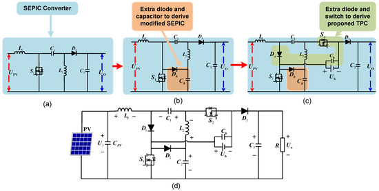
Figure 2.
Topology derivation: (a) conventional SEPIC converter, (b) modified SEPIC converter, (c) proposed converter topology, and (d) redrawing of proposed TPC.
The proposed converter is redrawn in Figure 2d and contains two inductors ( and ), three capacitors (, , and ), three diodes (, , and ), and only two switches ( and ). In order to analyze the performance of the proposed TPC, the operational principle, steady-state characteristics, small-signal model, and power-control strategy of the proposed converter are described theoretically in this section. During the steady-state analysis, the high voltage gain is introduced, and a state-space equation is derived for designing the control strategy, as analyzed in the small-signal model. Moreover, as the electrical equipment connected with each different port exhibits diverse output performance, the control strategy needs to accommodate the diverse control requirements of the three different ports.
2.1. Operational Principle
The definitions of the symbols used below are explained here. and are the currents flowing through inductors and . and are the currents flowing through capacitors and . is the current of the battery, where the discharging current is defined as greater than 0. and are the currents of diodes and . and are the currents flowing through switches and . and represent the driving signals of switches and . and , respectively, represent the voltage in the PV input port and the voltage in the energy storage port.
There are two possible cases for the drive signal, and . The typical waveforms of several components in the proposed TPC operating in continuous current mode (CCM) are illustrated in Figure 3e. Notably, these two different cases switch automatically based on the relationship between duty ratios and .
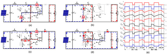
Figure 3.
Equivalent circuits of the proposed TPC in (a) State I, (b) State II, (c) State III, and (d) State IV. (e) Waveforms of key components.
Different states correspond to different working circuits. The current circuits in the equivalent circuits of all states are indicated in Figure 3. Based on Kirchhoff’s Voltage Law (KVL), the different branches of the two inductors are represented by different colors in Figure 3 and the operating modes are described below.
State I (see Figure 3a): Both and are ON. Diodes , , and are reverse-biased. The battery discharges to transfer energy to inductor . Inductors and absorb energy from the PV module and battery via and , respectively; thus, inductor currents and increase linearly. In this state, the energy from the PV module and battery can be seen to transfer to inductors and .
State II (see Figure 3b): is ON and is OFF. Diode is turned on to provide an energy loop for inductors and , whereas diodes and are still reverse-biased. The battery will not operate in this state. Inductors and absorb energy from the PV module and capacitor via and . In this state, the inductor currents and continue to increase linearly, even though the battery is not charging or discharging.
State III (see Figure 3c): is OFF and is ON. Diode is turned on to provide an energy loop for the load, whereas diode is still reverse-biased. Inductors and release energy via and . In this state, capacitor is charged by and the inductor currents and start to decrease linearly.
State IV (see Figure 3d): Both and are OFF. Diodes , , and turn on. The battery is charging while inductors and release energy via and , respectively. At the same time, capacitor is charged by . In this state, it can be seen that the energy from the PV module and battery temporarily stored in the inductors starts to be transferred to the load; thus, the output voltage obtains a step-up gain.
With the exception of the above-mentioned normal situation, when the PV module does not generate any power and only the battery provides power to the load, the proposed converter can still operate normally. In this situation, by controlling duty ratio of switch with remaining off, the energy is exchanged among the battery, , , , and load, and the output voltage can remain constant.
2.2. Steady-State Characteristics
To illustrate the steady-state characteristics of the proposed TPC, the working performance of the key components such as the capacitors and inductors in every state mentioned above needs to be studied in detail. The currents flowing through capacitors and and the voltages applying to inductors and are the focus of this section and the equations are given below.
In State I, inductors and absorb external energy, the voltages applied to and start to increase steadily, and both capacitors and release their own energy. Building on the previous analysis of the equivalent circuits, the expressions of the key components during State II, State III, and State IV can be formulated using the same method, as shown in Equation (1).
Based on the voltage-second balance principle, the voltages applied to inductors and are considered constant, and the relationship between them can be expressed as in Equation (2)
The static gain of the proposed TPC can be obtained by taking into account the voltage-second balance in and at the steady state in CCM, and the relationship between , , and can be summarized, as in Equation (3).
Based on the same voltage-second balance principle in inductors and , for the TPC based on a conventional boost converter or SEPIC converter [10], the output voltage gain can also be considered by using the voltage-second balance principle, as in Equation (4) and Equation (5), respectively. It is clear that with the same values of and , the proposed TPC can achieve a higher output voltage.
When the PV input voltage is 15 V and the energy storage voltage is 40 V, and can be calculated as 0.51 and 0.32, respectively, to achieve a 150 V output voltage for the proposed TPC. In Equation (3), it can be seen that the output voltage is affected by both and . To further illustrate the high-voltage-gain characteristic of the proposed TPC compared to a conventional TPC, it is demonstrated that the proposed TPC can achieve a higher voltage by maintaining while varying from 0 to 0.6, as seen in Figure 4a. Similarly, this distinct advantage of the proposed TPC can also be demonstrated by maintaining , as seen in Figure 4b.
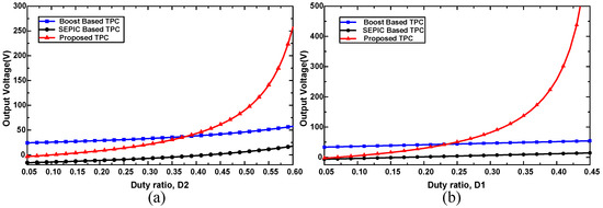
Figure 4.
Comparison of static gains in the above-mentioned TPC. (a) Output voltage when , and (b) output voltage when .
Figure 5 presents the waveform of , where is the average current of during one switch cycle . can also be denoted as , where is the average current of the ripple current. The slope of can be expressed as in Equation (6).
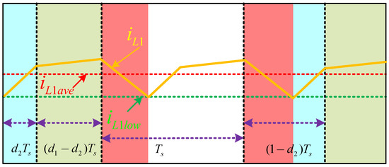
Figure 5.
The waveform of .
As shown in Figure 5, the ripple current can be expressed as in Equation (7)
and the average current of can be expressed as in Equation (8). Inductor absorbs or releases no energy during one switch cycle; thus, the relationship between and can be derived as in Equation (9).
By combining Equations (7) and (9), it can be seen that duty ratio or can significantly affect ; therefore, the ranges of and must be considered when selecting the value of inductor . Similarly, combining Equations (8) and (9) leads to the reasonable conclusion that or can control , which is equivalent to the PV module output current . This implies that the duty ratio plays an important role in the PV module control strategy, and thus, or can be set as a control variable to regulate solar PV.
2.3. Small-Signal Model and Power-Control Strategy
Before discussing the dynamic characteristics of the proposed TPC, it is important to note that in a short switching cycle, the variables can be assumed to have an average value. Therefore, the large-signal model can be expressed as in Equation (10).
The output variables, state variables, and input voltages x contain two components: steady-state value X and perturbation value . Considering the perturbations of the variable, by substituting into Equation (10) and neglecting the second-order terms [26,27], the state-space representation of the proposed TPC can be described in the small-signal model, which is shown in Equation (11).
where
The power-control strategy aims to achieve a stable output voltage with good dynamic characteristics. This power-control strategy focuses on PWM modulation and MPPT. As seen in Figure 6, in the perturbation and observation methods, and are sampled to achieve MPPT while is regulated. is regulated by PI control with a reference value of the output voltage .
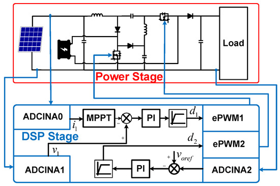
Figure 6.
Control block diagram of the proposed TPC.
Substituting the parameters given in Table 2 into Equation (11), the bode diagrams of two transfer functions and are obtained, as shown, respectively, in Figure 7a,b. By designing a compensation control strategy, the phase margins of these two closed loops are and , respectively, which satisfies the stability requirements of the proposed TPC system.
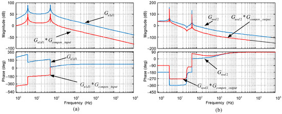
Figure 7.
Bode diagrams of two transfer functions. (a) Input loop, (b) output voltage loop.
On the one hand, the MPPT control in the input port can maximize the use of solar PV. There are many existing MPPT control methods, such as the conductivity increment method and disturbance observation method. However, the research focus of this paper is not on the MPPT strategy itself so only a simple constant-voltage control method is adopted. On the other hand, the constant-voltage control strategy applied to the output port can meet the requirements of a constant-voltage load, but this is only one example of output control. If the load switches to a constant power type, the control strategy should be adjusted accordingly.
It can be seen in the above illustrations that the control strategies in different ports can be designed in an independent control loop without loop coupling, which greatly simplifies the control design of the other TPCs.
3. Experimental Results and Analysis
The proposed 100 W TPC is established using the component parameters shown in Table 2. In the SimStar MT3200 HIL experimental platform shown in Figure 8, the energy storage port is supplied by a 40 V lead-acid battery, and an APM36M5W25X24-type solar PV with a maximum power of 100 W is used, whose parameters are also shown in Table 2. The operational principle and the steady- and dynamic-state waveforms are tested and verified on this platform. In the experiment, the waveforms of the key components in a switching cycle are measured and compared with the previous working state. Moreover, transient analysis of the proposed TPC is also performed by suddenly mutating the PV input port and load output port to simulate the changes in irradiance, temperature, and load that occur in real situations. Furthermore, the operative mode of the proposed TPC is tested and verified under the circumstance of only one battery providing power to the load.
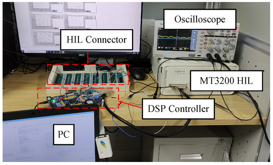
Figure 8.
SimStar MT3200 HIL experimental platform.
Table 2.
Circuit parameters.
Table 2.
Circuit parameters.
| Circuit Parameters | Values | PV Parameters | Values |
|---|---|---|---|
| Input Voltage | 10 V∼30 V | PV Type | APM36M5W25X24 |
| Battery Voltage | 30 V∼50 V | Open Circuit voltage | 20 V |
| Output Voltage | 150 V | Short Circuit Current | 0.32 A |
| Input Current | 0 A∼7.04 A | Maximum Operating Point Voltage | 15 V |
| Switching Frequency | 50 kHz | Maximum Operating Point Current | 0.3 A |
| Capacitor | 2000 F | Number of Cells in Parallel | 22 |
| Capacitor | 500 F | Number of Cells in Series | 1 |
| Capacitor | 5000 F | Maximum Power of Photovoltaic Array | 100 W |
| Inductor | 2000 H | Temperature | C |
| Load | 225 | Irradiance | 1000 W/m |
3.1. Steady-State Performance
The waveforms of and and inductor currents and in two different cases, where and , are presented in Figure 9. These two cases illustrate the possible process of power conversion. These waveforms are consistent with the theoretical analysis shown in Figure 3e, which proves that the operational mode of the proposed TPC meets the expectations.
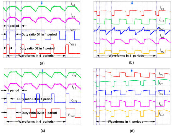
Figure 9.
Steady-state waveforms of (a) , , , when , (b) , , , , and when , (c) , , , when , (d) , , , , and when .
In a steady state, the currents of and decrease after two increasing periods, as shown in Figure 9a,c, where the average current of is equal to the current of the PV input to the system. The current flowing through capacitors and and switches and is shown in Figure 9b,d. According to the experimental verification results, the steady-state operation of the components meets the expectations of the theoretical analysis. For the steady-state experiment, Figure 9 shows the waveform details for a total of five periods; within a period, the inductance currents and both increase linearly in the first two stages and decrease linearly in the third stage, depending on the relationship between the two duty ratios and , as shown in Figure 5.
3.2. Dynamic-State Performance
On the one hand, as shown in Figure 10, to simulate a sudden change in solar PV, the PV irradiance is set by decreasing the value from 1000 W/m to 800 W/m and maintaining it at . Although the input power from PV decreases, as the waveforms of and show, with the MPPT control strategy, PV reaches a new maximum power point of 75 W with and . The output port would release less energy based on the former three-port power situation. To meet the power demands of the load, the energy storage port starts releasing more energy to compensate for the reduced part, as shown in Figure 10b. The average current output from the energy storage port increases by 0.9 A, while at the same time, output voltage quickly returns to and maintains a value of 150 V within 0.6 s and the output port maintains and exports 100 W to the load. The PV power decrease in the experiments illustrates the energy storage port’s role in balancing power by absorbing or compensating for energy in the TPC. Throughout the entire experiment, the PV fully converts energy into the TPC under MPPT control. In addition, inductor currents and fluctuate within a range of 2 A, mainly because the inductors are charged and discharged in every period. The fluctuations in the waveforms are also shown in Figure 10b.
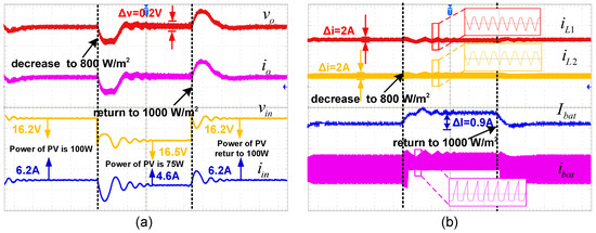
Figure 10.
Dynamic waveforms of (a) , , , and , and (b) , , , and during input transience.
On the other hand, as shown in Figure 11, to simulate a sudden change in load, the load is decreased from 100% to 75% while the irradiance and temperature of the solar PV remain at 1000 W/m and C, respectively. In this case, the solar PV power remains at 100 W with MPPT control, and input voltage and input current remain unchanged at A and V. However, the output port needs to export less energy to meet the decreased power demand, as shown in Figure 10b, and the average current output from the energy storage port increases by 0.8 A. Thus, the energy storage port absorbs the former surplus energy and establishes a new power balance for the three ports within 0.4 s. In the meantime, output current decreases from 0.66 A to 0.5 A. Throughout the experiment, the output voltage is maintained at 150 V under constant voltage control in the output port.
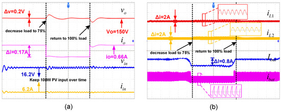
Figure 11.
Dynamic waveforms of (a) , , , and , and (b) , , , and during load transience.
The designed control strategy enables all three ports to achieve a new power balance and satisfy the requirements of their respective port operating characteristics, regardless of whether the change occurs in the PV input port or output load port. This is mainly due to the charging and discharging functions of the energy storage port.
3.3. Performance When Only Battery Provides Power
For a possible situation in which PV provides no power to the load, it is necessary to discuss the reliability of the operation of the proposed TPC. To simulate this situation, the output power of the solar PV is set to zero, as seen in the waveforms of and in Figure 12a. The load only obtains energy from energy storage while switch remains off, i.e., . In this case, the PV MPPT control strategy of the input port does not need to be applied, and another control variable (duty cycle of switch ) remains under the constant-voltage control of the output port. Within 0.5 s, the input power of the PV is cut off and the energy of the load is only provided by the energy storage port. In this case, the average current of the energy storage port releases another 3 A to supply power to the load. During the entire period, switch is not involved in control. Therefore, the original three stages in one period are reduced to two stages, and the currents of the two inductors only increase linearly in one stage and decrease in the last stage, as shown in Figure 12b.
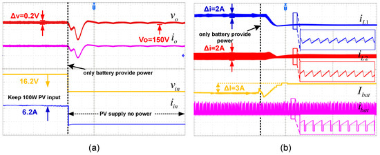
Figure 12.
Waveforms of (a) , , , and , and (b) , , , and when only the battery provides power.
3.4. Efficiency
Under different voltage and power levels, the loss of energy on the transmission path or in components such as diodes and switches is different. There are also some differences in power efficiency among the three ports. In order to analyze and identify the power efficiency range of the proposed TPC, we varied the output power level from 100 W to 200 W and the output power voltage level from 80 V to 150 V. The power efficiency of the proposed TPC related to different output voltages and output powers is shown in Figure 13. As the input and output currents of the energy storage port are determined by external circuits within each period, when the input power and load power are similar, from the perspective of power balance, it is ideal for the average current of the energy storage port to be 0 within a cycle. However, this condition cannot be satisfied under the influences of the duty ratio and external component parameters so at this time, the power loss is the largest. When the load power is significantly greater than or less than the input power, the energy storage section can release or absorb energy and the power loss will be smaller. The input power of the proposed TPC is set to 100 W; therefore, when the output power is around 100 W, regardless of the output voltage, the power efficiency among the three ports reaches 85%, the minimum efficiency of the proposed TPC. With the increase in the output power level, the efficiency starts to increase. From the perspective of the output voltage level, a higher voltage output level is often associated with lower power efficiency because increasing output currents consume power from the energy storage port to a greater extent. However, all of the power efficiencies are higher than 85% and most of them have reached the range of 90% to 94%.
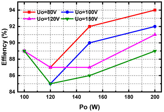
Figure 13.
Efficiency curve of proposed TPC.
4. Conclusions
This study introduces an integrated nonisolated three-port converter (TPC) with a high step-up voltage gain that interfaces solar PV, energy storage, and load. Comparative research with other TPCs, such as a boost-based TPC and SEPIC-based TPC, explains in detail the advantages of this proposed TPC, which includes a high step-up voltage gain and eliminates the need for a large volume transformer. Additionally, the proposed TPC reduces the number of components as much as possible. From the perspective of the circuit topology, it is an attractive point that only two switches and two diodes are required to obtain a nonisolated TPC, which is adopted to address the contradiction between the voltage gain and nonisolated-type converter. Moreover, an effective power control strategy is proposed based on the large-signal model and small-signal model, ensuring steady- and dynamic-state performances with considerable efficiency. Meanwhile, the proposed loop design features less coupling, which greatly reduces the complexity of the control strategy. Experimental results from SimStar MT3200 HIL verify the feasibility of the proposed TPC and its power control strategy. The dynamic-state performance illustrates that a new power balance can be achieved within at most, which is a clear advantage of the integrated TPC. In contrast, a separate three-port DC–DC converter may require a communication delay to establish a new power balance. In general, the modified SEPIC TPC demonstrates the expected performance in terms of the step-up voltage gain, compact topology, component layout, and the reliability of the control strategy. Furthermore, the design and derivation process of the proposed TPC can serve as a reference for the development of additional TPCs.
Author Contributions
Conceptualization, Y.Z. and Y.H.; methodology, Y.Z. and S.L.; software, S.L. and J.W.; validation, Y.W., Y.H. and Z.C.; formal analysis, S.L.; investigation, J.W.; resources, Z.C.; data curation, Y.H.; writing—original draft preparation, S.L.; writing—review and editing, Y.Z.; visualization, Y.W.; supervision, Y.H.; project administration, Y.Z.; funding acquisition, Z.C. All authors have read and agreed to the published version of the manuscript.
Funding
This work was supported by the National Natural Science Foundation of China under Grant 52277007.
Data Availability Statement
The data presented in this study are available on request from the corresponding author.
Conflicts of Interest
The authors declare no conflict of interest.
References
- Bhattacharjee, A.K.; Kutkut, N.; Batarseh, I. Review of Multiport Converters for Solar and Energy Storage Integration. IEEE Trans. Power Electron. 2019, 34, 1431–1445. [Google Scholar] [CrossRef]
- Wang, Z.; Luo, Q.; Wei, Y.; Mou, D.; Lu, X.; Sun, P. Topology Analysis and Review of Three-Port DC–DC Converters. IEEE Trans. Power Electron. 2020, 35, 11783–11800. [Google Scholar] [CrossRef]
- Chaudhury, T.; Kastha, D. A High Gain Multiport DC-DC Converter for Integrating Energy Storage Devices to DC Microgrid. IEEE Trans. Power Electron. 2020, 35, 10501–10514. [Google Scholar] [CrossRef]
- Faraji, R.; Farzanehfard, H. Fully soft-switched multiport DC–DC converter with high integration. IEEE Trans. Power Electron. 2020, 36, 1901–1908. [Google Scholar] [CrossRef]
- Jiang, W.; Fahimi, B. Multiport Power Electronic Interface—Concept, Modeling, and Design. IEEE Trans. Power Electron. 2011, 26, 1890–1900. [Google Scholar] [CrossRef]
- Chien, L.J.; Chen, C.C.; Chen, J.F.; Hsieh, Y.P. Novel Three-Port Converter With High-Voltage Gain. IEEE Trans. Power Electron. 2014, 29, 4693–4703. [Google Scholar] [CrossRef]
- Gao, M.; Wang, S.; Yu, W.; Liu, T.; Shi, J. Analysis of a coupled inductor boost three-port converter with high voltage gain for renewable energy systems. J. Power Electron. 2022, 22, 2100–2121. [Google Scholar] [CrossRef]
- Cheng, T.; Lu, D.D.C.; Qin, L. Non-Isolated Single-Inductor DC/DC Converter With Fully Reconfigurable Structure for Renewable Energy Applications. IEEE Trans. Circuits Syst. II Express Briefs 2018, 65, 351–355. [Google Scholar] [CrossRef]
- Zhou, G.; Tian, Q.; Wang, L. Soft-Switching High Gain Three-Port Converter Based on Coupled Inductor for Renewable Energy System Applications. IEEE Trans. Ind. Electron. 2022, 69, 1521–1536. [Google Scholar] [CrossRef]
- Wu, H.; Sun, K.; Ding, S.; Xing, Y. Topology Derivation of Nonisolated Three-Port DC–DC Converters From DIC and DOC. IEEE Trans. Power Electron. 2013, 28, 3297–3307. [Google Scholar] [CrossRef]
- Moradisizkoohi, H.; Elsayad, N.; Mohammed, O.A. A Family of Three-Port Three-Level Converter Based on Asymmetrical Bidirectional Half-Bridge Topology for Fuel Cell Electric Vehicle Applications. IEEE Trans. Power Electron. 2019, 34, 11706–11724. [Google Scholar] [CrossRef]
- Zhu, H.; Zhang, D.; Zhang, B.; Zhou, Z. A Nonisolated Three-Port DC–DC Converter and Three-Domain Control Method for PV-Battery Power Systems. IEEE Trans. Ind. Electron. 2015, 62, 4937–4947. [Google Scholar] [CrossRef]
- Chen, G.; Jin, Z.; Liu, Y.; Hu, Y.; Zhang, J.; Qing, X. Programmable Topology Derivation and Analysis of Integrated Three-Port DC–DC Converters With Reduced Switches for Low-Cost Applications. IEEE Trans. Ind. Electron. 2019, 66, 6649–6660. [Google Scholar] [CrossRef]
- Liu, W.S.; Chen, J.F.; Liang, T.J.; Lin, R.L. Multicascoded sources for a high-efficiency fuel-cell hybrid power system in high-voltage application. IEEE Trans. Power Electron. 2010, 26, 931–942. [Google Scholar] [CrossRef]
- Al-Soeidat, M.R.; Aljarajreh, H.; Khawaldeh, H.A.; Lu, D.D.C.; Zhu, J. A Reconfigurable Three-Port DC–DC Converter for Integrated PV-Battery System. IEEE J. Emerg. Sel. Top. Power Electron. 2020, 8, 3423–3433. [Google Scholar] [CrossRef]
- Dobakhshari, S.S.; Fathi, S.H.; Milimonfared, J. A New Soft-Switched Three-Port DC/DC Converter With High Voltage Gain and Reduced Number of Semiconductors for Hybrid Energy Applications. IEEE Trans. Power Electron. 2020, 35, 3590–3600. [Google Scholar] [CrossRef]
- Wang, L.; Wang, H.; Fu, M.; Liang, J.; Liu, Y. A Three-Port Energy Router for Grid-Tied PV Generation Systems With Optimized Control Methods. IEEE Trans. Power Electron. 2023, 38, 1218–1231. [Google Scholar] [CrossRef]
- Qian, Z.; Abdel-Rahman, O.; Al-Atrash, H.; Batarseh, I. Modeling and Control of Three-Port DC/DC Converter Interface for Satellite Applications. IEEE Trans. Power Electron. 2010, 25, 637–649. [Google Scholar] [CrossRef]
- Subramanian, A.; Karuppiah, S. Analysis of dual-input three-port isolated DC–DC converter with bidirectional capability. J. Power Electron. 2022, 22, 711–726. [Google Scholar] [CrossRef]
- Zhang, J.; Wu, H.; Qin, X.; Xing, Y. PWM Plus Secondary-Side Phase-Shift Controlled Soft-Switching Full-Bridge Three-Port Converter for Renewable Power Systems. IEEE Trans. Ind. Electron. 2015, 62, 7061–7072. [Google Scholar] [CrossRef]
- Gules, R.; dos Santos, W.M.; dos Reis, F.A.; Romaneli, E.F.R.; Badin, A.A. A Modified SEPIC Converter With High Static Gain for Renewable Applications. IEEE Trans. Power Electron. 2014, 29, 5860–5871. [Google Scholar] [CrossRef]
- Zhu, Y.; Wang, Y.; Teng, J.; Sun, X.; Qi, M.; Zhao, W.; Li, X. Partial Power Conversion and High Voltage Ride-Through Scheme for a PV-Battery Based Multiport Multi-Bus Power Router. IEEE Access 2021, 9, 17020–17029. [Google Scholar] [CrossRef]
- Hasanpour, S.; Baghramian, A.; Mojallali, H. A Modified SEPIC-Based High Step-Up DC–DC Converter With Quasi-Resonant Operation for Renewable Energy Applications. IEEE Trans. Ind. Electron. 2019, 66, 3539–3549. [Google Scholar] [CrossRef]
- Wang, J.; Wu, X.; Liu, Z.; Cui, X.; Song, Z. Modified SEPIC DC-DC Converter with Wide Step-up/Step-down Range for Fuel Cell Vehicles. IEEE Trans. Ind. Electron. 2022, 1–15. [Google Scholar] [CrossRef]
- Ghasemi, F.; Yazdani, M.R.; Delshad, M. Step-Up DC-DC Switching Converter With Single Switch and Multi-Outputs Based on Luo Topology. IEEE Access 2022, 10, 16871–16882. [Google Scholar] [CrossRef]
- Nejabatkhah, F.; Danyali, S.; Hosseini, S.H.; Sabahi, M.; Niapour, S.M. Modeling and Control of a New Three-Input DC–DC Boost Converter for Hybrid PV/FC/Battery Power System. IEEE Trans. Power Electron. 2012, 27, 2309–2324. [Google Scholar] [CrossRef]
- Elserougi, A.; Abdelsalam, I.; Massoud, A.; Ahmed, S. A non-isolated hybrid-modular DC-DC converter for DC grids: Small-signal modeling and control. IEEE Access 2019, 7, 132459–132471. [Google Scholar] [CrossRef]


Disclaimer/Publisher’s Note: The statements, opinions and data contained in all publications are solely those of the individual author(s) and contributor(s) and not of MDPI and/or the editor(s). MDPI and/or the editor(s) disclaim responsibility for any injury to people or property resulting from any ideas, methods, instructions or products referred to in the content. |
© 2023 by the authors. Licensee MDPI, Basel, Switzerland. This article is an open access article distributed under the terms and conditions of the Creative Commons Attribution (CC BY) license (https://creativecommons.org/licenses/by/4.0/).