Abstract
This paper presents a variable-gain low-noise amplifier (VGLNA) based on an adaptive bias (ADB) circuit for the radar receiver front end. The ADB circuit processes the signal separated by a coupler at the LNA output port. First, the ADB circuit rectifies the coupled signal into positive DC voltage through a rectifier, which is then inverted to control a junction-gate field-effect transistor (JFET). The voltage-controlled current of JFET flows through a voltage-divider network and finally produces the DC biasing voltage for the BJT base termination, which decreases with the increase in the input RF power. The proposed VGLNA operates automatically in high gain at low input power and low gain at high input power, providing a wider dynamic range as compared to the constant-bias counterpart. For validation, a prototype is fabricated and measured at 6 GHz. As observed, the base biasing voltage generated by the ADB circuit is changed from 858 mV to 798 mV as the input power increases from −50 dBm to 0 dBm. As a result, the dynamic range represented by the input P1dB point (IP1dB) has an increase of 6.5 dB, while LNA still maintains a high gain of 15.15 dB at low input power.
1. Introduction
The radar systems are an electromagnetic system for the detection and location of the objects, and a low-noise amplifier (LNA) is considered a key component in its receiver front end [1,2,3]. Radar applications require a LNA, which can well process both weak and strong echos of the received signal. Specifically, in the case of an incoming weak signal, the LNA should provide high gain and minimum additive noise to increase the signal-to-noise ratio (SNR) of the signal. In contrast, for short-distance objects with high-power input signal, it is expected to operate at a low gain, which can exhibit good linearity or a wide dynamic range to avoid the saturation of the receiver chain. Therefore, a mechanism of gain control is necessary in the LNA design to achieve both these two objectives simultaneously, which cannot be solved with the common fixed-gain LNAs. In addition, in the case of sensing platforms, variable-gain LNAs (VGLNAs) research is essential because gain problems may occur depending on distance [4,5,6].
The VGLNAs have been developed for achieving a wide dynamic range as well as covering the entire detection range without the receiver signal saturation [7,8,9,10,11,12,13]. In [7,8], the authors proposed a method known as current steering, which controls gain through reducing the bias current and transconductance of the cascoded transistors. Another method is using an extra digital signal [9,10,11]. However, the use of the external control signal can increase receiver complexity and cause additional power consumption from digital circuits. Authors in [12] presented an automatic mechanism of gain control using an analog signal inside the circuit without external excitation. Nevertheless, the requirement of a multi-transistor adaptive biasing circuit leads to high design complexity, a large occupying area, and low accuracy in the discrete-circuit implementation. In [13], gain is automatically adjusted by a Gilbert-cell-based topology. However, this structure is also complicated and not suitable for discrete-circuit deployment.
In this paper, a single-ended VGLNA on the discrete-circuit implementation of a bipolar junction transistor (BJT) is designed with an extended dynamic range for a military radar receiver front-end at 6 GHz, which is in the C-Band, with the advantages of long-distance detection and low atmospheric attenuation, as compared to a higher frequency band. The VGLNA deploys a novel adaptive-biasing (ADB) circuit, which adopts a small part of the output analog signal to control gain in an automatic manner without another additional signal. The proposed ADB network is mainly a combination of a AC-DC converter and a resistive divider, which is one of the resistors realized by the equivalent ohmic operation of a junction field effect transistor (JFET). The main principle is to use the DC load signal from the rectifier to manipulate the equivalent resistor of the JFET source as JFET operates in the ohmic region. Following the design method, the dynamic range of LNA is extended significantly in comparison with that of the fixed-gain counterpart. It is also important to note that our research focuses on investigating and implementing the printed circuit board (PCB)-level LNA that relies on discrete components. PCB-level LNAs with ADB circuits have not been extensively studied, but the discrete circuits can offer advantages in terms of high performance, low complexity, and manufacturing cost compared to the integrated circuits.
2. Extended Dynamic Range with Lower Biasing Base Voltage
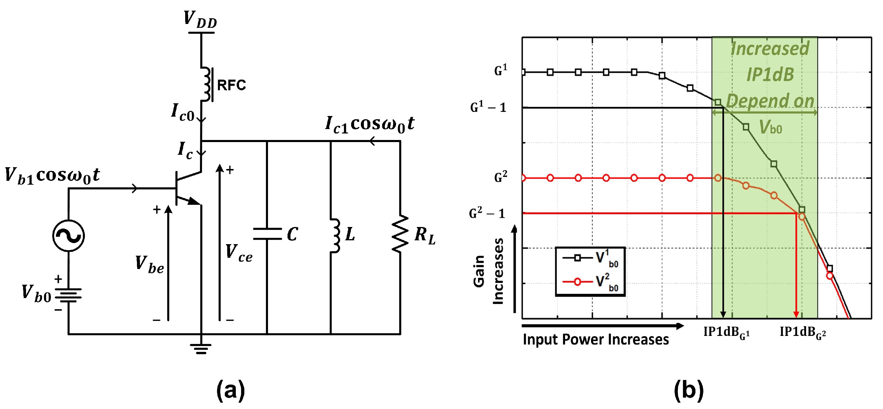
The generic schematic of a BJT-based LNA is shown in Figure 1a, where the active device is voltage-biased with two DC sources, i.e., and for base and collector terminations, respectively. For single-frequency operation, the dynamic range is commonly characterized by the input 1 dB compression point (IP1dB), which determines the input power at which LNA gain is dropped by 1 dB. In radar detection applications, it is always desirable to extend the IP1dB of LNA for processing near-distance objects with strong reflections in the linear region. The increase in the dynamic range, referred to as the increase in IP1dB, relates intimately to the decrease in the base biasing voltage , which can be demonstrated by considering the variation of BJT transconductance within small-to-large signal regimes. Assuming is the thermal voltage, transconductance is highest with small-signal driving, approximating and reducing as the input signal grows large. The large-signal transconductance associated with the input signal magnitude is then given by [14]
where denotes the saturated current, x is the base signal voltage amplitude, and is independent of and is defined as in [14]. It is clear that decreases with the increase in x or the signal magnitude . Additionally, the amplitude of depends on as described in (1). The slope of with respect to x is negative and can be calculated as follows:
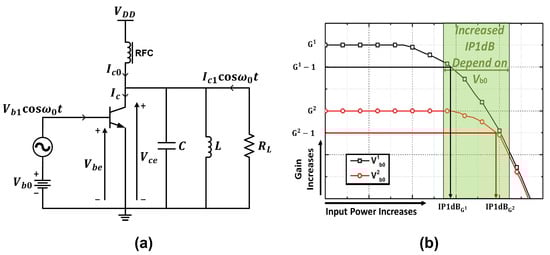
Figure 1.
(a) Generic LNA schematic with a bipolar transistor, and (b) input P1dB at different biasing point .
From (4), with the independence of on , and assuming that the is greater than , then becomes larger than . In other words, in the case of the biasing voltage is dropped quicker than with . As a result, IP1dB is higher with lower biasing voltage as intuitively illustrated in Figure 1b. The gain curve with respect to is more steep and descends to its IP1dB at a lower input power point, i.e., . However, LNA is also required to provide high gain to amplify the weak signals for long-distance detection to increase SNR, which is only obtained with high , for example, instead of in Figure 1b. Therefore, in order to achieve two targets concurrently, i.e., a wide dynamic range for processing the entire detection range without receiver saturation and a high initial gain for the weak signal amplification, a mechanism for changing the LNA gain according to the input power level has become a reliable approach and has been widely used in the radar detection applications. In this paper, the principle of reducing the base biasing voltage with the increase in input power is used to design the VGLNA.
3. VGLNA Design with ADB Circuit
The proposed VGLNA structure is shown in Figure 2, which commonly consists of input and output matching networks (MNs) to provide noise and power matchings for low noise figure (NF) and high gain. Specifically, the input MN is designed to match an intermediate impedance between noise and power impedances, which can provide a balanced performance of NF and gain, simultaneously, even in the whole variation range of .
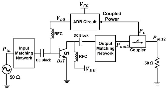
Figure 2.
Block diagram of the proposed VGLNA.
Instead of biasing the base terminal of BJT with a fixed DC source, LNA deploys an ADB circuit, which takes a small power proportion of the output signal through a coupler to generate a DC voltage for base biasing. As expected, the output DC voltage from the ADB circuit relates inversely to the input power, i.e., as the input power grows, reduces, and such variation leads to an extension of IP1dB.
The detail schematic of the proposed ADB circuit is shown in Figure 3. This network deploys an AC-DC converter, which rectifies the coupled signal into DC positive voltage . The rectifier topology utilizes a Schottky diode in a shunt, which was investigated in [15,16]. The RF coupled power is initially delivered through a rectifier input matching network to obtain a maximum signal across the diode. Then, the diode rectifies the negative half cycle of the signal, and the overall energy is stored in . The combined network of a RF choke and acts as a DC-pass filter, which smooths the rectified voltage. The DC output voltage determines the positive terminal of the inverse source and creates negative voltage on the other side to control the JFET current flowing in a voltage divider network. Finally, the voltage divider yields , exhibiting an inverse variation with the coupled signal power as shown in Figure 3.
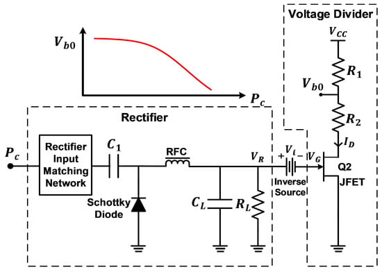
Figure 3.
Schematic of the proposed ADB circuit.
In order to clarify the relation between the resulting voltage and the input power , it is assumed that the coupler has the coupling coefficient of (dB) and LNA exhibits an initial gain of G(dB). The coupled power (dB) is calculated as follows:
From (5), and are in the same variation, and an increase in leads to an increase in as a result of the AC-DC converting process of the rectifier [15]. The DC inverse source then generates with the following relation:
For a depletion-mode JFET, the value of must be higher than to yield a negative value of for controlling the JFET current, which is calculated at different operating regions as follows [17]:
for saturation region and
for the ohmic region, where is the maximum saturation current, and is the pinched-off voltage. If JFET operates in the saturation region, is independent of as in (7), and apart from satisfying (7), must abide by Kirchhoff’s voltage law in the voltage divider network as follows:
Because is an increasing function of , then an increment of leads to higher , and will be reduced through the decrease in to satisfy (9). As another case of ohmic region, is dependent of , and JFET acts as a variable resistor , whose resistance value is defined as
where denotes the drain resistance at zero gate bias, i.e., . The voltage divider is then composed of three resistors (, , and ). As a result, can be calculated as follows:
It can be seen from (10) and (11) that has the same variation with and reduces with the increase in . In general, any operating region of JFET, the voltage divider can produce exhibiting an opposite variation with as well as the input power level. Because the required base biasing voltage is quite small for a BJT, just around practically, JFET is predicted to operate in the ohmic region. Additionally, the values of , and should be set such that at the starting time with , the maximum must be in the appropriate base–voltage range of the chosen BJT.
4. Implementation, Simulation and Experiment
For verification, the LNA is implemented on the Taconic TLY substrate (, mm) with a realistic BJT model operating at 6 GHz. Figure 4 shows the entire schematic of the proposed VGLNA. The input and output MNs deploy L-type sections of transmission lines (TLINs) to provide accurate noise and power matches for low noise figure (NF) and high gain, respectively. The RF chokes used in Figure 2 and Figure 3 are substituted by TLINs for minimizing losses at 6 GHz. The model and value of the components are listed in Table 1 for simulation and measurement.
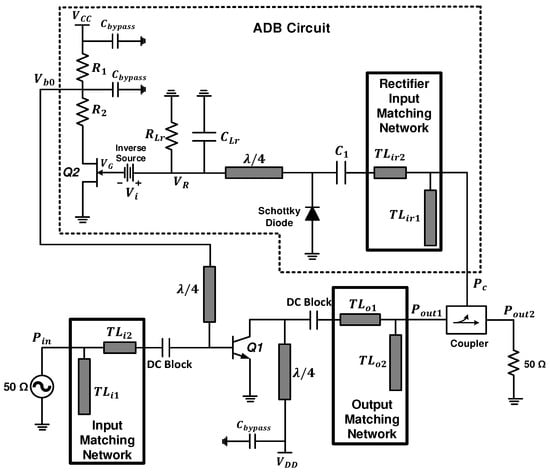
Figure 4.
The overall schematic of the proposed VGLNA.

Table 1.
Component models and values (implementation on 0.8-mm Taconic TLY-5) for simulation.
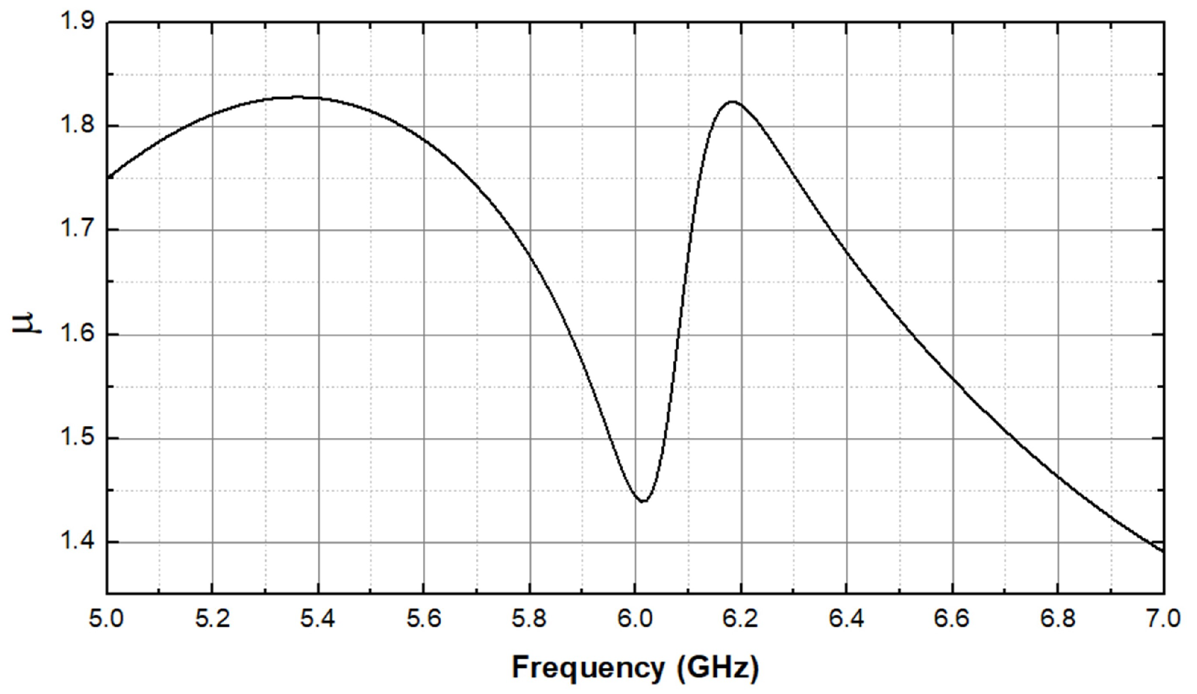
The stability factor of the proposed VGLNA is shown in Figure 5, which is higher than 1 within a tested wide bandwidth (5–7 GHz), indicating stable operation at the target frequency.
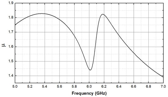
Figure 5.
Stability factor ( factor) of the proposed VGLNA.
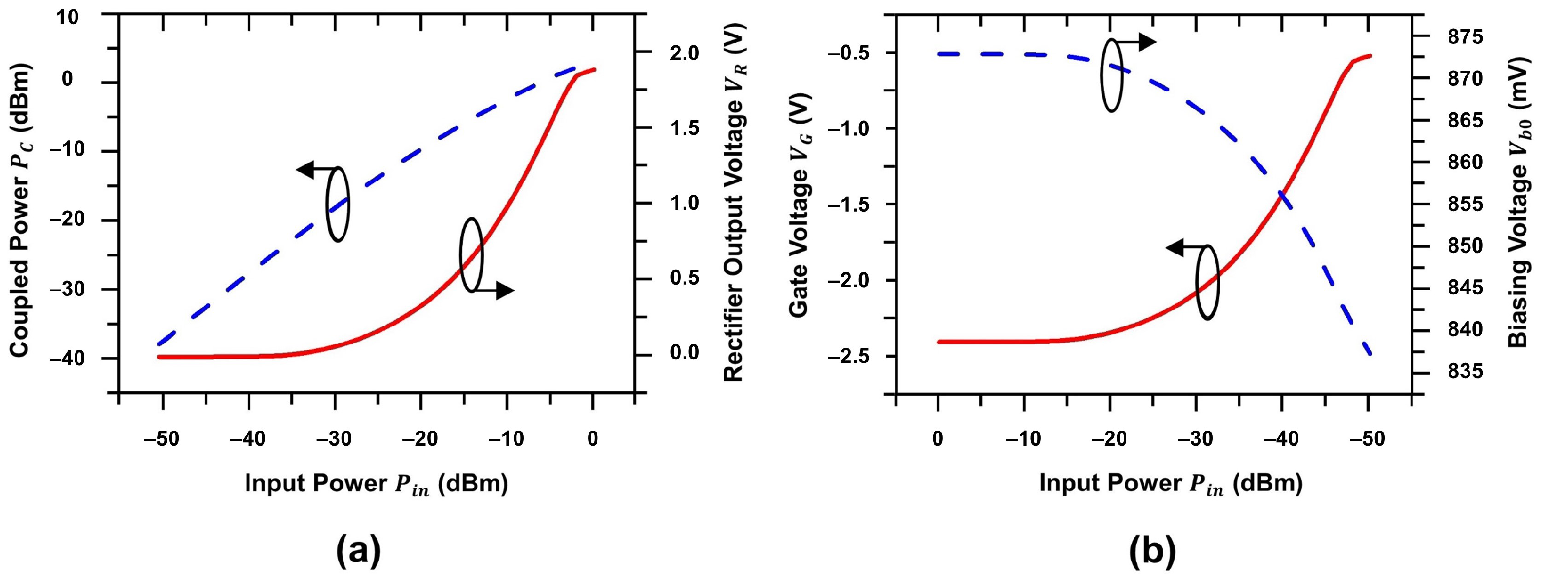
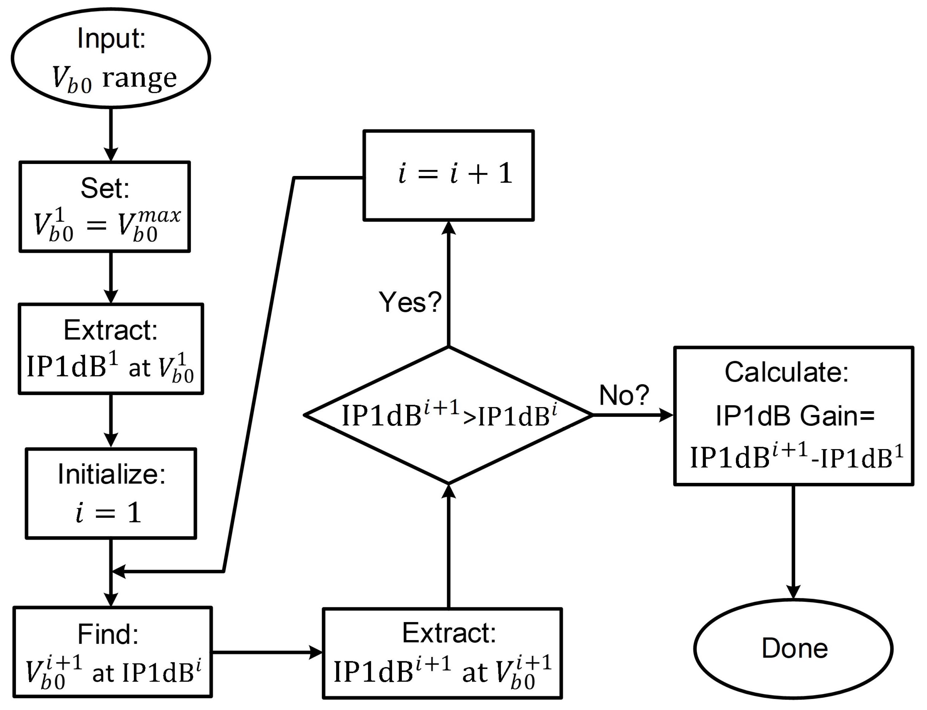
Figure 6 presents the variation of , , , and according to the input power spreading from dBm to 0 dBm. It can be seen that the coupled power exhibits a positive slope with and a high-enough value at dBm so that the rectifier can detect and rectify the wave. As a result, increases to the highest value of V at dBm; with V, changes from V to V during the input power range. This voltage controls the JFET current and generates the biasing voltage within a range from 873 mV to 837 mV as increases. To determine the IP1dB gain of the proposed VGLNA, fixed-bias LNA version of the same BJT is simulated at several different values of in the extracted range. The biasing voltage is first assigned to the highest value of the range, and its IP1dB is extracted. Then, this IP1dB is mapped to the range to determine the corresponding . Subsequently, the LNA is operated at that new with a new IP1dB. The process is repeated until the IP1dB gain is obtained as summarized in Figure 7. As shown in Figure 8a, with the adaptive-gain mechanism, the IP1dB gain is extended by dB, while also achieving a high gain of around dB at a low input power, which exhibits a clear advantage as compared to the fixed-bias counterpart at only V.
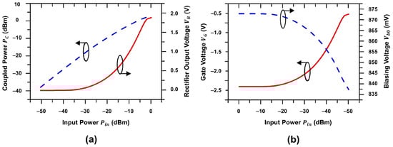
Figure 6.
(a) Simulated coupled voltage and rectifier output voltage , and (b) simulated gate voltage and biasing voltage .
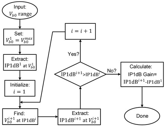
Figure 7.
Procedure of IP1dB gain extraction from a range.
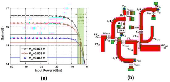
Figure 8.
(a) Simulated IP1dB gain of the proposed VGLNA at 6 GHz, and (b) layout for VGLNA fabrication.
For experimental validation, a prototype is fabricated and tested. The circuit layout is shown in Figure 8b. We use a total of three DC power supplies, i.e., , , and . A network analyzer is used first for measuring the S-parameters of the VGLNA. In this test, the initial gain of the VGLNA and its frequency response are observed. Then, the prototype is measured with a spectrum analyzer and a continuous-wave generator at the target frequency of 6 GHz to verify the adaptive gain behavior of the LNA. The trace of is performed thanks to a digital multimeter, which is used to calculate the IP1dB gain. Finally, the VGLNA experiences a noise analysis to determine its NF, which is important for practical radar applications.
4.1. S-Parameters
The S-parameters measurement setup is shown in Figure 9a, where three DC power supplies are V, and V as in the simulation. The analysis of S-parameters is performed by a network analyzer N5230C, and the results at dBm excitation are shown in Figure 9b. As observed, the reflection coefficients , are about dBm and dBm, respectively, at 6 GHz, confirming good impedance matching at the input and output terminals for power transmission. The transmission coefficient of the proposed VGLNA is achieved at 15.5 dB, denoting a high gain during the small-signal regime at the design frequency. The proposed LNA also exhibits an initial high gain across a very wide bandwidth, i.e., over 10 dB within a bandwidth from 0.5 GHz to 7.2 GHz, which is expected to operate well at different frequency bands. In addition, the VGLNA is compact, with its dimension shown in Figure 9c.
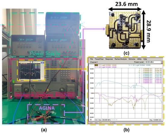
Figure 9.
(a) S-parameter measurement setup, (b) measurement results, and (c) circuit photograph.
4.2. IP1dB Gain and Linearity
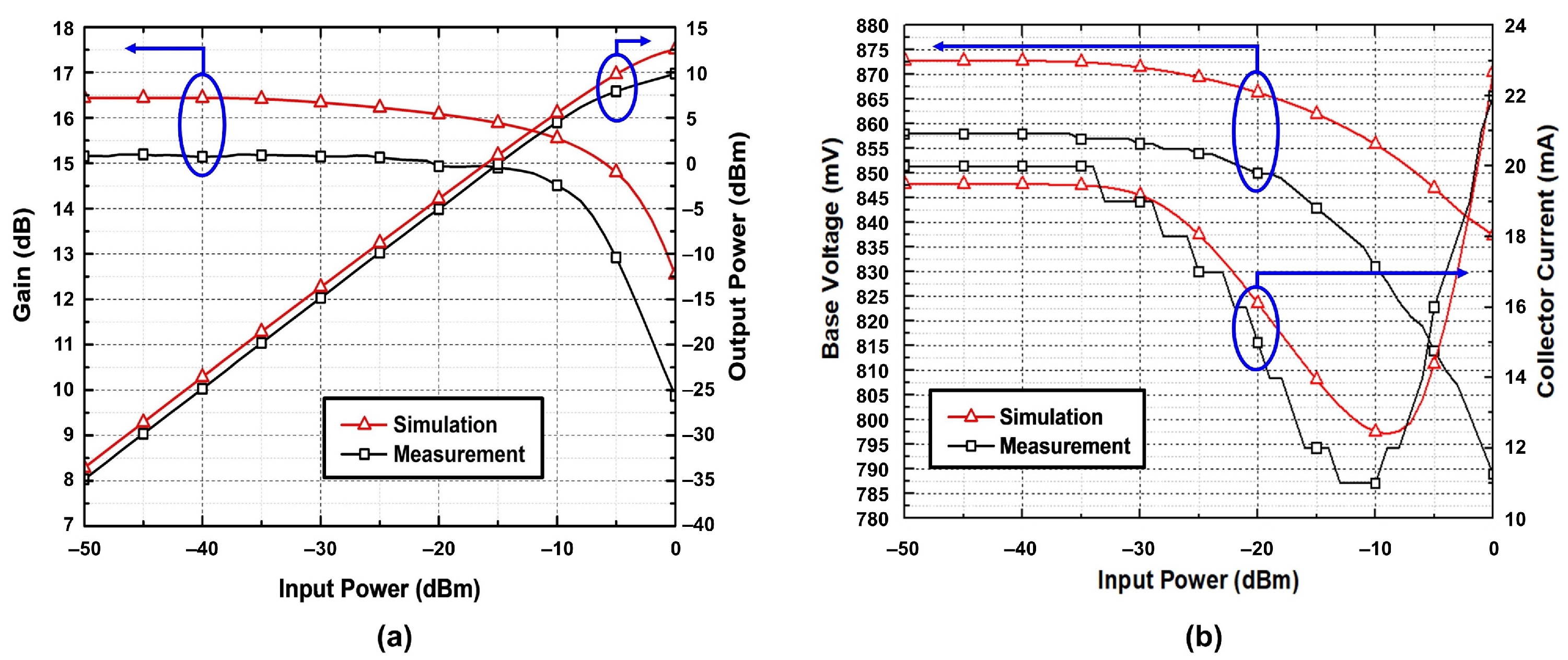
In order to evaluate IP1dB gain of our VGLNA at the target frequency, the prototype is measured under a signal generator and a spectrum analyzer. Similar to the S-parameters measurement setup, the circuit is applied with the same DC supplying voltages. A digital multimeter is used to measure the biasing voltage across the different input power levels. By sweeping the input power from −50 dBm to 0 dBm, a graph of gain and output power versus the input power is shown in Figure 10a. Note that these gain and output powers have different values from . The results show a similar tendency to the simulation ones, and it can be seen that the VGLNA always exhibits a gain of >10 dB within the overall input range. There is a slight difference in the initial gain between the two measurement schemes, i.e., using the S-parameters network analyzer and using the spectrum analyzer; due to their accuracy, there is instability in the cable loss and device characteristics. The overall range of is shown in Figure 10b. Increasing the input power from −50 dBm to 0 dBm, the observed voltage delivered to the base for biasing decreases from 858 mV to 798 mV. As a result, the DC collector current decreases, denoting a gain reduction mechanism in the LNA operation. It should also be noted that the similarity of the 1.2 dB lower measured gain (in comparison with the simulated gain while simulated) and the measured collector currents is due to the insertion loss of the coupler, which is not modeled accurately in the simulation.
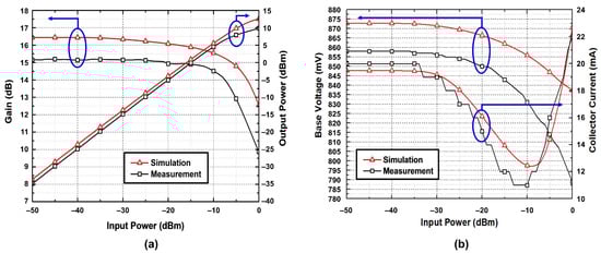
Figure 10.
(a) Measured gain and output power versus input power, (b) Base voltage and collector current measurement results based on input power.
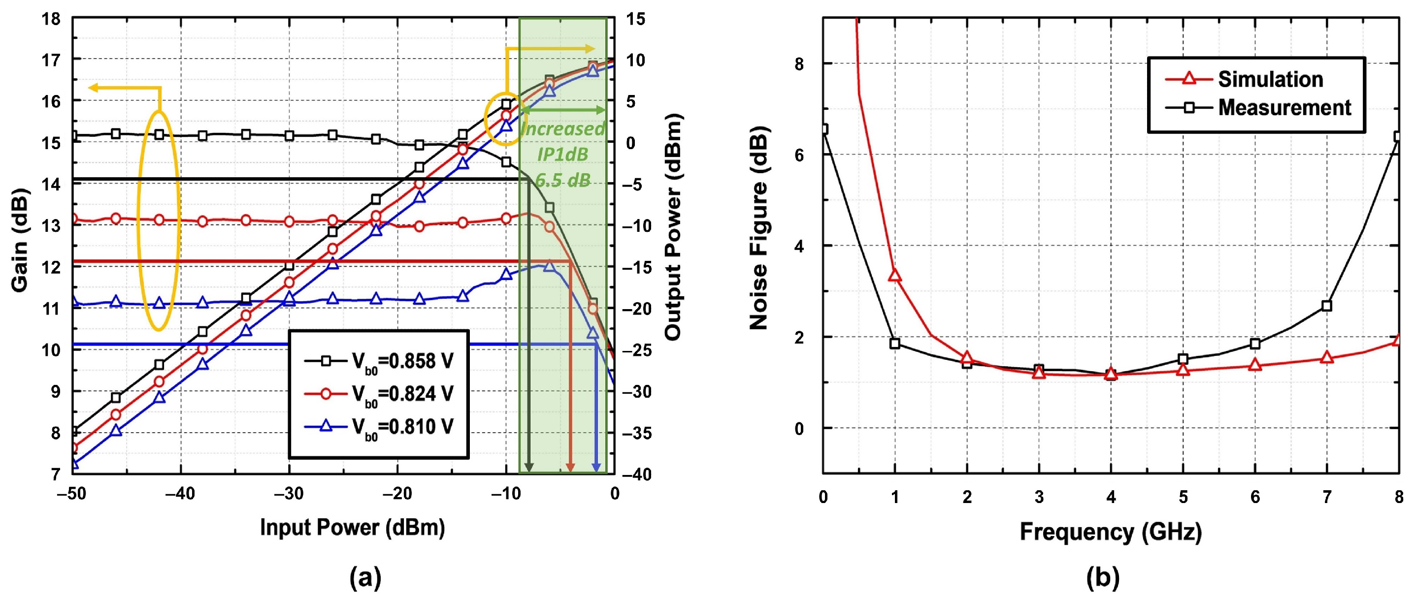
Finally, the IP1dB gain of the proposed VGLNA is determined by the steps described in Figure 7 with a measured range of shown in Figure 10b thanks to a fixed-bias prototype. The operation of three gain modes with respect to three different is shown in Figure 11a. It can be seen that IP1dB is −8 dBm, −4 dBm and −1.5 dBm with of 858 mV, 824 mV, and 810 mV, respectively, and it is confirmed that VGLNA using the ADB circuit operates with an extended IP1dB of 6.5 dB as compared to a counterpart with fixed of 858 mV.

Figure 11.
(a) IP1dB gain based on fixed-bias circuit operations, (b) measured noise figure.
4.3. Noise Figure
The noise figure is a very important aspect when assess an LNA design. In addition of JFET and the diode components, the noise figure performance of the proposed design is apparently degraded as compared to the single-BJT LNA. Applying the same supplying voltages, the VGLNA exhibits a measured NF of 1.8 dB at 6 GHz as shown in Figure 11b, which is in a good agreement with the simulated one. It is also noted that the lowest NF is not recorded at the target frequency because the input matching network is designed at the intermediate impedance in order to provide a good balance between NF and power performance.
5. Conclusions
In this paper, a variable-gain single-stage LNA is realized successfully for radar-detection applications, aiming at increasing the IP1dB of the high and fixed gain LNA one. The proposed LNA deploys a novel ADB circuit to produce a biasing voltage for BJT. This operation is automatic, providing a high gain at a low-power signal and a lower gain as the signal grows. The operation is verified, showing that IP1dB is extended by 6 dB as the input power increases from dBm to 0 dBm. Compared to the common fixed gain LNA, the proposed VGLNA has the clear advantage of not only achieving a high gain at a low-power signal but having a wider linear processing region. With this ADB deployment, the VGLNA exhibits a compact size of mm × mm and a low NF of dB, which is suitable for practical radar applications. A comparison among the state-of-the-art designs is summarized in Table 2. For an accurate comparison, three figures of merit (FOMs) are used as defined in Equations (12)–(14), which are presented [18]. The proposed VGLNA has the highest FOM2 and FOM3.
Table 2.
Performance comparison with other state-of-the-art works.
Author Contributions
Conceptualization, H.N., D.-A.N. and Y.K.; methodology, H.N. and D.-A.N.; software, H.N. and D.-A.N.; validation, H.N., Y.K., D.-A.N. and C.S.; formal analysis, D.-A.N. and Y.K.; investigation, H.N., D.-A.N. and Y.K. resources, C.S.; data curation, H.N. and Y.K.; writing—original draft preparation, H.N., D.-A.N. and Y.K. writing—review and editing, Y.K. and C.S.; visualization, H.N. and D.-A.N.; supervision, Y.K. and C.S.; project administration, Y.K. and C.S.; funding acquisition, C.S. All authors have read and agreed to the published version of the manuscript.
Funding
This work was supported by the National Research Foundation of Korea (NRF) Grant funded by the Korea government (Ministry of Science and ICT (MSIT)) under Grant 2017R1A5A1015596.
Conflicts of Interest
The authors declare no conflict of interest.
References
- Skolnik, M.I. Introduction to Radar System; McGraw-Hill Education: New York, NY, USA, 2002. [Google Scholar]
- Lacomme, P.; Marchais, J.C.; Hardange, J.P.; Normant, E. Air and Spaceborne Radar Systems; An Introduction; SPIE: Philadelphia, PA, USA, 2001. [Google Scholar]
- Kuo, W.-M.; Liang, Q.; Cressler, J.D.; Mitchell, M.A. An X-band SiGe LNA with 1.36 dB mean noise figure for monolithic phased array transmit/receive radar modules. In Proceedings of the IEEE Radio Frequency Integrated Circuits Symposium (RFIC), San Francisco, CA, USA, 11–13 June 2006. [Google Scholar]
- Chen, Z.; Zheng, T.; Luo, J. Octopus: A practical and versatile wideband MIMO sensing platform. In Proceedings of the 27th Annual International Conference on Mobile Computing and Networking (MobiCom), New Orleans, LA, USA, 25–29 October 2021. [Google Scholar]
- Ding, R.; Jin, H.; Xiang, D.; Wang, X.; Zhang, Y.; Shen, D.; Su, L.; Hao, W.; Tao, M.; Wang, L.; et al. Soil Moisture Sensing with UAV-Mounted IR-UWB Radar and Deep Learning. Proc. ACM Interact. Mob. Wearable Ubiquitous Technol. 2023, 7, 1–25. [Google Scholar] [CrossRef]
- Zhao, R.; Woodford, T.; Wei, T.; Qian, K.; Zhang, X. M-cube: A millimeter-wave massive MIMO software radio. In Proceedings of the 26th Annual International Conference on Mobile Computing and Networking (MobiCom), London, UK, 21–25 September 2020. [Google Scholar]
- Kuo, C.-C.; Tsai, Z.-M.; Tsai, J.-H.; Wang, H. A 71–76 GHz CMOS variable gain amplifier using current steering technique. In Proceedings of the IEEE Radio Frequency Integrated Circuits Symposium (RFIC), Atlanta, GA, USA, 15–17 June 2008. [Google Scholar]
- Kao, K.-Y.; Lu, D.-R.; Kao, J.-C.; Lin, K.-Y. A 60 GHz variable gain low-noise amplifier with low phase variation. In Proceedings of the International Symposium Radio-Frequency Integration Technology, Taipei, Taiwan, 24–26 August 2016. [Google Scholar]
- Liu, H.; Zhu, X.; Boon, C.C.; He, X. Cell-based variable-gain amplifiers with accurate dB-linear characteristic in 0.18 µm CMOS technology. IEEE J. Solid-State Circuits 2015, 50, 586–596. [Google Scholar] [CrossRef]
- Hsieh, Y.-K.; Kuo, J.-L.; Wang, H.; Lu, L.-H. A 60 GHz broadband low-noise amplifier with variable-gain control in 65 nm CMOS. IEEE Microw. Wirel. Compon. Lett. 2011, 21, 610–612. [Google Scholar] [CrossRef]
- Min, B.-W.; Rebeiz, G.M. Ka-Band SiGe HBT low phase imbalance differential 3-bit variable gain LNA. IEEE Microw. Wirel. Compon. Lett. 2008, 18, 272–274. [Google Scholar] [CrossRef]
- Jang, J.; Oh, J.; Kim, C.; Hong, S. A 79-GHz adaptive–gain and low noise UWB radar receiver front-end in 65-nm CMOS. IEEE Trans. Microw. Theory Technol. 2016, 64, 859–867. [Google Scholar] [CrossRef]
- Liu, C.; Yan, Y.-P.; Goh, W.-L.; Xiong, Y.-Z.; Zhang, L.-J.; Madihian, M. A 5-Gb/s automatic gain control amplifier with temperature compensation. IEEE J. Solid-State Circuits 2012, 47, 1323–1333. [Google Scholar] [CrossRef]
- Vidkjaer, J. RF-Circuits; Class Notes for the Course: RF Communication; 2000. Available online: https://dokumen.tips/documents/rf-communication-2-chap5-power-and-nonlinear-rf-amplifiers-rf-communication.html?page=1 (accessed on 25 April 2023).
- Nguyen, D.-A.; Seo, C. A compact and high-efficiency design of 0.915/2.45 GHz dual-band shunt-diode rectifier for wireless power transfer. IEEE Microw. Wirel. Compon. Lett. 2022, 32, 915–918. [Google Scholar] [CrossRef]
- He, Z.; Lin, H.; Liu, C. A novel class-C rectifier with high efficiency for wireless power transmission. IEEE Microw. Wirel. Compon. Lett. 2020, 30, 1197–1200. [Google Scholar] [CrossRef]
- Floyd, T.L. Electronic Devices: Electron Flow Version, 9th ed.; Prentice Hall: Hoboken, NJ, USA, 2011. [Google Scholar]
- Linten, D.; Thijs, S.; Natarajan, M.I.; Wambacq, P.; Jeamsaksiri, W.; Ramos, J.; Mercha, A.; Jenei, S.; Donnay, S.; Decoutere, S. A 5-GHz fully integrated ESD-protected low-noise amplifier in 90-nm RF CMOS. IEEE J. Solid-State Circuits 2005, 40, 1434–1442. [Google Scholar] [CrossRef]
- Gao, H.; Li, N.; Li, M.; Wang, S.; Zhang, Z.; Kuan, Y.C.; Yu, X.; Gu, Q.J.; Xu, Z. A 6.5–12 GHz balanced variable gain low-noise amplifier with frequency-selective non-foster gain equalization technique. In Proceedings of the IEEE/MTT-S International Microwave Symposium, Los Angeles, CA, USA, 4–6 August 2020. [Google Scholar]


Disclaimer/Publisher’s Note: The statements, opinions and data contained in all publications are solely those of the individual author(s) and contributor(s) and not of MDPI and/or the editor(s). MDPI and/or the editor(s) disclaim responsibility for any injury to people or property resulting from any ideas, methods, instructions or products referred to in the content. |
© 2023 by the authors. Licensee MDPI, Basel, Switzerland. This article is an open access article distributed under the terms and conditions of the Creative Commons Attribution (CC BY) license (https://creativecommons.org/licenses/by/4.0/).