
A Miniaturized Bandpass Filter with Wideband and High Stopband Rejection Using LTCC Technology

Abstract
:1. Introduction
2. Filter Structure Design
2.1. Filter Principle
2.2. Filter Circuit Prototype
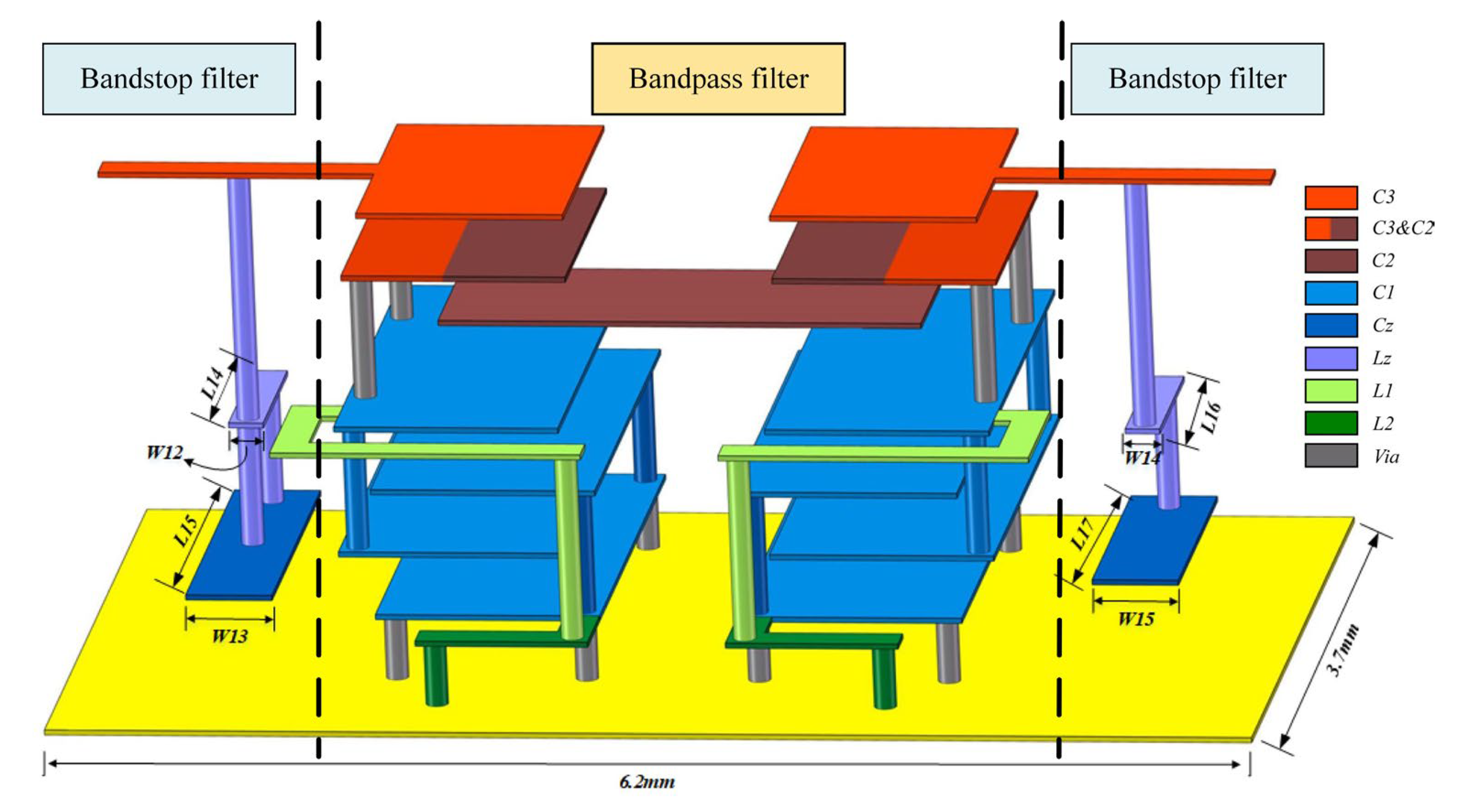
3. 3D Structural Design
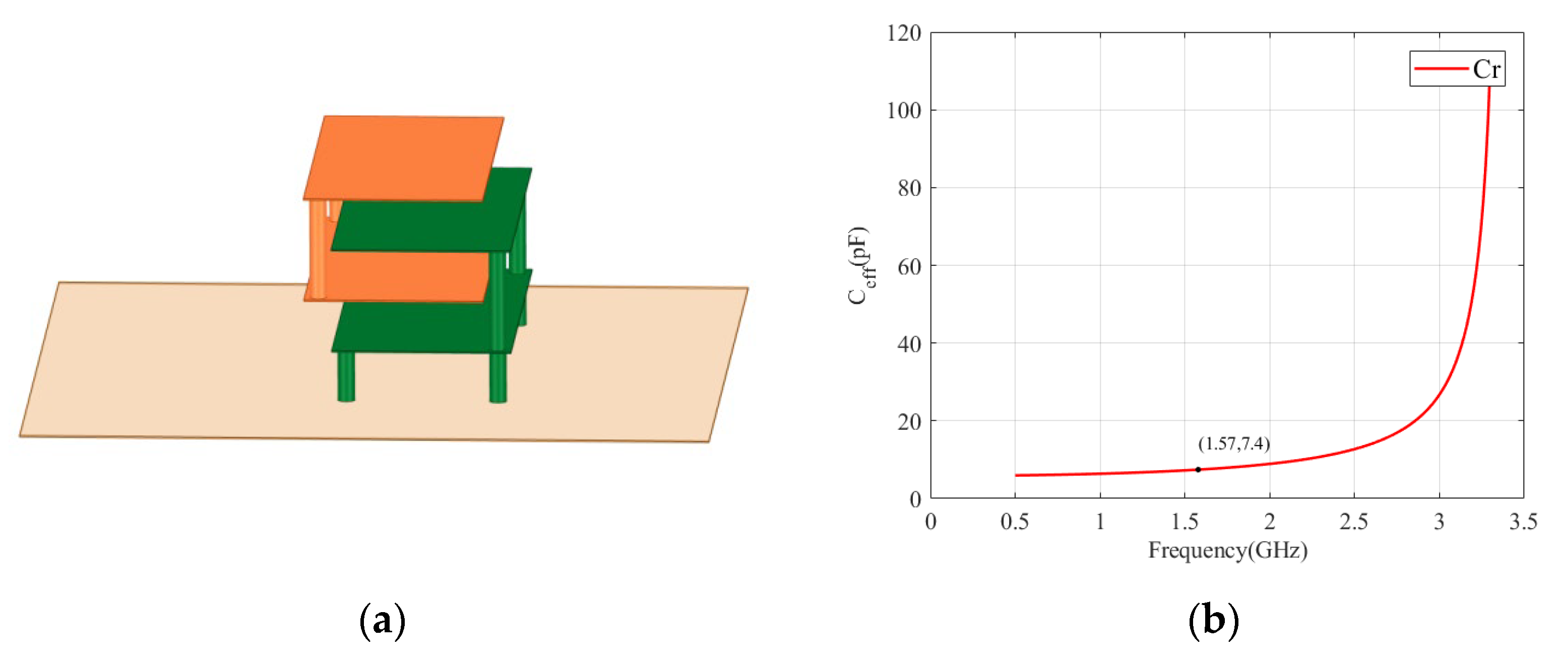
3.1. Capacitors
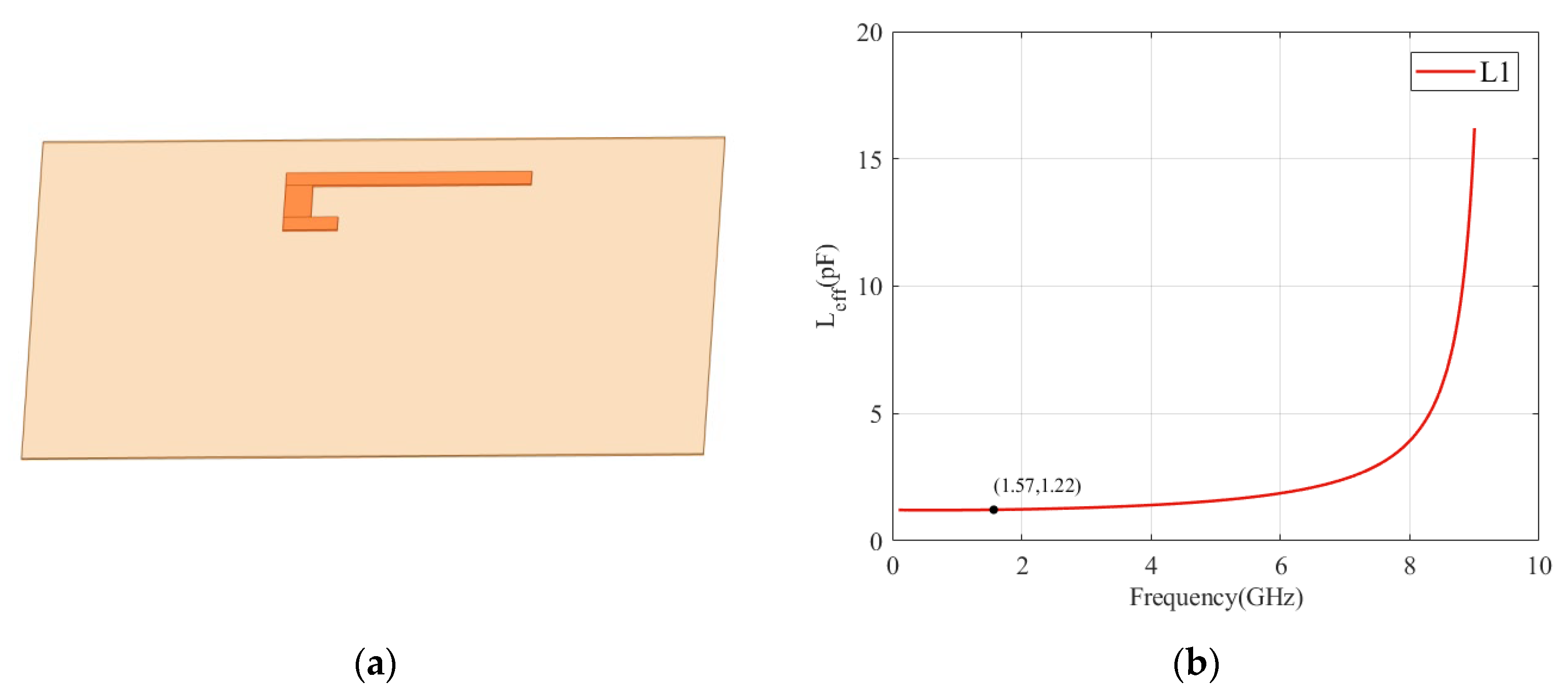
3.2. Inductors
3.3. Simulation Results
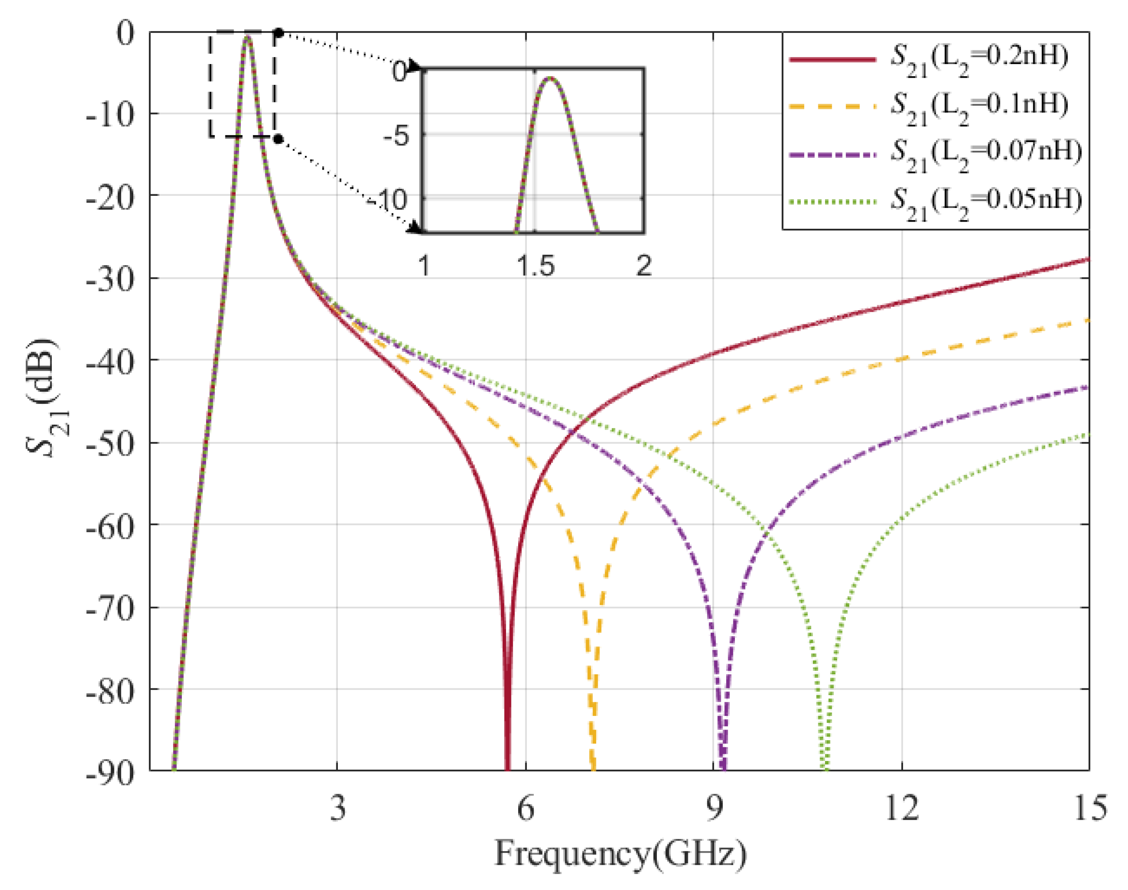
4. Wide Stopband Filter Design
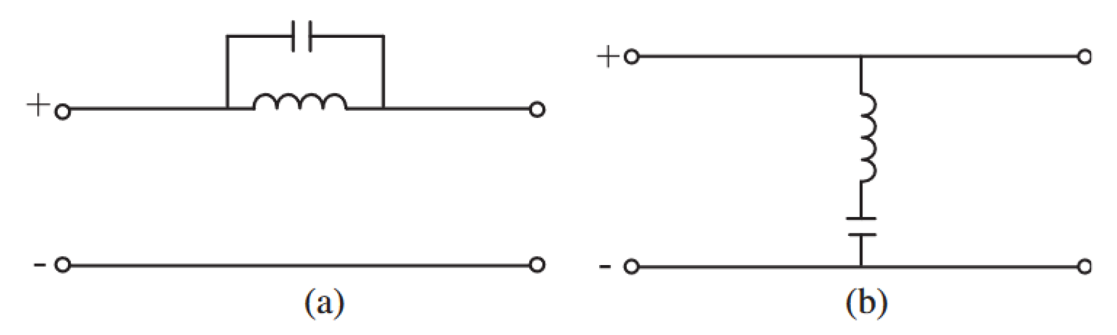
4.1. Principle of the Wide Stopband Filter
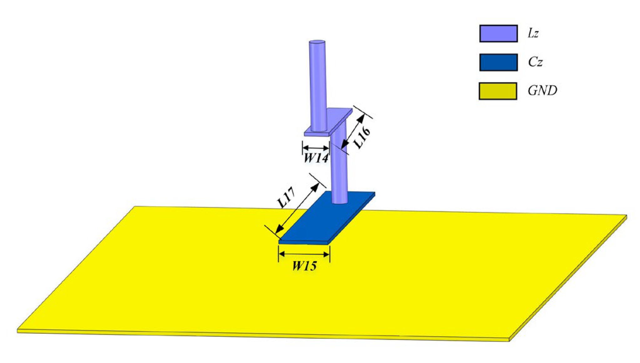
4.2. Three-Dimensional Structural Design
4.3. Simulation Results
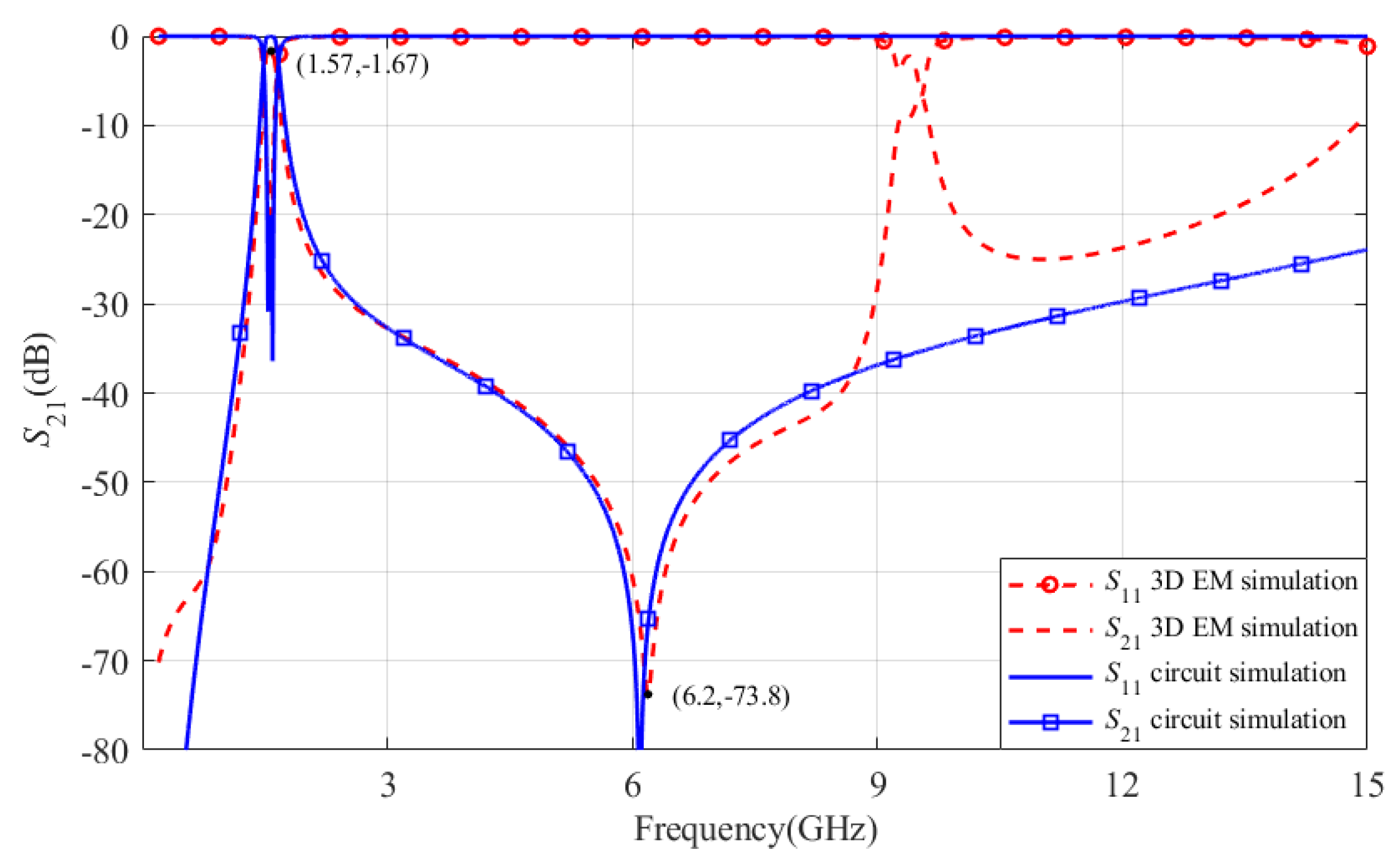
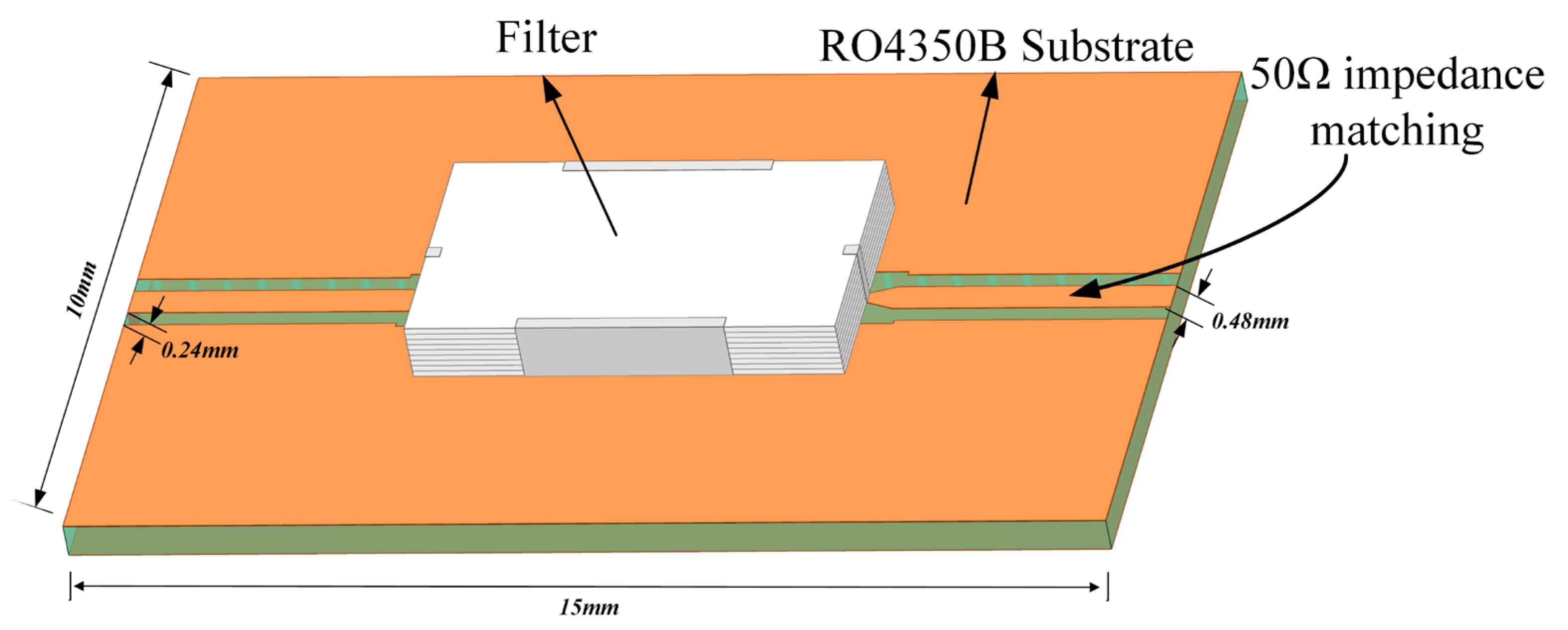
5. Overall Simulation
5.1. Simulation Results
5.2. Performance Comparison
6. Conclusions
Author Contributions
Funding
Data Availability Statement
Acknowledgments
Conflicts of Interest
References
- Ihle, M.; Ziesche, S.; Zech, C.; Baumann, B. Compact LTCC packaging and printing technologies for Sub–THz modules. In Proceedings of the 2018 7th Electronic System-Integration Technology Conference (ESTC), Dresden, Germany, 18–21 September 2018. [Google Scholar]
- Tang, J.M.; Liu, H.W.; Yang, Y. Balanced dual-band superconducting filter using stepped-impedance resonators with high band-to-band isolation and wide stopband. IEEE Trans. Circuits Syst. II Express Briefs 2021, 68, 131–135. [Google Scholar] [CrossRef]
- Xia, L.; Wu, B.; Song, L.; Chen, J.Z.; Cheng, Q.S. Design of pseudoelliptic filters with controllable transmission zeros using high-Q double-layer suspended stripline resonators. Int. J. RF Microw. Comput. Aided Eng. 2019, 29, e21785. [Google Scholar] [CrossRef]
- Xu, K.D.; Xu, H.; Liu, Y.H.; Ai, J.; Liu, Q.H. Short- and open-stub loaded spiral resonator and its application in planar microstrip filters. IET Microw. Antennas Propag. 2017, 11, 363–369. [Google Scholar] [CrossRef]
- Kim, C.H.; Chang, K. Wide-stopband bandpass filters using asymmetric stepped-impedance resonators. IEEE Microw. Wirel. Compon. Lett. 2013, 23, 69–71. [Google Scholar] [CrossRef]
- Arabi, E.; Lahti, M.; Vähä-Heikkilä, T.; Shamim, A. A 3-D miniaturized high selectivity bandpass filter in LTCC technology. IEEE Microw. Wirel. Compon. Lett. 2014, 24, 8–10. [Google Scholar] [CrossRef]
- Tan, C.; Yu, Z.J.; Xie, C.S. An L-band bandpass filter with narrow bandwidth and miniature based on LTCC technology. Prog. Electromagn. Res. 2019, 87, 63–72. [Google Scholar] [CrossRef]
- Peng, Z.; Zhou, J.; Rao, Y.B.; Deng, Z.X.; Luo, X. Compact bandpass filter with wide stopband and low radiation using fully-packaged substrate integrated defected ground structure. In Proceedings of the 2021 IEEE International Symposium on Radio-Frequency Integration Technology (RFIT), Hualien, Taiwan, 25–27 August 2021. [Google Scholar]
- Li, S.X.; Ma, K.X.; Chen, X.; Yan, N.N.; Fu, H.P. A miniaturized bandpass filter with wideband and high stopband rejection using LTCC technology. In Proceedings of the 2020 IEEE Asia-Pacific Microwave Conference (APMC), Hong Kong, China, 8–11 December 2020. [Google Scholar]
- Feng, W.J.; Gao, X.; Che, W.Q.; Yang, W.C.; Xue, Q. LTCC wideband bandpass filters with high performance using coupled lines with open/shorted stubs. IEEE Trans. Compon. Packaging Manuf. Technol. 2017, 7, 602–609. [Google Scholar] [CrossRef]
- Dai, Y.S.; Xu, L.; Han, Q.F.; Chen, S.B.; Wang, L.J.; Chen, R.Q. Miniaturized LTCC wideband bandpass filter using lumped-element shunt LC resonators. In Proceedings of the 2012 International Conference on Microwave and Millimeter Wave Technology (ICMMT), Shenzhen, China, 5–8 May 2012. [Google Scholar]
- Du, J.C.; Chen, N.; Lu, Q.Y. Design of a Ka-band Microstrip quasi-Yagi antenna array based on LTCC substrate. In Proceedings of the 2013 IEEE International Conference on Microwave Technology & Computational Electromagnetics, Qingdao, China, 25–28 August 2013. [Google Scholar]
- Matthaei, G.L.; Young, L.; Jones, E.M.T. Microwave Filters, Impedance-Matching Networks, and Coupling Structures; Artech House, Inc.: Boston, MA, USA, 1980. [Google Scholar]
- Hong, J.S.; Lancaster, M.J. Advanced RF/microwave filters. In Microstrip Filters for RF/Microwave Applications; Hong, J.S., Lancaster, M.J., Eds.; John Wiley & Sons, Ltd.: New York, NY, USA, 2001; pp. 315–377. [Google Scholar]
- Leung, W.Y.; Cheng, K.K.M.; Wu, K.L. Multilayer LTCC bandpass filter design with enhanced stopband characteristics. IEEE Microw. Wirel. Compon. Lett. 2002, 12, 240–242. [Google Scholar] [CrossRef]
- Wu, J.J.; Yan, B.; Zhang, Q.S.; Guo, G.F.; Su, H. Design and parameters extraction methods of microwave LTCC embedded inductor. Telecommun. Eng. 2007, 123–126. (In Chinese) [Google Scholar]
- Zhu, L.F. Narrowband LTCC filter with length-reduced end-coupled resonators. Prog. Electromagn. Res. Lett. 2020, 93, 13–19. [Google Scholar] [CrossRef]
- Dai, Y.S.; Zhang, H.S.; Qi, G.P.; Lu, D.L.; Tao, Z.L.; Qian, G.X.; Wang, H. LTCC bandpass filter for BluetoothTM application with dual transmission zeros. In Proceedings of the 2008 International Conference on Microwave and Millimeter Wave Technology, Nanjing, China, 21–24 April 2008. [Google Scholar]
- Cui, L.W.; Yu, J.G.; Li, S.L.; Liu, Y.N. A sharp-rejection dual-bandstop filter with multiple transmission poles and zeros based on transversal signal-interaction concepts. In Proceedings of the 2017 IEEE 5th International Symposium on Electromagnetic Compatibility (EMC-Beijing), Beijing, China, 28–31 October 2017. [Google Scholar]
- Barik, R.K.; Koziel, S.; Pietrenko-Dabrowska, A. Broad stopband, low-loss, and ultra-compact dual-mode bandpass filter based on HMSIRC. Electronics 2023, 12, 2831. [Google Scholar] [CrossRef]
- Li, Y.L.; Zhu, X.; Liu, J.C.; Zhou, L.J.; Wang, Z.H. Miniaturization of low temperature co-fired ceramic packaging for microwave filters. In Proceedings of the 2018 19th International Conference on Electronic Packaging Technology (ICEPT), Shanghai, China, 8–11 August 2018. [Google Scholar]
- Chen, L.; Yang, Z.H.; Ling, S.X.; Ding, D.W. Design of LTCC bandpass filter with broadband external suppression for 5G applications. In Proceedings of the 2023 International Conference on Microwave and Millimeter Wave Technology (ICMMT), Qingdao, China, 14–17 May 2023. [Google Scholar]
- Duraisamy, T.; Barik, R.K.; Cheng, Q.S.; Kamakshy, S.; Sholampettai Subramanian, K. Miniaturized SIW filter using D-shaped resonators with wide out-of-band rejection for 5G applications. J. Electromagn. Waves Appl. 2020, 34, 2397–2409. [Google Scholar] [CrossRef]
- Tie, H.Y.; Luo, L.; Song, Z.C.; Ma, Q.; Hu, S.W.; Zhou, B. Dual-mode LTCC filter with 4th-order harmonic suppression for 5G N78 applications. In Proceedings of the 2021 International Conference on Microwave and Millimeter Wave Technology (ICMMT), Nanjing, China, 23–26 May 2021. [Google Scholar]


| Feature | Value |
|---|---|
| 1 dB passband range | 1.52–1.62 GHz |
| Insertion loss | ≤1.65 dB |
| Out-of-band rejection | 6.2f0 ≥ 44 dB |
| Return loss | >30 dB |
| Dimension | 0.036λ × 0.022λ |
| Structural Form | MIM Capacitor | VIC Capacitor |
|---|---|---|
| Occupied area | Large | Small |
| Self-resonant frequency | Slightly low | High |
| Q value | Slightly lower | High |
| Number of layers required | less | Multi |
| Type | Structural Form | Occupied Area | Self-Resonant Frequency | Q Value | Number of Floors |
|---|---|---|---|---|---|
| Monolayer | Planar | Maximum | Lowest | Lowest | least |
| Displacement | Small | High | High | Medium | |
| Multilayer | Stacked | Medium | Medium | Medium | Medium |
| Spiral | Smallest | Highest | Highest | Most |
| Refs. | F0 (GHz) | FBW (%) | IL (dB) | Stopband Bandwidth | Rejection Level (dB) | ) | Selectivity Factor (%) |
|---|---|---|---|---|---|---|---|
| [20] | 0.835 | 15.8% | 0.41 | <20 dB | 0.16 ∗ 0.12 | 32.51@20 dB | |
| [21] | 5.5 | 18.2% | 2.46 | <32 dB | 0.058 ∗ 0.029 | 9.9@32 dB | |
| [22] | 0.75 | 12.8% | 0.6 | <20 dB | 0.014 ∗ 0.02 | 5.87@20 dB | |
| [23] | 6.11 | 8.96 | 1.07 | <22 dB | 0.153 ∗ 0.194 | 32.22@20 dB | |
| [24] | 3.5 | 22.9% | 0.5 | <18 dB | 0.09 ∗ 0.09 | 13.0@20 dB | |
| This work | 1.57 | 6.3% | 1.65 | <44 dB | 0.036 ∗ 0.022 | 110@20 dB | |
| 75.98@40 dB |
Disclaimer/Publisher’s Note: The statements, opinions and data contained in all publications are solely those of the individual author(s) and contributor(s) and not of MDPI and/or the editor(s). MDPI and/or the editor(s) disclaim responsibility for any injury to people or property resulting from any ideas, methods, instructions or products referred to in the content. |
© 2023 by the authors. Licensee MDPI, Basel, Switzerland. This article is an open access article distributed under the terms and conditions of the Creative Commons Attribution (CC BY) license (https://creativecommons.org/licenses/by/4.0/).
Share and Cite
Ma, Y.; Du, Q.; Zhang, W.; Liu, C.; Zhang, H. A Miniaturized Bandpass Filter with Wideband and High Stopband Rejection Using LTCC Technology. Electronics 2024, 13, 166. https://doi.org/10.3390/electronics13010166
Ma Y, Du Q, Zhang W, Liu C, Zhang H. A Miniaturized Bandpass Filter with Wideband and High Stopband Rejection Using LTCC Technology. Electronics. 2024; 13(1):166. https://doi.org/10.3390/electronics13010166
Chicago/Turabian StyleMa, Yue, Qifei Du, Wei Zhang, Cheng Liu, and Hao Zhang. 2024. "A Miniaturized Bandpass Filter with Wideband and High Stopband Rejection Using LTCC Technology" Electronics 13, no. 1: 166. https://doi.org/10.3390/electronics13010166