Author Contributions
Methodology, S.T. and D.S.; software, D.S., J.G. and C.V.I.; validation, D.P. and S.T.; formal analysis, D.S.; investigation, D.S. and C.V.I.; writing—original draft preparation, S.T.; writing—review and editing, D.P., D.S. and S.T.; visualization, D.S., D.P. and J.G.; supervision, D.P. All authors have read and agreed to the published version of the manuscript.
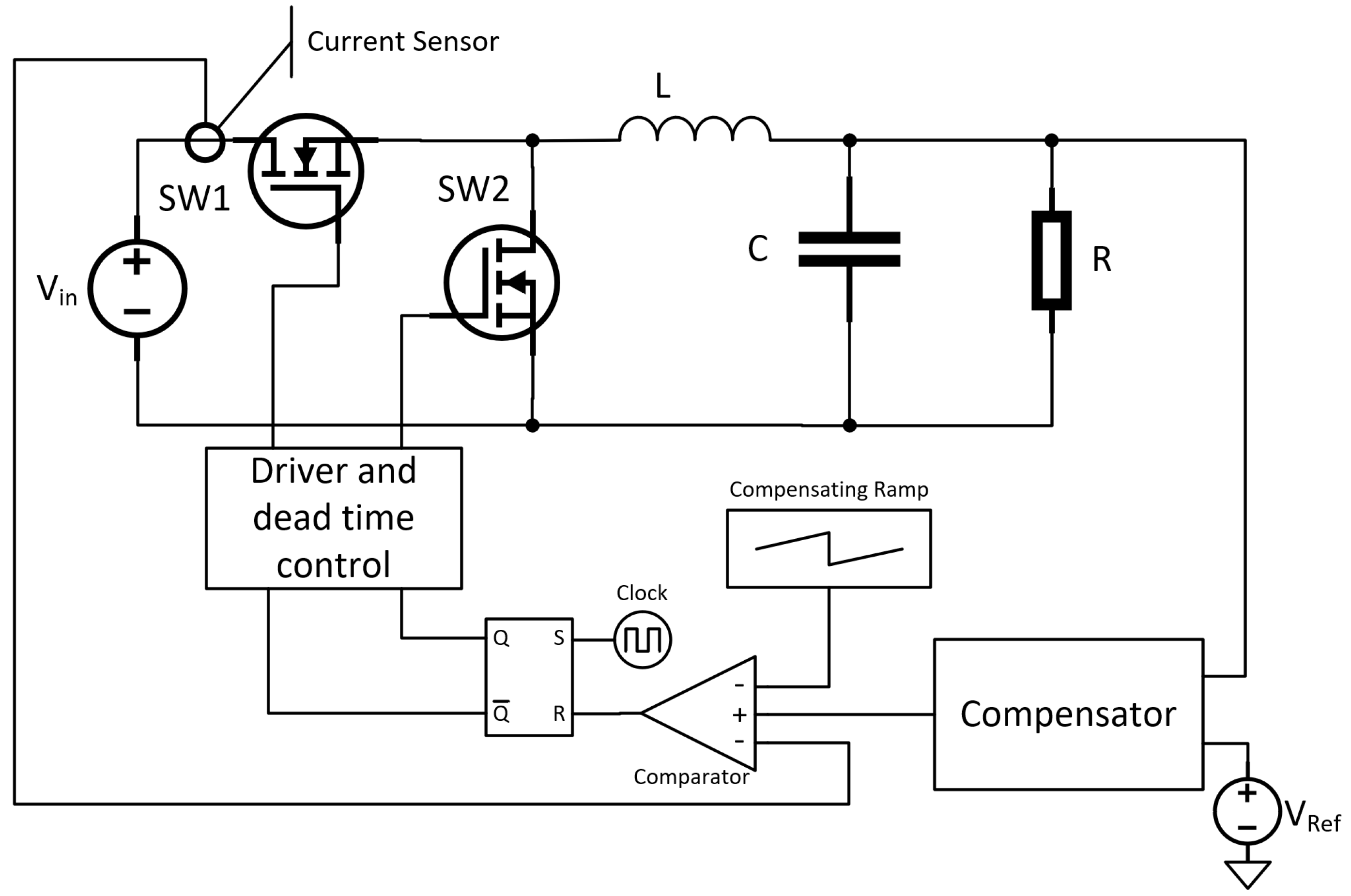
Figure 1.
Block diagram of the buck converter under peak-current-mode control.
Figure 1.
Block diagram of the buck converter under peak-current-mode control.
Figure 2.
Control signals of the buck converter under PCMC.
Figure 2.
Control signals of the buck converter under PCMC.
Figure 3.
The bifurcation map of the buck converter without compensation ramp. Vin = 6–12 V; Iref = 2–4 A; R = 2 Ω; L = 2.2 μH, C = 391 μF; f = 0.5 MHz, Sc = 0 V/s.
Figure 3.
The bifurcation map of the buck converter without compensation ramp. Vin = 6–12 V; Iref = 2–4 A; R = 2 Ω; L = 2.2 μH, C = 391 μF; f = 0.5 MHz, Sc = 0 V/s.
Figure 4.
The bifurcation diagrams for (a) Vin = 6 V and (b) Vin = 7 V (Iref = 2−4 A; R = 2 Ω; L = 2.2 μH, C = 391 μF; f = 0.5 MHz, Sc = 0 V/s). P1 stands for period-1 mode of operation, and P2 for period-2.
Figure 4.
The bifurcation diagrams for (a) Vin = 6 V and (b) Vin = 7 V (Iref = 2−4 A; R = 2 Ω; L = 2.2 μH, C = 391 μF; f = 0.5 MHz, Sc = 0 V/s). P1 stands for period-1 mode of operation, and P2 for period-2.
Figure 5.
Attractors for Vin = 6 V and (a) Iref = 3 A and (b) Iref = 3.5 A; for (a,b) R = 2 Ω; L = 2.2 μH, C = 391 μF; f = 0.5 MHz, Sc = 0 V/s.
Figure 5.
Attractors for Vin = 6 V and (a) Iref = 3 A and (b) Iref = 3.5 A; for (a,b) R = 2 Ω; L = 2.2 μH, C = 391 μF; f = 0.5 MHz, Sc = 0 V/s.
Figure 6.
The bifurcation map of the buck converter with compensation ramp. Vin = 6 V; Iref = 2–4 A; R = 2 Ω; L = 2.2 μH, C = 391 μF; f = 0.5 MHz, Sc = 0–2 × 10⁶ V/s.
Figure 6.
The bifurcation map of the buck converter with compensation ramp. Vin = 6 V; Iref = 2–4 A; R = 2 Ω; L = 2.2 μH, C = 391 μF; f = 0.5 MHz, Sc = 0–2 × 10⁶ V/s.
Figure 7.
The bifurcation diagrams for Sc = 0.2 × 10⁻⁶ V/s and Sc = 1 × 10⁶ V/s. Vin = 6 V; Iref = 2–4 A; R = 2 Ω; L = 2.2 μH, C = 391 μF; f = 0.5 MHz. P1 stands for period-1 mode of operation, P2 for period-2.
Figure 7.
The bifurcation diagrams for Sc = 0.2 × 10⁻⁶ V/s and Sc = 1 × 10⁶ V/s. Vin = 6 V; Iref = 2–4 A; R = 2 Ω; L = 2.2 μH, C = 391 μF; f = 0.5 MHz. P1 stands for period-1 mode of operation, P2 for period-2.
Figure 8.
The bifurcation diagram for Iref = 3.4 A. Vin = 6 V; R = 2 Ω; L = 2.2 μH, C = 391 μF; f = 0.5 MHz, Sc = 0–2 × 10⁶ V/s. P1 stands for period-1 mode of operation, and P2 for period-2.
Figure 8.
The bifurcation diagram for Iref = 3.4 A. Vin = 6 V; R = 2 Ω; L = 2.2 μH, C = 391 μF; f = 0.5 MHz, Sc = 0–2 × 10⁶ V/s. P1 stands for period-1 mode of operation, and P2 for period-2.
Figure 9.
CIP Hybrid Power Starter kit in peak-current-mode control configuration.
Figure 9.
CIP Hybrid Power Starter kit in peak-current-mode control configuration.
Figure 10.
Output voltage ripple measurement setup.
Figure 10.
Output voltage ripple measurement setup.
Figure 11.
Phase plot and autocorrelation function of the output voltage ripple ().
Figure 11.
Phase plot and autocorrelation function of the output voltage ripple ().
Figure 12.
Phase plot and autocorrelation function of output voltage ripple ().
Figure 12.
Phase plot and autocorrelation function of output voltage ripple ().
Figure 13.
Phase plot and autocorrelation function of output voltage ripple ().
Figure 13.
Phase plot and autocorrelation function of output voltage ripple ().
Figure 14.
Phase plot and autocorrelation function of output voltage ripple ().
Figure 14.
Phase plot and autocorrelation function of output voltage ripple ().
Figure 15.
Efficiency measurement setup.
Figure 15.
Efficiency measurement setup.
Figure 16.
The dependence of output voltage ripples on changes.
Figure 16.
The dependence of output voltage ripples on changes.
Figure 17.
The dependence of output voltage ripples on variation.
Figure 17.
The dependence of output voltage ripples on variation.
Figure 18.
Efficiency dependence on changes.
Figure 18.
Efficiency dependence on changes.
Figure 19.
Efficiency dependence on changes.
Figure 19.
Efficiency dependence on changes.
Table 1.
Parameters of the buck converter under test.
Table 1.
Parameters of the buck converter under test.
| Parameter | Values |
|---|
| Vin | 6…12 V |
| Iref | 2…4 A |
| R | 2 Ω |
| L | 2.2 μH |
| C | 391 μF |
| f | 0.5 MHz |
| Sc | 0 V/s |
Table 2.
The dependence of output voltage ripples on changes.
Table 2.
The dependence of output voltage ripples on changes.
| Mean Output Voltage Ripples | |
|---|
| Vref (V)↓ | Vin = 6 V | Vin = 8 V | Vin = 10 V | Vin = 12 V | Period-1 |
| 2 | 3.90 | 4.10 | 4.32 | 9.42 | Period-2 |
| 2.1 | 4.03 | 4.38 | 4.35 | 10.51 | Period-4 |
| 2.2 | 4.41 | 4.68 | 4.80 | 4.28 | Period-N |
| 2.3 | 8.71 | 5.04 | 5.17 | 4.51 | Chaos |
| 2.4 | 8.71 | 5.36 | 5.59 | 5.03 | Uncertain regime |
| 2.5 | 10.60 | 5.77 | 5.96 | 5.55 | |
| 2.6 | 12.05 | 5.97 | 6.33 | 5.99 | |
| 2.7 | 15.95 | 6.37 | 6.78 | 6.48 | |
| 2.8 | 16.46 | 6.59 | 7.21 | 6.86 | |
| 2.9 | 18.07 | 6.98 | 7.66 | 7.50 | |
| 3 | 21.56 | 11.19 | 8.10 | 7.83 | |
| 3.1 | 20.78 | 12.75 | 8.62 | 8.41 | |
| 3.2 | 23.19 | 12.76 | 9.01 | 8.88 | |
| 3.3 | 25.22 | 15.62 | 9.45 | 9.46 | |
| 3.4 | 27.17 | 17.33 | 9.91 | 10.00 | |
| 3.5 | 28.73 | 19.87 | 10.29 | 10.57 | |
Table 3.
The dependence of output voltage ripples on changes.
Table 3.
The dependence of output voltage ripples on changes.
| Vref Values (V) → | Mean Ripple Voltage Amplitude (Peak to Peak) for Parameters Rload − Vref (mV) | |
|---|
| Rload Values (Ω) → | 2 | 4 | 6 | 8 | 10 | |
|---|
| 2.5 | 3.83 | 2.97 | 3.07 | 2.84 | 2.91 | Period-1 |
| 2.9 | 4.83 | 3.85 | 2.90 | 3.63 | 3.60 | Period-2 |
| 3 | 11.36 | 4.16 | 3.94 | 3.84 | 4.13 | Period-N |
| 3.1 | 12.72 | 8.18 | 4.25 | 4.09 | 4.34 | Chaos |
| 3.2 | 13.20 | 12.92 | 4.38 | 4.30 | 4.50 | Uncertain regime |
| 3.3 | 15.70 | 12.64 | 22.21 | 30.49 | 4.87 | |
| 3.4 | 18.32 | 12.75 | 12.97 | 12.99 | 4.99 | |
| 3.5 | 19.08 | 12.64 | 13.07 | 12.84 | 13.06 | |
| 3.6 | 20.09 | 19.15 | 12.62 | 12.72 | 12.96 | |
| 3.7 | 25.86 | 21.74 | 12.71 | 12.72 | 12.76 | |
| 3.8 | 28.98 | 25.89 | 12.54 | 12.43 | 12.71 | |
Table 4.
Measurements data comparison to numerical analysis results.
Table 4.
Measurements data comparison to numerical analysis results.
| Vin = 6 V |
| Vref, V | Iref, A | Num. analysis mode |
| 2 | 2.13 | Period-1 |
| 2.4 | 2.82 | Period-2 |
| 2.7 | 3.02 | Period-N (Group 0) |
| 3.5 | 3.38 | Chaos |
| Vin = 8 V |
| Vref, V | Iref, A | Num. analysis mode |
| 2.5 | 2.70 | Period-1 |
| 3.2 | 3.72 | Period-2 |
| 3.5 | 3.93 | Period-N (Group 0) |
| 3.8 | 4.47 | Chaos |
| Vin = 10 V |
| Vref, V | Iref, A | Num. analysis mode |
| 2.2 | 2.51 | Period-1 |
| 2.6 | 2.92 | Period-1 |
| 3 | 3.29 | Period-1 |
| 3.5 | 3.72 | Period-2 |
Table 5.
Efficiency comparison for chaotic (PRG turned off) and period-1 (PRG turned on) modes ( group).
Table 5.
Efficiency comparison for chaotic (PRG turned off) and period-1 (PRG turned on) modes ( group).
| | , Ω | , V | , A | , V | , A | , V | η, % | η, % (PRG Turned Off) |
|---|
| With PRG turned on | 2 | 3.8 | 1.804 | 7.7172 | 2.593 | 5.0219 | 93.535% | 92.330% |
| 4 | 3.8 | 1.022 | 7.844 | 1.461 | 5.0175 | 91.443% | 89.077% |
Table 6.
Efficiency comparison for chaotic (PRG turned off) and period-1 (PRG turned on) modes ( group).
Table 6.
Efficiency comparison for chaotic (PRG turned off) and period-1 (PRG turned on) modes ( group).
| | , Ω | , V | , A | , V | , A | , V | η, % | η, % (PRG Turned Off) |
|---|
| With PRG turned on | 2 | 3.5 | 2.055 | 5.6817 | 2.385 | 4.6126 | 94.220% | 94.021% |
| 2 | 3.8 | 1.804 | 7.7172 | 2.593 | 5.0219 | 93.535% | 92.330% |


 ,
, 


