
Interface Contact Thermal Resistance of Die Attach in High-Power Laser Diode Packages

 ,
,  ,
,
Abstract
:1. Introduction
2. Materials and Methods
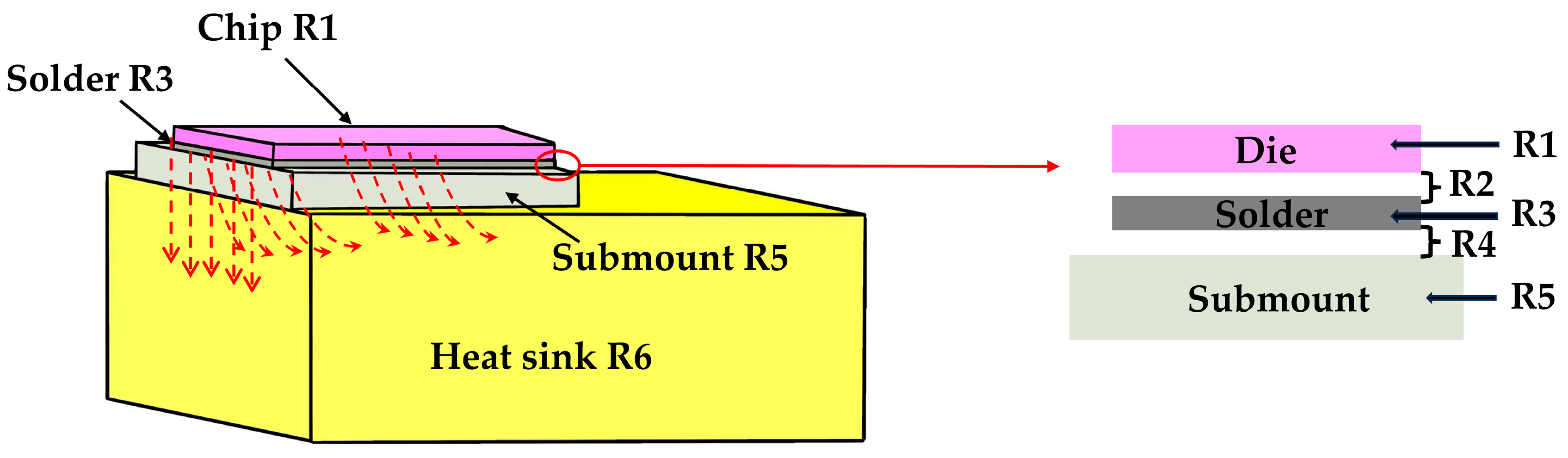
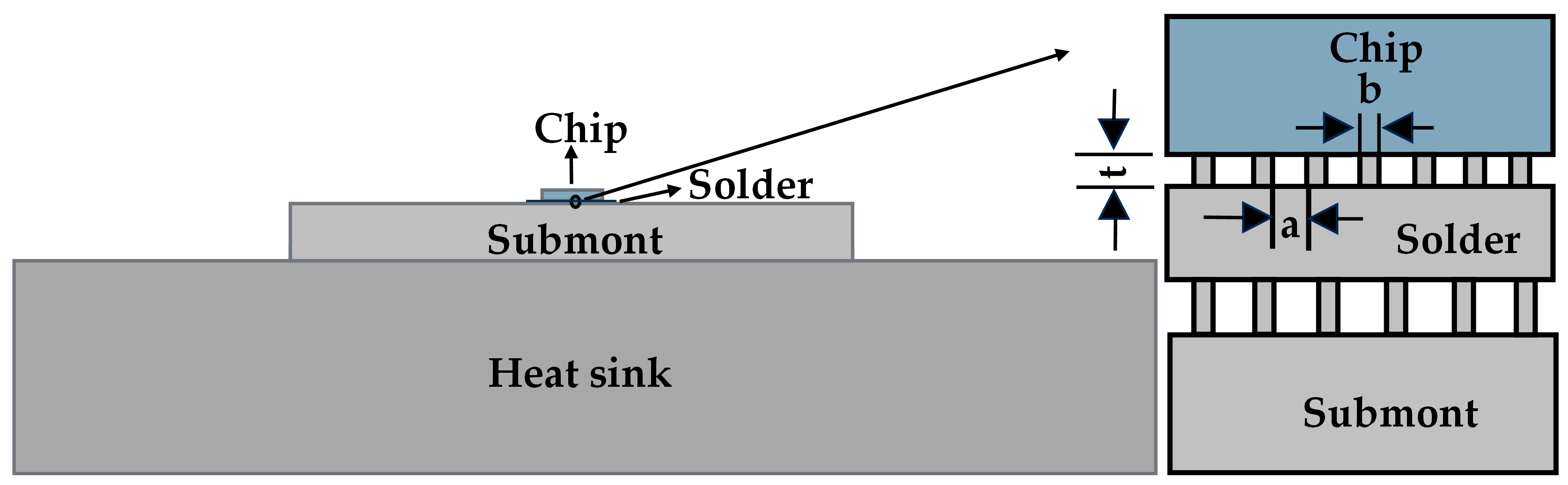
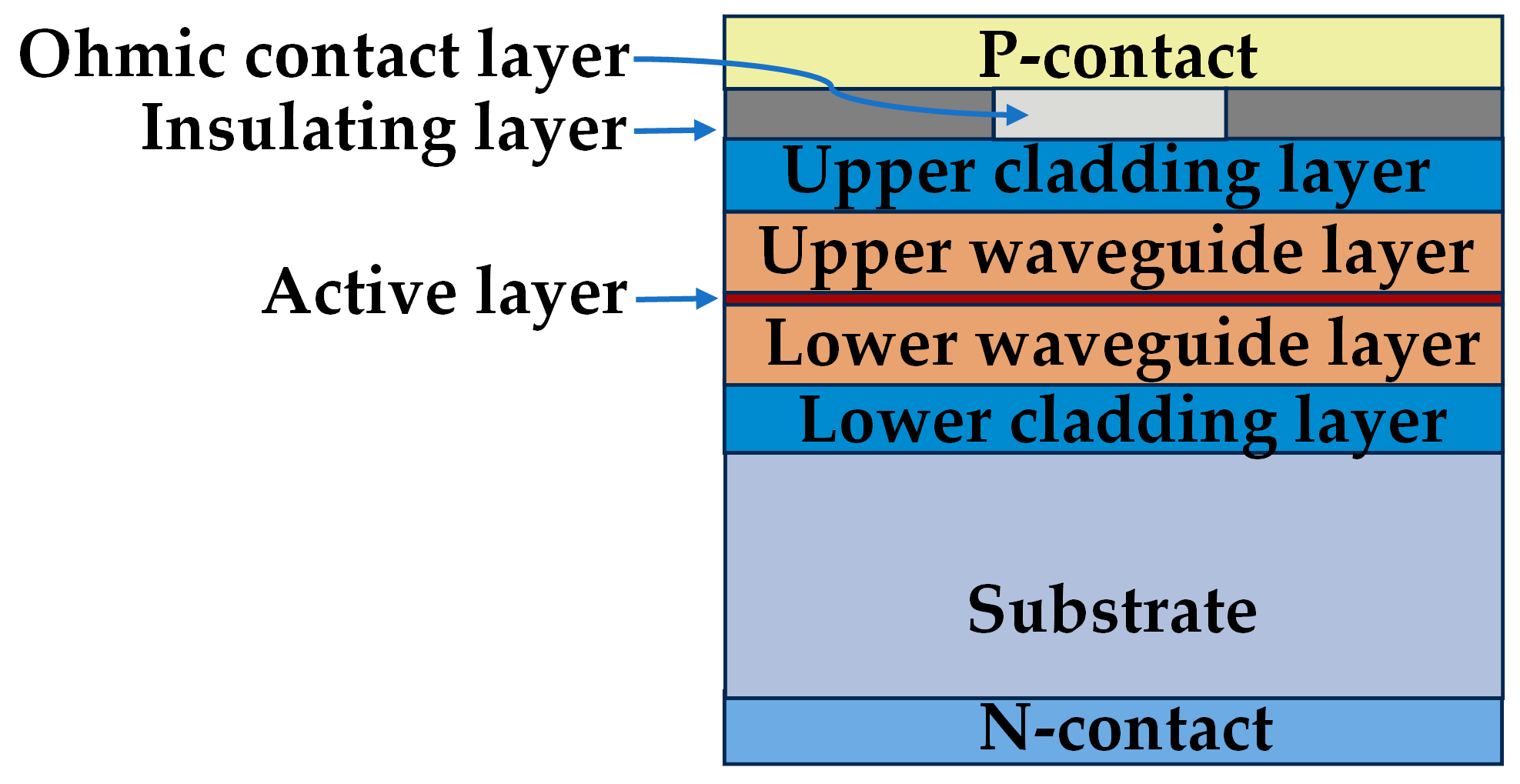
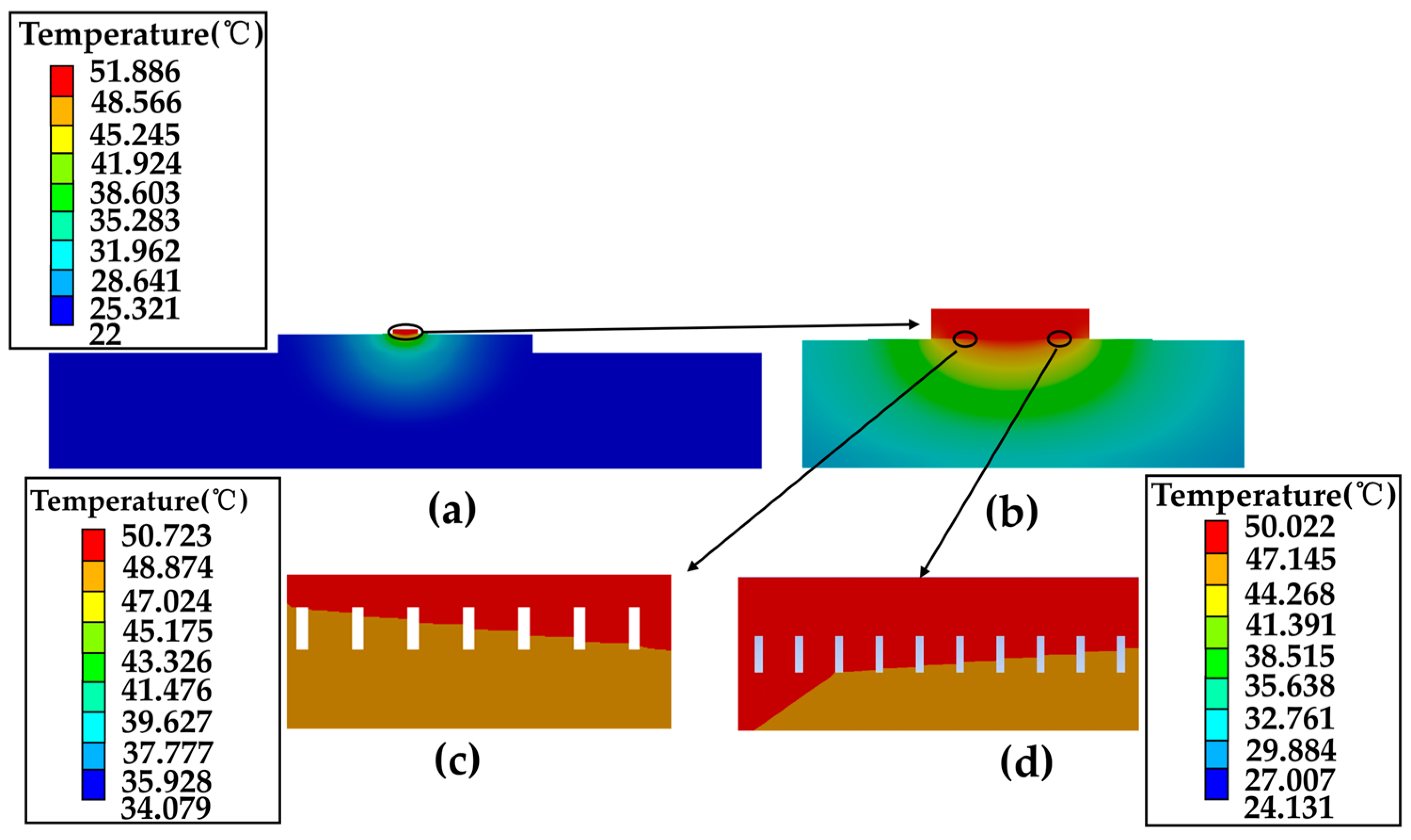
2.1. Simulation of F-Mount Packaged Single Emitter
2.2. Experiment of F-Mount Packaged Single Emitter
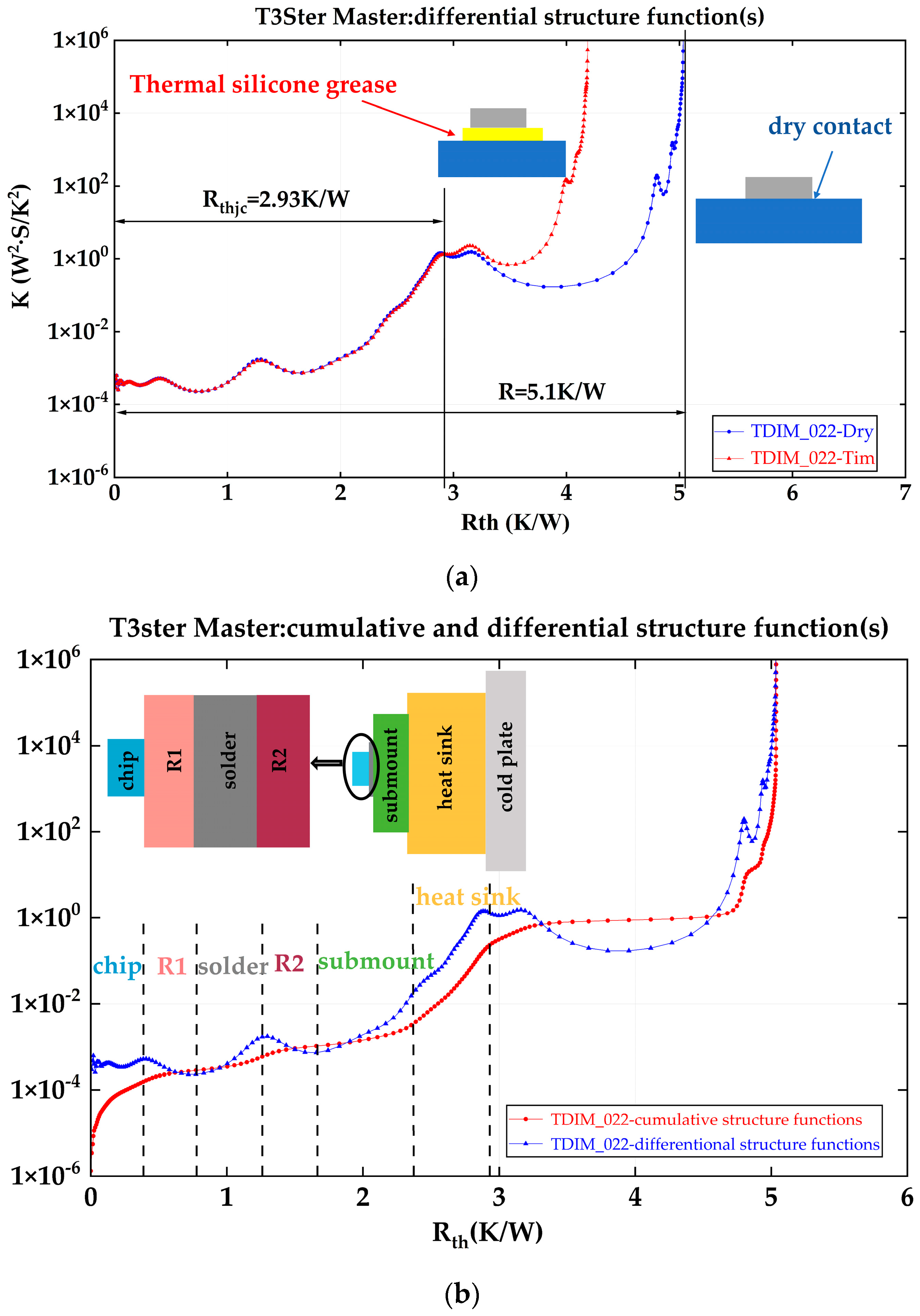
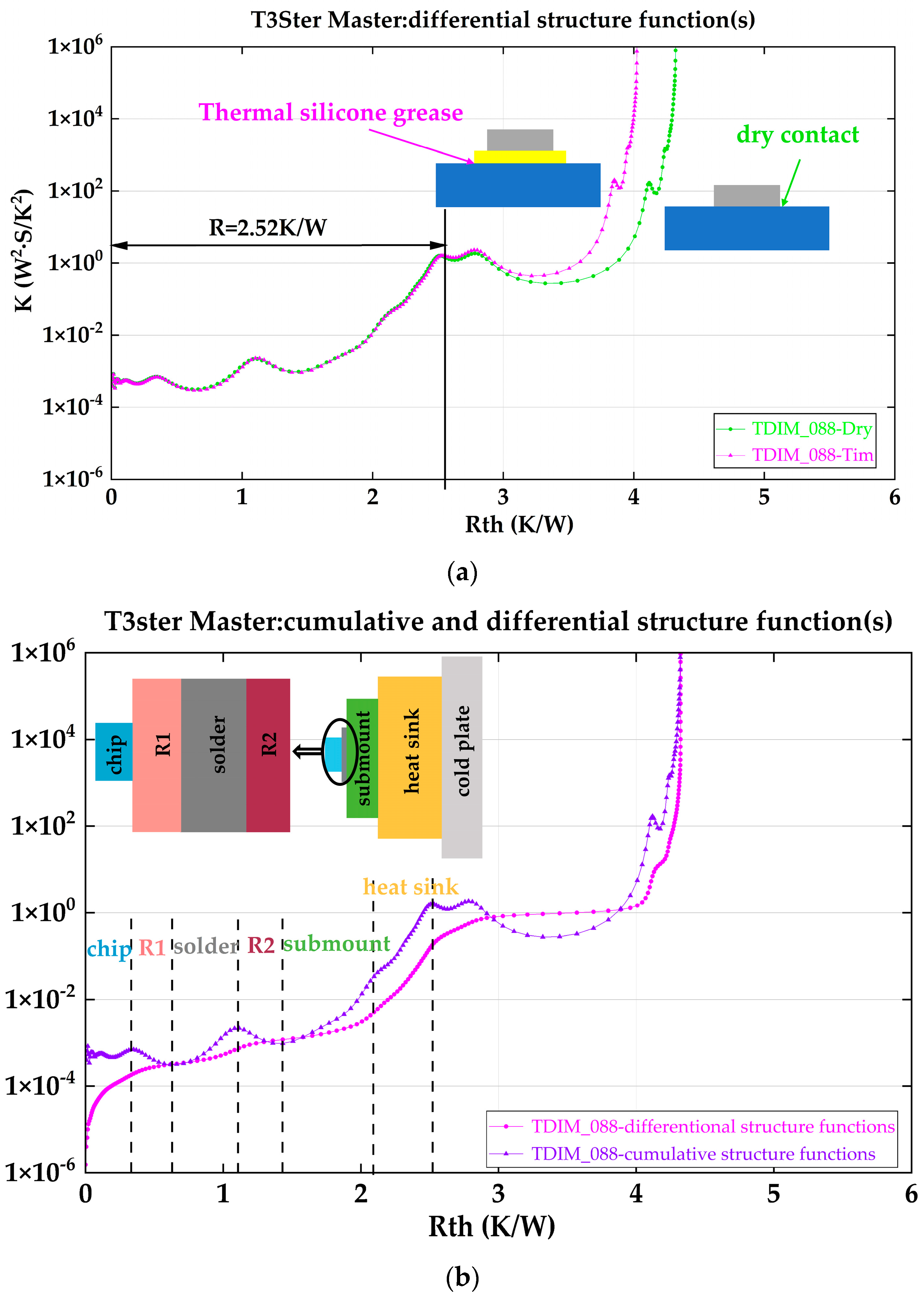
2.2.1. T3ster Interface Contact Thermal Resistance Testing
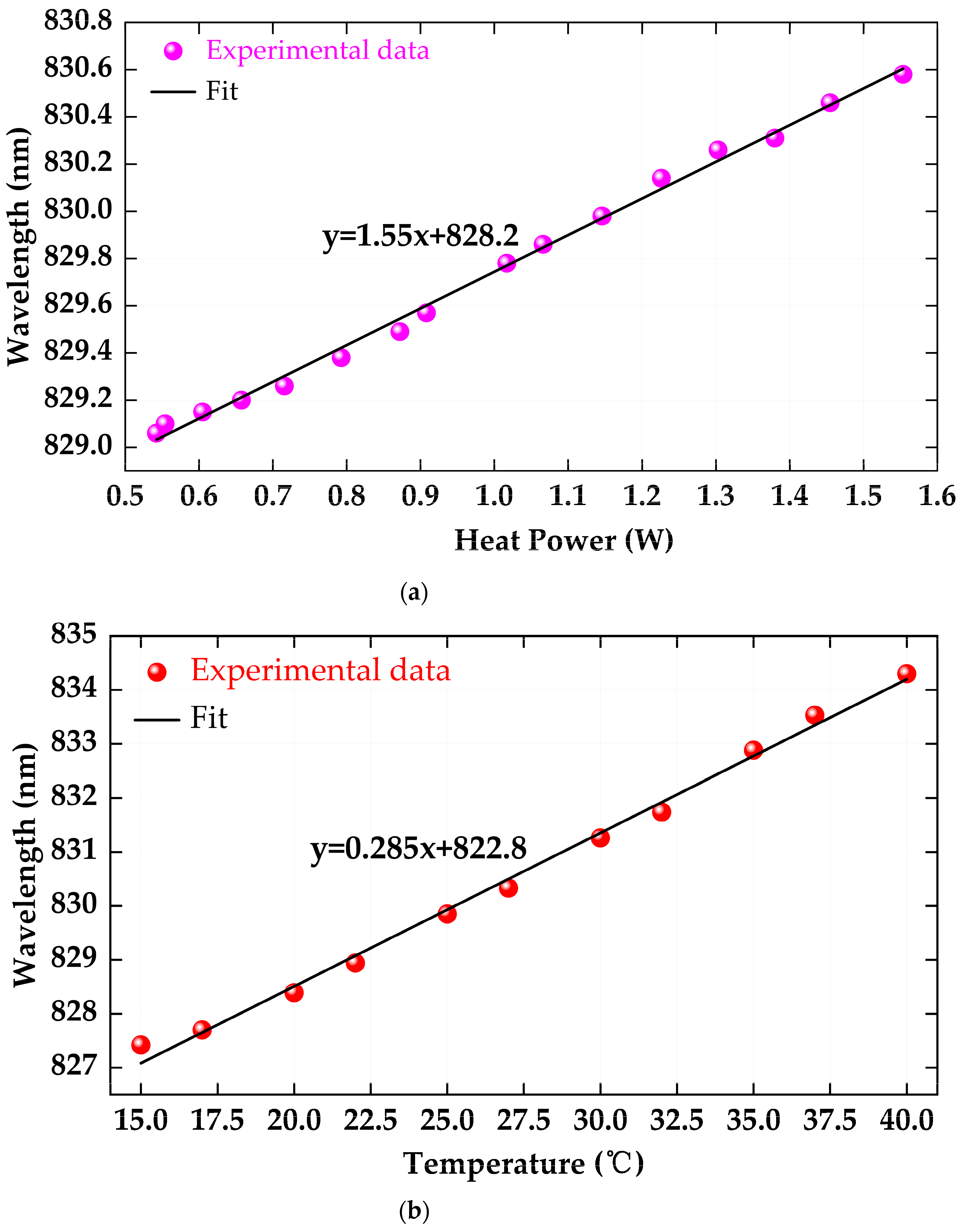
2.2.2. CW Power-Averaged Wavelength Measurement of the Overall Thermal Resistance
3. Results
3.1. Simulation of the Interface Contact Thermal Resistance
3.2. T3ster Interface Contact Thermal Resistance Testing
3.3. CW Power-Averaged Wavelength Measurement of the Overall Thermal Resistance
4. Discussion
5. Conclusions
Author Contributions
Funding
Data Availability Statement
Acknowledgments
Conflicts of Interest
References
- Faircloth, B. High-brightness high-power fiber coupled diode laser system for material processing and laser pumping. In Proceedings of the Conference on High-Power Diode Laser Technology and Applications, San Jose, CA, USA, 27–28 January 2003; pp. 34–41. [Google Scholar]
- Singh, A.; Mukhopadhyay, P.K.; Sharma, S.K.; Ranganathan, K.; Oak, S.M. 82 W Continuous-Wave Green Beam Generation by Intracavity Frequency Doubling of Diode-Side-Pumped Nd:YAG Laser. IEEE J. Quantum Electron. 2011, 47, 398–405. [Google Scholar] [CrossRef]
- Bailey, C.; IEEE. Thermal Management Technologies for Electronic Packaging: Current Capabilities and Future Challenges for Modelling Tools. In Proceedings of the 10th Electronics Packing Technology Conference, Singapore, 9–12 December 2008; pp. 527–532. [Google Scholar]
- He, Z.Q.; Yan, Y.F.; Zhang, Z.E. Thermal management and temperature uniformity enhancement of electronic devices by micro heat sinks: A review. Energy 2021, 216, 119223. [Google Scholar] [CrossRef]
- Kang, T.; Ye, Y.; Jia, Y.; Kong, Y.; Jiao, B. Enhanced Thermal Management of GaN Power Amplifier Electronics with Micro-Pin Fin Heat Sinks. Electronics 2020, 9, 1778. [Google Scholar] [CrossRef]
- Wipiejewski, T.; Peters, M.G.; Young, D.B.; Thibeault, B.J.; Fish, G.A.; Coldren, L.A. Thermal resistance of etched-pillar vertical-cavity surface-emitting laser diodes. In Proceedings of the Conference on Optoelectronic Packaging, San Jose, CA, USA, 1–2 February 1996; pp. 171–182. [Google Scholar]
- Chang, J.; Wang, L.; Dirk, J.; Xie, X. Finite element modeling predicts the effects of voids on thermal shock reliability and thermal resistance of power device. Weld. J. 2006, 85, 63S–70S. [Google Scholar]
- Kuc, M.; Wasiak, M.; Sarzaa, R.P. Impact of Heat Spreaders on Thermal Performance of III-N-Based Laser Diode. IEEE Trans. Compon. Packag. Manuf. Technol. 2015, 5, 474–482. [Google Scholar] [CrossRef]
- Otiaba, K.C.; Bhatti, R.S.; Ekere, N.N.; Mallik, S.; Alam, M.O.; Amalu, E.H.; Ekpu, M. Numerical study on thermal impacts of different void patterns on performance of chip-scale packaged power device. Microelectron. Reliab. 2012, 52, 1409–1419. [Google Scholar] [CrossRef]
- Ma, X.; Huo, J.; Qu, Y.; Du, S.; Wang, Y. Thermal-resistor Analysis of The Laser Chips with Different Size in C-mount Package. Chin. J. Lumin. 2011, 32, 184–187. [Google Scholar]
- Ni, Y.; Jing, H.; Kong, J.; Wang, C.; Liu, S.; Ma, X. Thermal Performance of High-Power Laser Diodes Packaged by SiC Ceramic Submount. Chin. J. Lasers 2018, 45, 0101002. [Google Scholar]
- Nishiguchi, M.; Goto, N.; Nishizawa, H. Highly reliable au-sn eutectic bonding with background gaas lsi chips. IEEE Trans. Compon. Hybrids Manuf. Technol. 1991, 14, 523–528. [Google Scholar] [CrossRef]
- Liu, D.; Wang, F.; Zeng, F.; Shang, X. Finite element simulation method of high temperature thermal contact resistance. Eng. Mech. 2012, 29, 375–379. [Google Scholar]
- Lu, Y.; Nie, Z.Q.; Zhang, P.; Wang, Z.F.; Xiong, L.L.; Wang, S.N.; Wu, D.H.; Liu, X.S. Numerical Simulation of Thermo-mechanical Behavior in High Power Diode Laser Arrays. In Proceedings of the 17th International Conference on Electronic Packaging Technology (ICEPT), Wuhan, China, 16–19 August 2016; Chinese Institute of Electronics: Portland, ME, USA; Electronic Manufacturing Company: Maplewood, NJ, USA; Packaging Technology Society: Wuhan, China, 2016; pp. 76–83. [Google Scholar]
- Ma, Z.; Lin, T.; Zhao, R.; Sun, W.; Mu, Y.; Li, Y.; Xie, J. Research on Thermal Analysis Modeling of Semiconductor Laser Based on Package Prototype. Laser Optoelectron. Prog. 2021, 58, 1450. [Google Scholar]
- Wang, S.; Bo, B.; Xu, L.; Du, Y.; Qiao, Z.; Gao, X. Thermal Analysis on Semiconductor Laser with Non-injection Region. Chin. J. Lumin. 2014, 35, 969–973. [Google Scholar] [CrossRef]
- Zhang, X.L.; Bo, B.X.; Qiao, Z.L.; Xu, Y.M.; Gao, X. Analysis of thermal characteristics based on a new type diode laser packaging structure. Opt. Eng. 2017, 56, 085105. [Google Scholar] [CrossRef]
- Romo, G.; Smy, T.; Walkey, D.; Reid, B. Modeling facet heating in ridge lasers. Microelectron. Reliab. 2003, 43, 99–110. [Google Scholar] [CrossRef]
- Ryvkin, B.S.; Avrutin, E.A. Free-carrier absorption and active layer heating in large optical cavity high-power diode lasers. J. Appl. Phys. 2006, 100, 2212147. [Google Scholar] [CrossRef]
- Wu, D.-H.; Zah, C.-E.; Liu, X. Three-dimensional thermal model of high-power semiconductor lasers. Appl. Opt. 2019, 58, 3892–3901. [Google Scholar] [CrossRef] [PubMed]
- Kim, D.S.; Holloway, C.; Han, B.; Bar-Cohen, A. Method for predicting junction temperature distribution in a high-power laser diode bar. Appl. Opt. 2016, 55, 7487–7496. [Google Scholar] [CrossRef] [PubMed]
- Xi, Y.; Schubert, E.F. Junction-temperature measurement in GaN ultraviolet light-emitting diodes using diode forward voltage method. Appl. Phys. Lett. 2004, 85, 2163–2165. [Google Scholar] [CrossRef]
- Liu, J.; Feng, S.W.; Zhang, G.C.; Zhu, H.; Guo, C.S.; Qiao, Y.B.; Li, J.W. A Novel Method for Measuring the Temperature in the Active Region of Semiconductor Modules. Chin. Phys. Lett. 2012, 29, 044401. [Google Scholar] [CrossRef]
- Yulin, G.A.O.; Yijun, L.V.; Zhong, C. Thermal Measurement of Power LED by Structure Function. Semicond. Optoelectron. 2008, 29, 329. [Google Scholar]
- Chen, Y.; Chen, M.; Gao, B.; Hu, B.; Lai, W.; Xu, S. Evaluation of Solder Failure of an IGBT Module Based on Transient Thermal Impedance. Proc. Chin. Soc. Electr. Eng. 2018, 38, 3059–3067. [Google Scholar]
- Anithambigai, P.; Shanmugan, S.; Mutharasu, D.; Zahner, T.; Lacey, D. Study on thermal performance of high power LED employing aluminum filled epoxy composite as thermal interface material. Microelectron. J. 2014, 45, 1726–1733. [Google Scholar] [CrossRef]
- Szekely, V. A new evaluation method of thermal transient measurement results. Microelectron. J. 1997, 28, 277–292. [Google Scholar] [CrossRef]
- Kim, H.H.; Choi, S.H.; Shin, S.H.; Lee, Y.K.; Choi, S.M.; Yi, S. Thermal transient characteristics of die attach in high power LED PKG. Microelectron. Reliab. 2008, 48, 445–454. [Google Scholar] [CrossRef]
- Li, X.N.; Zhang, Y.X.; Wang, J.W.; Xiong, L.L.; Zhang, P.; Nie, Z.Q.; Wang, Z.F.; Liu, H.; Liu, X.S. Influence of Package Structure on the Performance of the Single Emitter Diode Laser. IEEE Trans. Compon. Packag. Manuf. Technol. 2012, 2, 1592–1599. [Google Scholar] [CrossRef]


| Layer | Material | W × L × H (mm) | Thermal Conductivity (W/m∙K) | |
|---|---|---|---|---|
| Die | N-contact | Au | 0.5 × 2 × 0.0007 | 315 |
| Substrate | GaAs | 0.5 × 2 × 0.1 | 46 | |
| Lower cladding layer | Al0.5GaAs | 0.5 × 2 × 0.0011 | 11 | |
| Lower waveguide layer | Al0.33GaAs | 0.5 × 2 × 0.0006 | 12.04 | |
| Active layer | Al0.12Ga0.795In0.085As | 0.5 × 2 × 0.000008 | 4 | |
| Upper waveguide layer | Al0.33GaAs | 0.5 × 2 × 0.0004 | 12.04 | |
| Upper cladding layer | Al0.5GaAs | 0.5 × 2 × 0.0011 | 11 | |
| Insulating layer | SiO2 | 0.2 × 2 × 0.00015 | 46 | |
| Ohmic contact layer | GaAs | 0.15 × 2 × 0.00015 | 1.28 | |
| P-contact | Au | 0.5 × 2 × 0.0004 | 315 | |
| Solder | AuSn | 0.9 × 4.75 × 0.005 | 57 | |
| Submount | AlN | 5 × 4.75 × 0.4 | 120 | |
| Heat sink | Cu | 14 × 5.25 × 2.5 | 398 | |
| Thermal Resistance (K/W) | ||||||||
|---|---|---|---|---|---|---|---|---|
| Chip | R1 | Solder | R2 | Submount | Heat Sink | Rthjc | ||
| Simulation | 80% | 0.41 | 0.47 | 0.42 | 0.55 | 0.81 | 0.57 | 3.23 |
| 85% | 0.37 | 0.40 | 0.50 | 0.49 | 0.77 | 0.45 | 2.98 | |
| 90% | 0.36 | 0.34 | 0.57 | 0.42 | 0.75 | 0.44 | 2.88 | |
| Thermal Resistance (K/W) | ||||||||
|---|---|---|---|---|---|---|---|---|
| Chip | R1 | Solder | R2 | Submount | Heat Sink | Rthjc | ||
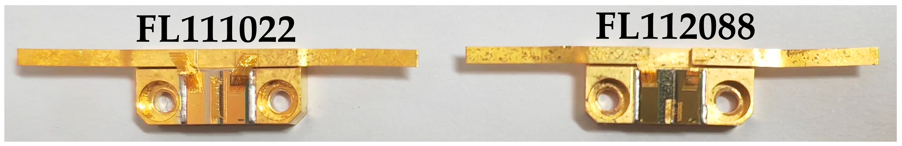
| T3ster | FL111022 | 0.386 | 0.381 | 0.525 | 0.36 | 0.761 | 0.511 | 2.93 |
| FL112088 | 0.331 | 0.33 | 0.42 | 0.35 | 0.689 | 0.4 | 2.52 | |
| Thermal Resistance (K/W) | ||||||||
|---|---|---|---|---|---|---|---|---|
| Chip | R1 | Solder | R2 | Submount | Heat Sink | Rthjc | ||
| T3ster | FL111022 | 0.386 | 0.381 | 0.525 | 0.36 | 0.761 | 0.511 | 2.93 |
| FL112088 | 0.331 | 0.33 | 0.42 | 0.35 | 0.689 | 0.4 | 2.52 | |
| Simulation | 80% | 0.41 | 0.468 | 0.42 | 0.547 | 0.814 | 0.571 | 3.23 |
| 85% | 0.368 | 0.405 | 0.50 | 0.494 | 0.771 | 0.45 | 2.98 | |
| 90% | 0.36 | 0.345 | 0.59 | 0.417 | 0.75 | 0.44 | 2.88 | |
Disclaimer/Publisher’s Note: The statements, opinions and data contained in all publications are solely those of the individual author(s) and contributor(s) and not of MDPI and/or the editor(s). MDPI and/or the editor(s) disclaim responsibility for any injury to people or property resulting from any ideas, methods, instructions or products referred to in the content. |
© 2024 by the authors. Licensee MDPI, Basel, Switzerland. This article is an open access article distributed under the terms and conditions of the Creative Commons Attribution (CC BY) license (https://creativecommons.org/licenses/by/4.0/).
Share and Cite
Deng, L.; Li, T.; Wang, Z.; Zhang, P.; Wu, S.; Liu, J.; Zhang, J.; Chen, L.; Zhang, J.; Huang, W.; et al. Interface Contact Thermal Resistance of Die Attach in High-Power Laser Diode Packages. Electronics 2024, 13, 203. https://doi.org/10.3390/electronics13010203
Deng L, Li T, Wang Z, Zhang P, Wu S, Liu J, Zhang J, Chen L, Zhang J, Huang W, et al. Interface Contact Thermal Resistance of Die Attach in High-Power Laser Diode Packages. Electronics. 2024; 13(1):203. https://doi.org/10.3390/electronics13010203
Chicago/Turabian StyleDeng, Liting, Te Li, Zhenfu Wang, Pu Zhang, Shunhua Wu, Jiachen Liu, Junyue Zhang, Lang Chen, Jiachen Zhang, Weizhou Huang, and et al. 2024. "Interface Contact Thermal Resistance of Die Attach in High-Power Laser Diode Packages" Electronics 13, no. 1: 203. https://doi.org/10.3390/electronics13010203
APA StyleDeng, L., Li, T., Wang, Z., Zhang, P., Wu, S., Liu, J., Zhang, J., Chen, L., Zhang, J., Huang, W., & Zhang, R. (2024). Interface Contact Thermal Resistance of Die Attach in High-Power Laser Diode Packages. Electronics, 13(1), 203. https://doi.org/10.3390/electronics13010203