Article

A Field Programmable Gate Array Placement Methodology for Netlist-Level Circuits with GPU Acceleration

Faculty of Information Technology, Beijing University of Technology, Beijing 100025, China
*
Author to whom correspondence should be addressed.
Electronics 2024, 13(1), 37; https://doi.org/10.3390/electronics13010037
Submission received: 23 November 2023 / Revised: 19 December 2023 / Accepted: 19 December 2023 / Published: 20 December 2023

Abstract

:
Field Programmable Gate Arrays (FPGAs), renowned for their reconfigurable nature, offer unmatched flexibility and cost-effectiveness in engineering experimentation. They stand as the quintessential platform for hardware acceleration and prototype validation. With the increasing ubiquity of FPGA chips and the escalating scale of system designs, the significance of their accompanying Electronic Design Automation (EDA) tools has never been more pronounced. The placement process, serving as the linchpin in FPGA EDA, directly influences FPGA development and operational efficiency. This paper introduces an FPGA placement methodology hinging on the Verilog-to-Routing (VTR) framework. We introduce a novel packing approach grounded in the weighted Edmonds’ Blossom algorithm, ensuring that the CLB generation strategy aligns more closely with load-balanced distribution. Furthermore, we enhanced the electric field-driven resolver placement process for CLB locations and leverage GPU-accelerated design. Experimental results demonstrate substantial improvements over the traditional VTR algorithm, with an average optimization of 28.42% in the packing process runtime, an average acceleration ratio of 2.85 times in the placement phase, and a 39.97% reduction in total packing and placement runtime consumption.

1. Introduction

In recent years, the rapid growth of emerging applications, including the Internet of Things, intelligent computing, and medical electronics, has driven increased market demand for application-specific integrated circuits (ASICs) [1,2,3]. Field Programmable Gate Arrays (FPGAs), known for their reconfigurable nature, offer flexible configuration and cost-effective engineering experimentation. They stand as an ideal development platform for hardware acceleration applications and prototype validation [4,5]. The numerous advantages mentioned above have led to their widespread adoption. The design of FPGAs heavily relies on computer-aided tools (EDA). Within the entire FPGA EDA process, placement represents a pivotal and computationally intensive phase. This step determines the physical placement of various instance units in the design, directly impacting FPGA development and utilization efficiency.
FPGA placement is an NP (nondeterministic polynomial time)-complete combinatorial optimization problem. Early research in FPGA placement in both industry and academia often relied on heuristic algorithms based on simulated annealing [6,7], with a notable example being the Versatile Place and Route (VPR) tool [6,8]. These approaches generated initial solutions in a random manner and perturbed the current solution through global or local exchanges, substitutions, movements, duplications, and other operations to generate new solutions, while these methods can yield relatively desirable placement results, they are associated with longer execution times when dealing with large-scale circuit placement problems [9]. In the subsequent development, both industry and academia transitioned towards minimum-cut algorithms for placement research, with a prominent example being PPFF [10]. These methods employ a recursive netlist partitioning approach, subject to specific constraints, iteratively breaking down the larger placement problem into smaller sub-placement problems. This step-wise process reduces the computational complexity of circuit design but may introduce delays in critical paths. By incorporating graph algorithms and hypergraph partitioning concepts [11,12], minimum-cut algorithms can handle designs comprising thousands of gate units. However, as the gate counts of FPGAs have grown to several million, analytical methods have consistently outperformed the minimum-cut techniques in terms of runtime efficiency and the quality of physical designs. In contrast to the methods mentioned above, analytical techniques describe the placement problem as a more intricate optimization challenge and leverage a diverse set of gradient descent methods for solving it. Analytical methods can be further categorized into quadratic methods [13,14] and non-linear methods [15,16,17]. Quadratic solving entails objective functions composed of quadratic polynomials. Optimal placement results are obtained by solving equations where the first-order derivatives equal zero. Non-linear methods, conversely, use objective functions based on higher-order non-linear equations. Prominent examples of analytical methods include QPF [18], CAPRI [19], StarPlace [20], UTplaceF [14], elfPlace [16], and commercial FPGA placement solvers. Presently, commercial FPGA placement solutions predominantly rely on analytical methods and are recognized for their superior overall performance. In recent years, within the realm of large-scale digital integrated circuit placement research, placement tools based on machine learning methods have begun to emerge [21,22]. These include Google’s EDA achievements based on reinforcement learning [23], the RLPlace placement tool based on reinforcement learning [24], and the DREAMPlace and DREAMPlaceFPGA frameworks with GPU acceleration [25,26]. However, at this stage, addressing the entire process from the circuit netlist to placement remains a challenging endeavor, and the exploration of FPGA placement using artificial intelligence methods is still in its nascent stages [21,27].
This paper presents a novel framework-integrated placement methodology for commercial FPGA processor chip platforms. Firstly, the proposed placement method covered all instance types, and the CLB generation process was constructed using a weighted Edmonds’ Blossom algorithm. Secondly, GPU-based global placement was achieved for industrial-grade netlist circuits, and the entire packing and placement process was completed. Finally, placement experiments were conducted on general netlist circuits, validating the engineering application value of the proposed EDA methodology. Experimental results reveal an average 28.42% optimization in the packing process time, an average acceleration ratio of 2.85 times in the placement phase, and a 39.97% reduction in total packing and placement time compared with traditional VTR.
The rest of this paper is organized as follows. Section 2 introduces the preliminaries of this work. Section 3 presents details of our methodology and algorithm details. Section 4 demonstrates the experimental results. Finally, Section 5 concludes the paper.

2. Related Work

FPGAs are programmable logic chips with a dynamically configurable logic circuit structure that offers increased flexibility and customizability for diverse applications. Despite being manufactured by different vendors, FPGA chips share a similar architecture, differing only in minor local hardware configurations. Figure 1 provides a consolidated overview of the FPGA placement and routing architecture, including the configurable logic block (CLB), digital signal processor (DSP), block random access memory (BRAM), buffer (BUF), and I/O (IO) components. The right side of the figure also depicts the internal structure of the CLB, which consists of several basic logic elements (BLEs), where BLEs are composed of look-up tables (LUTs) and flip-flops (FFs).
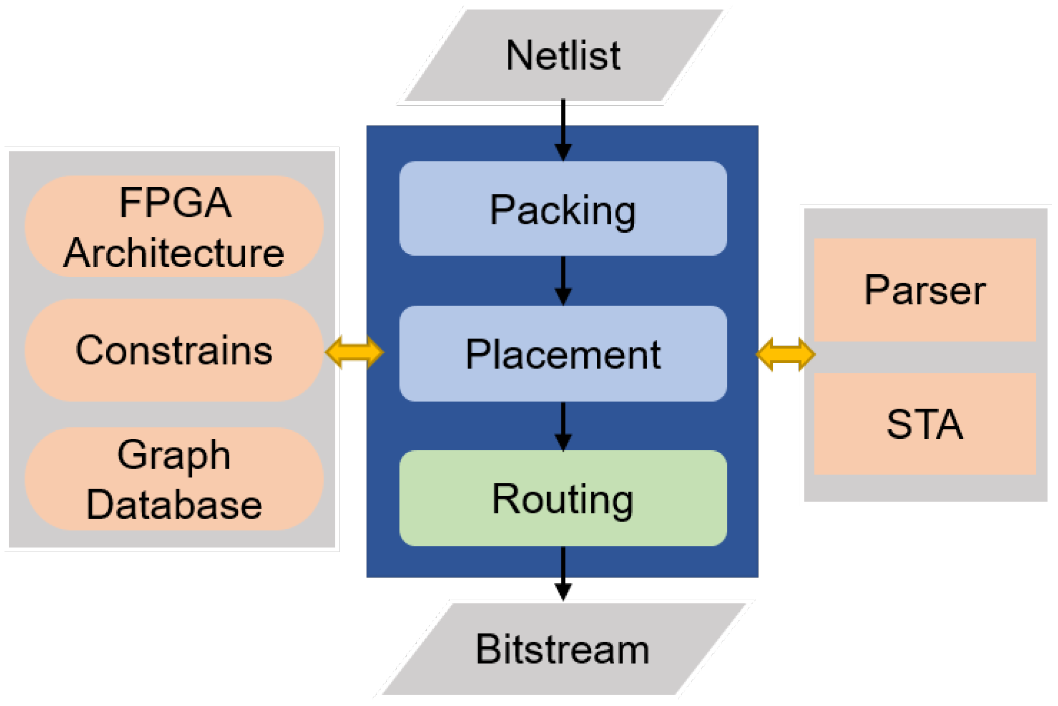
VTR (Verilog to Routing) encompasses a suite of computer-aided design (CAD) tools adaptable to diverse FPGA architectures. Figure 2 outlines the tool process from netlist-level circuits to bitstream generation. Given that the quality of wiring results is predominantly influenced by the placement positions of all instances, the placement phase becomes a pivotal process impacting the entire FPGA EDA tool. Previous research efforts have typically addressed specific issues within the placement process for optimization. It receives the netlist file produced by the synthesis tool, carrying out packing, placement, and performance analysis operations. Eventually, it maps the bitstream file onto the FPGA. The placement process depends on the strategy outcomes of the packing phase. The FPGA packing phase needs to address the allocation of resources to be placed, including the usage of CLB resources and the allocation of resources within the CLB. Subsequently, a predefined number of BLEs are placed within a specific CLB, adhering to predetermined value constraints and optimization conditions. The internal configuration of the CLB remains generally unchanged throughout this process. In the VTR flow, the packaging process logically assigns the circuit netlist to the available resource blocks of the FPGA device, and the resulting information is saved to a .net file. This .net file comprehensively describes the CLB and its associated logic, incorporating details like interconnections, inputs, outputs, and clock signals. Upon completing the packing phase, a placement operation is executed on the circuit. The placement process allocates the resource blocks generated during packing to valid grid locations, optimizing paths and timings. This results in the output of a .place format description file, which details the physical location of all CLB instances. Despite the widely employed simulated annealing algorithm in the placement phase of VTR as a heuristic method, its essence lies in the iterative placement optimization of macrocell modules, resulting in a low granularity of the placement solution. Furthermore, the random placement algorithm for initialized placement struggles to guarantee the placement quality for large-scale circuits, with challenging control over the algorithm’s convergence time. Confronting the characteristics and limitations of the VTR framework, this study embarked on the optimization of the packaged placement algorithm and methodology.

3. Approach

3.1. Proposed Methodology

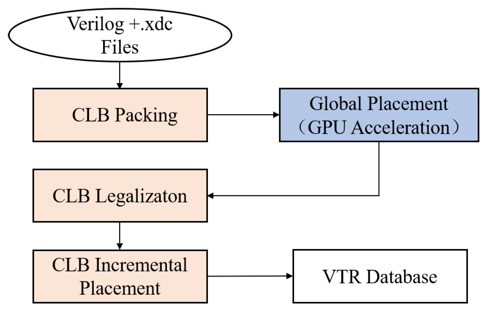
The proposed methodology is illustrated in Figure 3. Specifically, a dedicated parser device is crafted for handling input data in eblif format netlists. Leveraging the VTR netlist read function, this parser extracts essential graph information from the netlist, subsequently integrating it into the optimized DREAMPlaceFPGA framework based on the bookshelf format data. To achieve compatibility with the standard netlist data format, we introduced example additions and modified data interfaces during parsing. The overall workflow involves executing a global placement task using GPU acceleration and seamlessly importing the results into the VTR database. A pivotal aspect of our approach is the introduction of a CLB packing process, grounded in Edmond’s matching algorithm. This process was followed by the development of a CLB legalization process, informed by the outcomes of the packing strategy and global placement data. The results obtained from this comprehensive process serve as the initial state for our parsing method. Building upon this foundation, we employed a sophisticated parsing technique that not only reuses the placement results but also iteratively enhances them to yield refined CLB placement results. These results were then fed into the VTR router, completing the entire process. The proposed methodology integrates seamlessly into the design flow, optimizing the placement of CLBs within the FPGA architecture for enhanced performance and efficiency.

3.2. Parser Design

A key element of the methodology integration process is the parser, and different database types are used between the VTR and GPU acceleration frameworks. Thus, the custom database was designed to bridge the following gaps. GPU acceleration makes use of the bookshelf file interface format, which consists of the following files: . l i b for instance unit properties (pin definitions and directions), . n o d e for units to be placed and their types, . n e t for logical wire and unit graph relationships, . s c l for logical resource distribution in the FPGA chip, and . p l for IO instance position information. The third-party parsing libraries Flex and Bison are used by the GPU acceleration framework to automatically generate grammar programs. The sections on declarations, rules, and C code comprise the core programs. The Flex and Bison libraries’ source code was changed to adapt the lexicon rules for the synthesized netlist text [28]. For example, there is an instance called $techmap1163296$abc$1140382$lut$aiger1140381$99963 in the circuit netlist file. The B o o k s h e l f S c a n n e r . l l file’s rule definition for STRING must be changed to [$A-Za-z][∖∖∖ ][A-Za-z0-9_∖ ∕ ∖ [∖]∖-∖$∖.∖:]* in order to parse it as bookshelf data.

3.3. CLB Packing Design

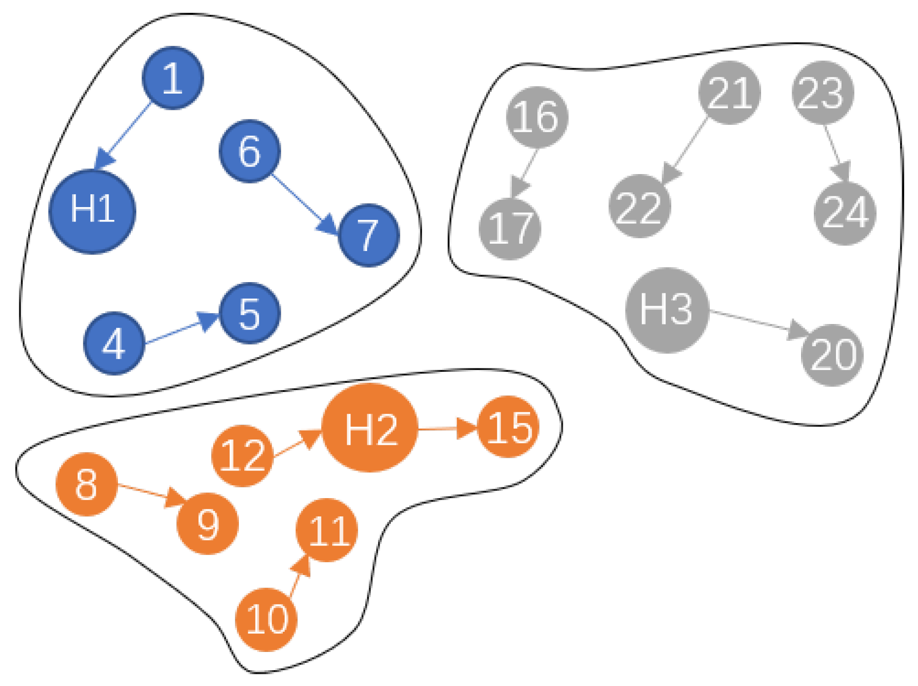
The VTR tool offers a comprehensive packing function based on a greedy algorithm and seed strategy, featuring intricate constraints to address considerations, making it well-suited for small-scale engineering scenarios. However, the current VTR packing and placement exhibit relative independence, particularly with the packing phase being time-consuming. This presents a significant opportunity for runtime optimization. To address this, our study focuses on refining the CLB merger generation strategy. We propose a CLB generation strategy based on Edmond matching, aiming to enhance the efficiency of the packing phase. The key adjustment involves conducting CLB clustering generation in strict accordance with logical relationships. By increasing the number of CLB clustering instances, we aim to not only improve packing time but also significantly increase the volume of placement tasks. The motivation behind this approach is to exploit GPU acceleration technology more effectively. This involves leveraging the parallel processing capabilities of GPUs to handle a larger number of placement tasks concurrently. Our strategy is illustrated in detail in Figure 4, Figure 5 and Figure 6. The LUT and FF graphs are established using information from the static timing analysis report (Figure 4 illustrates the initial state relationship of the node graph, encompassing nodes 1–24, utilizing a directed graph to represent time paths between cells with node weights calibrated by static timing results). Subsequently, the hypergraph of the register group is derived through the HCS (Highly Connected Subgraph) algorithm [29], as depicted in Figure 5, forming clustering points H1(2,3), H2(13,14), and H3(18,19). This newly formed hypergraph enables the calculation of the evaluation function and constraint function. The evaluation function, in this study, is expressed as the sum of weights, while the constraint function considers the number of cells accommodated within the CLB and the total number of CLBs. Employing the Edmond maximum weight matching algorithm [30], clustering results were obtained to ensure relative balance within each CLB block. Figure 6 illustrates the formation of division regions, with each region capable of independently performing CLB generation.
We constructed an undirected weighted graph Node = (V; E). The pseudo-code of the weighted Edmonds’ Blossom algorithm for CLB packing is summarized in Algorithm 1. Each connected subgraph is constructed by the HCS merging process. Nodes and edges are added into the subgraph in a breadth-first search manner. When the subgraph stops growing, the max-weighted matching is run on the constructed subgraph, and mergings corresponding to matched edges are committed to the graph. The loop of constructing subgraphs, solving max-weighted matching, and committing matched mergings is iterative and stops when no more merging can be performed.
Algorithm 1 Weighted Edmonds’ Blossom Algorithm for CLB Packing
Require: CLB division regions are planned.
Ensure: LUTs and FFs relation graph built.
1: while ture do
2:    Initialize data structure.
3:     n u m _ m a t c h i n g 0
4:    for  v V  do
5:        HCS merging process.
6:        Edmonds’ blossom matching process.
7:    end for
8:    if  n u m _ m a t c h i n g meet constraints then
9:        return
10:    end if
11: end while
In summary, our study introduces a novel CLB generation strategy based on Edmond matching, emphasizing the logical relationships between CLBs. This strategic adjustment is anticipated to optimize the packing phase of VTR, leading to reduced runtime and improved efficiency. The proposed approach holds potential for unlocking the benefits of GPU acceleration technology, enabling more scalable and efficient placement in VTR for a wider range of engineering scenarios.

3.4. Improvements to the GPU Acceleration Framework

The DREAMPlaceFPGA framework is currently in its early stages, offering a significant advantage by presenting a generalized solution for GPU-based EDA problems, albeit primarily focused on global placement challenges [26]. The framework encompasses various operators within its op layer, including adjust_node_area, clustering_compatibility, dct, demandMap, density_map, pin_pos, pin_utilization, place_io, precondWL, rmst_wl, rudy, utility, and weighted_average_wirelength. To enhance its practical applicability, particularly for netlist circuits adapted to general-purpose use (refer to the parser section for specifics), additional considerations should be made to meet the resource requirements of the target FPGA chip. Specific instances on the DREAMPlaceFPGA side, such as the adder unit (CARRY) and data selector (MUX) for the developed FPGA chip, need supplementation in line with the resource demands of the adapted FPGA. The original framework leads to unclear goals of optimization because it considers too trivial instance placement. To optimize DREAMPlaceFPGA placement outcomes, a direct CLB placement method based on IO port anchors was designed. Given DREAMPlaceFPGA’s flexibility regarding the number of instances for placement processing, a global placement approach is adopted for all instances, while other tasks are executed within the VTR framework. In the current phase, the DREAMPlaceFPGA framework functions as a subprocess in the methodology, playing a role akin to that of a chip coprocessor.
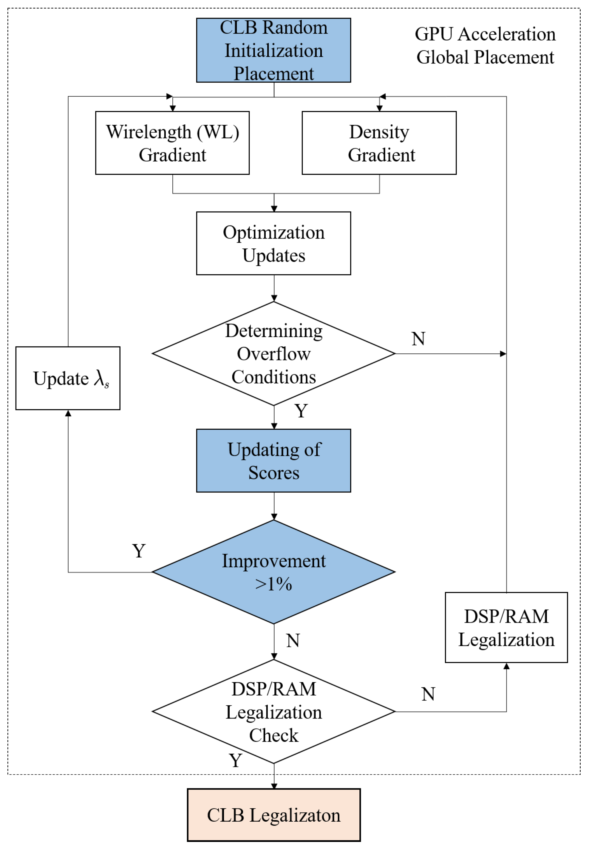
In our project, the global placement algorithm of the GPU acceleration framework is extracted as a sub-process within the fusion framework. The global placement method, as illustrated in Figure 7, initiates with a CLB initialized placement phase, distributing cells within the placement area’s center and arranging them randomly. Subsequently, the core computation of global placement is seamlessly integrated into the deep learning framework. Equation (1) characterizes the classical optimization objective function for global placement, where D ( x , y ) denotes the density statistics of instance objects at the position ( x , y ) and W e ( x , y ) represents the HPWL statistics of net e in the set of nets E. The unit density control factor is indicated by λ . A more sophisticated nonlinear global placement algorithm is presented in elfPlace [16]. The Weighted Average (WA) model can be introduced based on the definition of electrostatic placement. Equation (2) expresses the HPWL (Half-Perimeter Wirelength) statistics of net e, Equation (3) expresses the W A statistics in the x direction, and Equation (4) describes the overall WA wirelength statistics. The solution objective of the nonlinear placement problem is corrected based on the Augmented Lagrange Method (ALM) [31] by comparing the potential density of the electrostatic system and the WA wirelength model, as shown in Equation (5). Here, the device set s S = { C L B , I O , D S P , R A M } , and λ s and ϕ s indicate the density control factor and the expression for electrical energy, respectively. The expression for the electrical energy calculation can be based on the Poisson distribution for column writing, where c s stands for the quadratic control factor. The α and β then denote the tuning factors to obtain more optimized results. The discrete trigonometric function transformation method is used to solve the electrostatic Poisson equation. The neural network training problem in Equation (1) is converted into a GPU-accelerated framework for FPGA placement. In order to create deep learning solution mapping, coordinate data y are used as the label quantity when coordinate data x are input into the neural network. Different device units can be regarded as distinct objects for placement calculations in the FPGA placement process. The overall score of the current distribution is derived from a combination of HPWL and timing estimation results. The iterative process is controlled by evaluating the incremental percentage, as illustrated in Figure 7. Upon successful DSP/RAM legalization verification, the CLB undergoes adjustment for legalized placement and subsequent incremental optimization.
m i n x , y f ( x , y ) = lim ( e E W e ( x , y ) + λ D ( x , y ) )
W ( x , y ) = e E ( m a x i , j E x i x j + m a x i , j E y i y j )
W ˜ e x = i e x i e x p ( x i γ ) i e e x p ( x i γ ) i e x i e x p ( x i γ ) i e e x p ( x i γ )
W ˜ ( x , y ) = e E ( W ˜ e x + W ˜ e y )
m i n x , y f ( x , y ) = α · W ˜ ( x , y ) + β · s S λ s ( ϕ s ( x , y ) + c s 2 ϕ s ( x , y ) 2 )

3.5. Incremental Optimization

CLB legalization is required based on the GPU-accelerated global placement results and the CLB clustering generation strategy. The goal is to give each CLB instance a reasonable location that is closest to the results of the GPU-accelerated global placement. Algorithm 2 presents the comprehensive algorithm design for the placement of CLB legalization. The main concept of discrete search in the surrounding area is incorporated into the overall algorithm. The discretized vector data type b i n _ s o u r c e , which completely encapsulates the FPGA’s physical resource information, is used to represent the layoutable resources in the GPU-accelerated global placement results. The legalized locations of CLB instances, indicated by the variable c l b _ l e g a l _ l o c a t i o n , are the output data. In Step 1, instance unit weights are sorted by criticality based on CLB cluster/class score statistics and physical constraints; the array of CLBs pending legalization is denoted by s o r t _ c l b . The storage identifier in each CLB database is represented in Step 2 by b l k _ i d . The horizontal and vertical coordinates are calculated using the nearest neighbor algorithm, and the associated solving function is designated as n e a r e s t _ l o c a t i o n ( b l k _ i d ). As explained in Algorithm Step 3, the computation results are kept in the c l b _ l o c a t i o n structure database. Step 4 verifies the legality of b i n _ s o u r c e and c l b _ l o c a t i o n based on placement rules, in accordance with the patterns of physical resource allocation in domestic FPGAs. This is achieved by verifying whether the location is occupied by other instances, whether resource conflicts exist, and whether it corresponds with the physical characteristics of the corresponding instances. If the constraints are satisfied, the legal placement information can be output. Otherwise, incremental adjustments to the location coordinates in the neighboring region are made to achieve legal placement for CLBs.
Algorithm 2 CLB Legalization
Input:  g l o b a l _ l o c a t i o n , FPGA source, b i n _ s o u r c e .
Output: CLB Legalization Location: c l b _ l e g a l _ l o c a t i o n .
1: Instance unit weights sorted to form initial to-be-legalized array s o r t _ c l b .
2: for  ( a u t o b l k _ i d : s o r t _ C L B )  do
3:     c l b _ l o c a t i o n   n e a r e s t _ l o c a t i o n ( b l k _ i d )
4:    if  b i n _ s o u r c e , c l b _ l a c a t i o n , Legalization rule determination then
5:          p u s h _ b a c k ( c l b _ l o c a t i o n )
6:    else
7:          Incremental adjustment of the calculated value of the coordinates.
8:    end if
9: end for
Based on the VTR API, an incremental placement is achieved by reducing the process iteration to optimize the placement quality. The specific algorithm design is illustrated in Algorithm 3, where the input is the legal CLB placement, c l b _ l e g a l _ l o c a t i o n , and the output is the optimized CLB placement, denoted as c l b _ o p t i m i z e d _ l o c a t i o n . The VTR parsing API function A P _ r u n ( ) is utilized for calculations, considering constraints. The iteration count N is adjusted to control the runtime overhead of detailed placement, where HPWL needs to adhere to local optimal constraints, and timing results should meet design requirements.
Algorithm 3 CLB Incremental Placement
Input: CLB Optimized Location.
Output: CLB Legalization Location: c l b _ l e g a l _ l o c a t i o n .
     while Number of iterations N && HPWL local optimal solution && Timing result satisfied do
2:    AP_run( )
        Collect statistical HPWL and timing results.
4:    N- -
     end while

4. Experimental Results

All experiments presented in this paper were conducted using the FPGA general-purpose interface development board. The FPGA chip model employed is part of the Zynq UltraScale+ series developed by Xilinx Corporation [32]. Figure 8 illustrates a schematic diagram of the development board along with the corresponding FPGA chip sample. The XCZU7EV-FFVC1156AAZ is fabricated using the 16 nm FinFET process node and boasts specifications including 504K logic cells, 230.4K LUTs, 1728 DSPs, and 11Mb BRAM. It adopts a stacked modularized placement, reinforcing the hierarchical characteristics of the overall architectural design.
The benchmark circuit test set was selected from open-source test benchmarks in VTR and OpenCores [33,34]. The baseline program for comparative experiments utilizes the VTR source code. Our methodology, which combines the proposed algorithm and GPU acceleration with the VTR framework, focuses on comparing the time required for the packing and placement processes. The GPU acceleration methodology extends the PyTorch and DREAMPlace frameworks [25,26,35]. The included operator (op) layers consist of adjust_node_area, clustering_compatibility, dct, demand_map, density_map, pin_pos, pin_utilization, place_io, precondWL, rmst_wl, rudy, utility, and weighted_average_wirelength. The algorithm prototypes are fitted with a flexible combination of op and GPU adaptation. The hardware platform for the entire experiment consists of an Intel Core i5-10500 CPU, 36GB of RAM, and an NVIDIA A10 GPU running Linux Ubuntu 18.04.
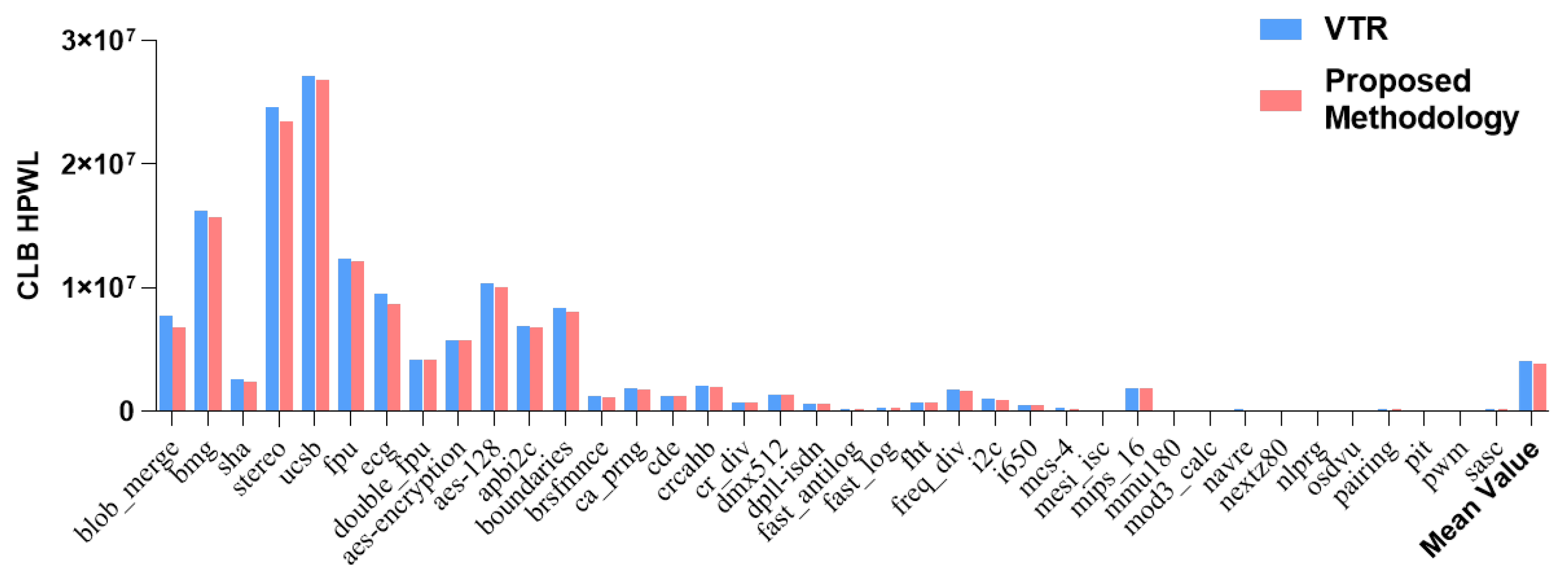
Figure 9 and Figure 10 illustrate the runtime statistics for selected test cases under various platform conditions using GPU acceleration, comparing the time between CPU- and GPU-accelerated implementations. On average, the packing process time is reduced by 28.42% due to the decreased computational complexity of the optimization algorithm. The experimental results demonstrate that the utilization of GPUs accelerates the placement program. The runtime for the CPU group ranges from 3.32 s to 171.78 s, while the GPU group’s runtime varies from 1.32 s to 61.50 s. The speedup ratio ranges from 1.10 times to 5.55 times, with an average of 2.85 times. Regarding the initial CLB half perimeter wire length (HPWL), the original VTR process shows a minimum HPWL of 22,139 and a maximum of 27,125,48. In our proposed methodology, the minimum HPWL is 21,304, and the maximum is 26,856,911. As the number of HPWL is associated with the scale and characteristics of the benchmark circuits, Figure 11 visually depicts the percentage reduction in the initial HPWL compared to the original VTR process. The minimum reduction percentage is 0.19%, and the maximum is 11.50%, with an average HPWL reduction of 3.73%.
Table 1 offers a comprehensive statistical comparison between the original VTR and our proposed methodology concerning the packing time, placement time, CLB HPWL, and the total runtime of the packing and placement process. The experimental results demonstrate that, in comparison to the traditional algorithms used by VTR, the total packing and placement time is optimized by an average of 39.97%. The adjustment of the CLB merge generation strategy, conducting CLB clustering based on logical relationships, and appropriately increasing the number of generated CLBs effectively reduce the packing time overhead. Furthermore, GPU acceleration can significantly enhance the efficiency of distributed computing in the placement phase. Moreover, leveraging the weighted Edmonds’ Blossom algorithm, we attain an improved combination of CLB logic. This not only results in a higher HPWL gain but also optimizes timing outcomes, leading to an average maximum frequency increase of 5.08 MHz. The detailed data can be referenced in Freq. (frequency) columns of Table 1. Notably, all experiments were conducted using the open-source synthesizer Yosys tool, with a synthesis phase maximum frequency set to 300 MHz. In addition, the CLB resource utilization of the hardware remains at the same level, with an average percentage reduction of 2.09% compared to the VTR, as depicted in the CLB Util. (utilization) columns of Table 1.
To underscore the versatility of the GPU acceleration framework in handling very large-scale netlisting circuits, we conducted a methodology validation using a million-gate scale System-on-Chip (SoC) netlisting, specifically BJUT-RISC [36]. Table 2 details the FPGA resource overhead statistics, with the utilization rate of LUTs exceeding 90%. Notably, the benchmarked BJUT-RISC faced challenges completing placement experiments on VTR due to memory constraints (limited to 36GB RAM on the experimental machine). In contrast, our proposed methodology not only accomplished the entire placement process but also capitalized on GPU acceleration, demonstrating its effectiveness in overcoming memory limitations. Figure 12 illustrates the runtime overhead statistics for benchmarking BJUT-RISC. The GPU-accelerated step consumes a mere 0.23 h, constituting only 8% of the overall process. This highlights the optimization impact achieved through GPU acceleration, with the detailed placement time of CLBs standing at a commendable 0.97 h.
The outcomes of the global placement, when processed through the devised legalization algorithm, proficiently detect suboptimal solutions during the placement stage. Subsequent local optimization through the detailed placement algorithm results in a decreased number of iterations, thereby optimizing the placement process time. Hence, the proposed FPGA placement methodology is well-suited for the Xilinx FPGA processor chip XCZU7EV-FFVC1156AAZ, efficiently accomplishing the packing and placement tasks.

5. Conclusions

In this paper, we present an enhanced EDA methodology for FPGA packing and placement processes by leveraging the VTR and GPU acceleration frameworks. By optimizing algorithms and fine-tuning process parameters, we enhance the efficiency of traditional VTR methodology’s packing and placement algorithms. The practicality of the GPU acceleration framework is extended, and a novel approach to FPGA placement is introduced by integrating different frameworks. Experimental results reveal an average 28.42% optimization in the packing process time, an average acceleration ratio of 2.85 times in the placement phase, and a 39.97% reduction in total packing and placement time compared to traditional algorithms, demonstrating engineering feasibility. Furthermore, we showcase the applicability of the proposed methodology to ultra-large-scale industrial-grade netlist circuits. In future work, we plan to explore multi-objective placement optimization problems and streamline the CUDA programming framework to improve the quality of packing and placement results, along with enhancing the usability and practicality of the programming interface.

Author Contributions

Methodology, M.L.; software, Y.W.; original draft preparation, Y.W. and M.L.; review and editing, M.L.; analysis and validation, S.L. All authors have read and agreed to the published version of the manuscript.

Funding

This work was supported in part by the Beijing Natural Science Foundation (No. 4234089).

Data Availability Statement

Data are contained within the article.

Conflicts of Interest

The authors declare no conflict of interest.

References

  1. Przybył, A. FPGA-Based Optimization of Industrial Numerical Machine Tool Servo Drives. Electronics 2023, 12, 3585. [Google Scholar] [CrossRef]
  2. Li, D.; Feng, X.; Shen, C.; Chen, Q.; Yang, L.; Qiu, S.; Jin, X.; Liu, M. Vector-Based Dedicated Processor Architecture for Efficient Tracking in VSLAM Systems. IEEE Embed. Syst. Lett. 2023, 15, 182–185. [Google Scholar] [CrossRef]
  3. Zhang, Z.; Liu, M.; Liu, Z.; Du, X.; Xie, S.; Ma, H.; Ding, G.; Ren, W.; Zhou, F.; Sun, W.; et al. Progress in a novel architecture for high performance processing. Jpn. J. Appl. Phys. 2018, 57, 04FA03. [Google Scholar] [CrossRef]
  4. Hikawa, H. Place-and-Route Analysis of FPGA Implementation of Nested Hardware Self-Organizing Map Architecture. Electronics 2023, 12, 4523. [Google Scholar] [CrossRef]
  5. Li, R.; Wu, J.; Liu, M.; Chen, Z.; Zhou, S.; Feng, S. HcveAcc: A high-performance and energy-efficient accelerator for tracking task in VSLAM system. In Proceedings of the 2020 Design, Automation & Test in Europe Conference & Exhibition (DATE), Grenoble, France, 9–13 March 2020; pp. 198–203. [Google Scholar]
  6. Betz, V.; Rose, J. VPR: A new packing, placement and routing tool for FPGA research. In International Workshop on Field Programmable Logic and Applications, Proceedings of the 7th International Workshop, FPL ’97, London, UK, 1–3 September 1997; Springer: Cham, Switzerland, 1997; pp. 213–222. [Google Scholar]
  7. Chen, G.; Cong, J. Simultaneous placement with clustering and duplication. In Proceedings of the 41st Annual Design Automation Conference, San Diego, CA, USA, 7–11 June 2004; pp. 740–772. [Google Scholar]
  8. Betz, V.; Rose, J. Automatic generation of FPGA routing architectures from high-level descriptions. In Proceedings of the 2000 ACM/SIGDA Eighth International Symposium on Field Programmable Gate Arrays, Monterey, CA, USA, 10–11 February 2000; pp. 175–184. [Google Scholar]
  9. Yu, L.; Guo, B. Timing-Driven Simulated Annealing for FPGA Placement in Neural Network Realization. Electronics 2023, 12, 3562. [Google Scholar] [CrossRef]
  10. Maidee, P.; Ababei, C.; Bazargan, K. Timing-driven partitioning-based placement for island style FPGAs. IEEE Trans. Comput.-Aided Des. Integr. Circuits Syst. 2005, 24, 395–406. [Google Scholar] [CrossRef]
  11. Karypis, G.; Kumar, V. Multilevel k-way hypergraph partitioning. In Proceedings of the 36th Annual ACM/IEEE Design Automation Conference, New Orleans, LA, USA, 21–25 June 1999; pp. 343–348. [Google Scholar]
  12. Fiduccia, C.M.; Mattheyses, R.M. A Linear-Time Heuristic for Improving Network Partitions. Papers on Twenty-Five Years of Electronic Design Automation. 1988, pp. 241–247. Available online: https://dl.acm.org/doi/pdf/10.1145/62882.62910 (accessed on 18 December 2023).
  13. Gort, M.; Anderson, J.H. Analytical placement for heterogeneous FPGAs. In Proceedings of the 22nd International Conference on Field Programmable Logic and Applications (FPL), Oslo, Norway, 29–31 August 2012; pp. 143–150. [Google Scholar]
  14. Li, W.; Dhar, S.; Pan, D.Z. UTPlaceF: A routability-driven FPGA placer with physical and congestion aware packing. IEEE Trans. Comput.-Aided Des. Integr. Circuits Syst. 2017, 37, 869–882. [Google Scholar] [CrossRef]
  15. Chen, Y.C.; Chen, S.Y.; Chang, Y.W. Efficient and effective packing and analytical placement for large-scale heterogeneous FPGAs. In Proceedings of the 2014 IEEE/ACM International Conference on Computer-Aided Design (ICCAD), San Jose, CA, USA, 2–6 November 2014; pp. 647–654. [Google Scholar]
  16. Meng, Y.; Li, W.; Lin, Y.; Pan, D.Z. elfplace: Electrostatics-based placement for large-scale heterogeneous fpgas. IEEE Trans. Comput.-Aided Des. Integr. Circuits Syst. 2021, 41, 155–168. [Google Scholar] [CrossRef]
  17. Zhu, Z.; Mei, Y.; Deng, K.; He, H.; Chen, J.; Yang, J.; Chang, Y.W. High-performance Placement Engine for Modern Large-scale FPGAs With Heterogeneity and Clock Constraints. IEEE Trans. Comput.-Aided Des. Integr. Circuits Syst. 2023. [Google Scholar] [CrossRef]
  18. Xu, Y.; Khalid, M.A. QPF: Efficient quadratic placement for FPGAs. In Proceedings of the International Conference on Field Programmable Logic and Applications, Tampere, Finland, 24–26 August 2005; pp. 555–558. [Google Scholar]
  19. Gopalakrishnan, P.; Li, X.; Pileggi, L. Architecture-aware FPGA placement using metric embedding. In Proceedings of the 43rd Annual Design Automation Conference, San Francisco, CA, USA, 24–28 July 2006; pp. 460–465. [Google Scholar]
  20. Xu, M.; Gréwal, G.; Areibi, S. StarPlace: A new analytic method for FPGA placement. Integration 2011, 44, 192–204. [Google Scholar] [CrossRef]
  21. Taj, I.; Farooq, U. Towards Machine Learning-Based FPGA Backend Flow: Challenges and Opportunities. Electronics 2023, 12, 935. [Google Scholar] [CrossRef]
  22. Baig, I.; Farooq, U. Efficient Detailed Routing for FPGA Back-End Flow Using Reinforcement Learning. Electronics 2022, 11, 2240. [Google Scholar] [CrossRef]
  23. Mirhoseini, A.; Goldie, A.; Yazgan, M.; Jiang, J.W.; Songhori, E.; Wang, S.; Lee, Y.J.; Johnson, E.; Pathak, O.; Nazi, A.; et al. A graph placement methodology for fast chip design. Nature 2021, 594, 207–212. [Google Scholar] [CrossRef] [PubMed]
  24. Mallappa, U.; Pratty, S.; Brown, D. RLPlace: Deep RL guided heuristics for detailed placement optimization. In Proceedings of the 2022 Design, Automation & Test in Europe Conference & Exhibition (DATE), Antwerp, Belgium, 14–23 March 2022; pp. 120–123. [Google Scholar]
  25. Lin, Y.; Dhar, S.; Li, W.; Ren, H.; Khailany, B.; Pan, D.Z. Dreamplace: Deep learning toolkit-enabled gpu acceleration for modern vlsi placement. In Proceedings of the 56th Annual Design Automation Conference, Las Vegas, NV, USA, 2–6 June 2019; pp. 1–6. [Google Scholar]
  26. Rajarathnam, R.S.; Alawieh, M.B.; Jiang, Z.; Iyer, M.; Pan, D.Z. DREAMPlaceFPGA: An open-source analytical placer for large scale heterogeneous FPGAs using deep-learning toolkit. In Proceedings of the 2022 27th Asia and South Pacific Design Automation Conference (ASP-DAC), Taipei, Taiwan, 17–20 January 2022; pp. 300–306. [Google Scholar]
  27. Goswami, P.; Bhatia, D. Congestion Prediction in FPGA Using Regression Based Learning Methods. Electronics 2021, 10, 1995. [Google Scholar] [CrossRef]
  28. Levine, J. Flex & Bison: Text Processing Tools; O’Reilly Media, Inc.: Sebastopol, CA, USA, 2009. [Google Scholar]
  29. Xu, D.; Tian, Y. A comprehensive survey of clustering algorithms. Ann. Data Sci. 2015, 2, 165–193. [Google Scholar] [CrossRef]
  30. Gabow, H.N.; Kaplan, H.; Tarjan, R.E. Unique maximum matching algorithms. In Proceedings of the Thirty-First Annual ACM Symposium on Theory of Computing, Atlanta, GA, USA, 1–4 May 1999; pp. 70–78. [Google Scholar]
  31. Zhu, Z.; Chen, J.; Peng, Z.; Zhu, W.; Chang, Y.W. Generalized augmented lagrangian and its applications to VLSI global placement. In Proceedings of the 55th Annual Design Automation Conference, San Francisco, CA, USA, 24–29 June 2018; pp. 1–6. [Google Scholar]
  32. Churiwala, S.; Hyderabad, I. Designing with Xilinx® FPGAs. In Circuits & Systems; Springer: Berlin/Heidelberg, Germany, 2017. [Google Scholar]
  33. Wolf, C.; Glaser, J.; Kepler, J. Yosys-a free Verilog synthesis suite. In Proceedings of the 21st Austrian Workshop on Microelectronics (Austrochip), Linz, Austria, 10 October 2013; p. 97. [Google Scholar]
  34. Meng, L.; Shuai, L.; Yunfei, W.; Huixin, P.; Chunxue, L.; Liang, W. HDLcs1. 0: A Compiler and Simulator Framework for Hardware Description Language. In Proceedings of the 2023 International Symposium of Electronics Design Automation (ISEDA), Nanjing, China, 8–11 May 2023; pp. 93–96. [Google Scholar]
  35. Paszke, A.; Gross, S.; Massa, F.; Lerer, A.; Bradbury, J.; Chanan, G.; Killeen, T.; Lin, Z.; Gimelshein, N.; Antiga, L.; et al. Pytorch: An imperative style, high-performance deep learning library. In Proceedings of the Advances in Neural Information Processing Systems 32 (NeurIPS 2019), Vancouver, BC, Canada, 8–14 December 2019. [Google Scholar]
  36. Liu, M. A co-design method of customized ISA design space exploration and fixed-point library construction for RISC-V dedicated processor. IEICE Electron. Express 2022, 19, 20220244. [Google Scholar] [CrossRef]
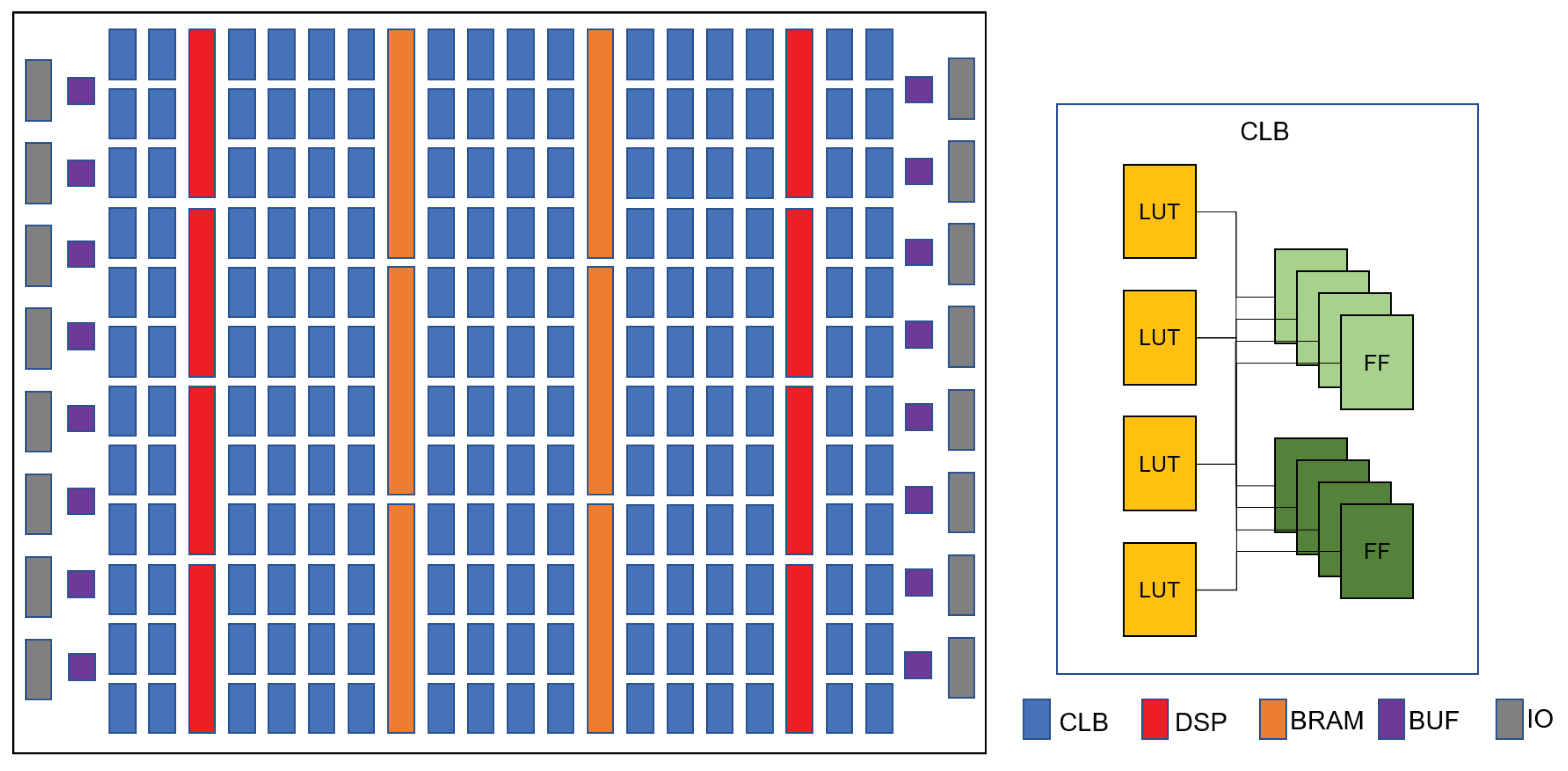
Figure 1. A representative FPGA placement architecture schematic.
Electronics 13 00037 g001
Figure 2. The traditional methodology of FPGA EDA. Among other aspects, the EDA database covers the FPGA architecture, constraint information, and graph database. Plug-in class tools include the parser and static timing analysis (STA) tool.
Electronics 13 00037 g002
Figure 3. The proposed methodology of FPGA packing and placement.
Electronics 13 00037 g003
Figure 4. Several LUT and FF relationship graphs.
Electronics 13 00037 g004
Figure 5. After HCS merging, several LUTs and FFs are hypergraphically interconnected.
Electronics 13 00037 g005
Figure 6. Schematic diagram illustrating the formation of CLB division regions.
Electronics 13 00037 g006
Figure 7. The GPU acceleration framework for CLB global placement based on DREAMPlaceFPGA.
Electronics 13 00037 g007
Figure 8. The schematic diagram of the development board and corresponding XCZU7EV-FFVC1156AAZ chip.
Electronics 13 00037 g008
Figure 9. The comparison of packing time between VTR and the proposed methodology.
Electronics 13 00037 g009
Figure 10. The comparison of CLB HPWL between VTR and the proposed methodology.
Electronics 13 00037 g010
Figure 11. The comparison of placement time between VTR and the proposed methodology.
Electronics 13 00037 g011
Figure 12. Runtime overhead statistics for benchmarking BJUT-RISC.
Electronics 13 00037 g012
Table 1. Comparisons between the VTR flow and our proposed methodology.
Benchmarks 1VTRProposed Methodology
Packing
Time (s)
Placement
Time (s)
Total
Time (s)
CLB
HPWL
Freq.
(MHz)
CLB
Util.
Packing
Time (s)
Placement
Time (s)
Total
Time (s)
CLB
HPWL
Freq.
(MHz)
CLB
Util.
blob_merge35.1916.6551.847706102282.6213.10%23.914.0627.976819560286.4010.35%
bmg94.5569.73164.2816182815271.4328.37%67.1737.67104.8415711471277.7525.48%
sha10.773.6314.402568701286.154.21%6.521.327.842378427297.582.17%
stereo127.1515.81142.9624659527265.8935.82%100.646.07106.7123485264266.7433.24%
ucsb260.3927.50287.8927125480261.8343.16%226.4512.38238.8326856911262.1940.99%
fpu135.5433.20168.7412329764268.9727.53%95.2812.70107.9812088004269.6024.84%
ecg83.6422.50106.149484434273.7826.21%58.6420.4079.048701315275.8923.21%
double_fpu10.548.2118.754123667285.637.12%7.401.899.294115436296.524.97%
aes-encryption24.6416.3240.965773133278.3611.86%17.465.7623.225699046284.699.17%
aes-128148.5430.43178.9710391640269.2727.93%99.238.53107.769991962278.0526.07%
apbi2c63.2866.50129.786927760282.3814.78%45.1215.0560.176725981286.0213.48%
boundaries289.47100.45389.928313312263.4542.32%201.7518.10219.858039954263.7240.83%
brsfmnce16.9114.5031.411187616287.8610.51%11.683.9015.581100830297.128.03%
ca_prng57.8249.78107.601900186283.2113.75%40.2216.9557.171881187286.1910.79%
cde42.9918.4361.421187616280.4311.40%29.957.2937.241096672283.689.28%
crcahb78.1334.54112.672018947271.3918.65%54.0612.6666.721927769273.1017.31%
cr_div11.2632.0843.34747758287.448.34%7.831.839.66681233297.366.01%
dmx51247.5328.8176.341345965279.6212.54%33.027.6740.691238855282.8911.05%
dpll-isdn17.4213.4230.84611802286.879.16%12.142.9315.07565370295.256.63%
fast_antilog6.883.3210.20197356281.923.25%4.791.986.77184318299.751.78%
fast_log31.7720.7052.47276298280.4512.93%22.079.1031.17276256283.9411.64%
fht75.2234.70109.92663115278.9314.87%51.9612.3664.32620420280.5013.32%
freq_div162.33100.11262.441724098267.3928.36%112.9825.90138.881698974268.2527.19%
i2c97.0989.03186.121014175277.3425.32%67.3925.0592.44977281279.1122.33%
i65051.0826.9177.99533776278.5313.83%35.5214.6350.15504092282.0710.93%
mcs-428.7515.6344.38242626283.898.56%20.084.8524.93242039289.917.32%
mesi_isc7.444.2011.6456425285.125.75%5.181.907.0853854297.273.87%
mips_16213.02171.78384.801884581257.2840.43%148.0061.50209.501761781257.9138.15%
mmu18018.9916.3635.3531410283.2610.77%13.165.5718.7329221290.679.40%
mod3_calc43.2118.4361.6459678281.5111.65%30.117.2937.4057425286.889.15%
navre89.0737.37126.44137260278.6714.36%62.0215.2577.27127944282.0312.68%
nextz8012.568.4621.0222139288.457.67%8.732.1510.8821792297.985.22%
nlprg46.3328.9075.2379700280.9612.86%32.287.8040.0876753285.9411.17%
osdvu55.7838.5694.34103609279.1613.43%39.0016.1555.1594854283.8310.75%
pairing107.2643.95151.21165775275.3926.18%75.0020.9095.90154530277.1024.42%
pit19.8413.3633.2031278285.299.07%13.725.5019.2228968293.947.51%
pwm67.5532.3199.86106346277.4614.21%46.8818.4565.3397470281.3812.01%
sasc126.3444.54170.88175471274.2327.17%88.6821.22109.90166121275.6625.13%
Mean Value74.1135.56109.674002404277.9417.56%53.0512.4965.553849456283.0215.47%
1 blob_merge: image processing; bmg: finance calculation; sha: cryptography; stereo: computer vision; ucsb: educational CPU module; fpu: floating point unit; ecg: signal processing; double_fpu: double-precision floating point unit; aes-encryption: cryptography; aes-128: cryptography; apbi2c: bus protocol; boundaries: clock boundaries; brsfmnce: synchronous FIFO; ca_prng: cellular automata; cde: codec module; crcahb: bus protocol; cr_div: cached reciprocal divider; dmx512: communication controller; dpll-isdn: digital phase locked loop; fast_antilog: anti-logarithm calculation; fast_log: logarithm calculation; fht: fast Hartley transform; freq_div: adjustable frequency divider; i2c: bus protocol; i650: data storage module; mcs-4: data processing module; mesi_isc: coherency intersection controller; mips_16: educational CPU module; mmu180: memory management unit; mod3_calc: divider module; navre: multimedia application module; nextz80: combinatorial logic; nlprg: pseudo-random generator; osdvu: UART component; pairing: pairing algorithm module; pit: programmable interval timer; pwm: pulse width modulator; sasc: asynchronous serial controller.
Table 2. FPGA resource overhead statistics for a multi-million gate netlist circuit.
Site TypeAvailableUsedUtilization
LUTs2304002172540.94
FFs4608001655800.36
BRAM1180.73
DSP172913400.78
Disclaimer/Publisher’s Note: The statements, opinions and data contained in all publications are solely those of the individual author(s) and contributor(s) and not of MDPI and/or the editor(s). MDPI and/or the editor(s) disclaim responsibility for any injury to people or property resulting from any ideas, methods, instructions or products referred to in the content.