Article

Current-Prediction-Controlled Quasi-Z-Source Cascaded Multilevel Photovoltaic Inverter

School of Electrical and Electronic Engineering, Harbin University of Science and Technology, Harbin 150080, China
*
Author to whom correspondence should be addressed.
Electronics 2024, 13(10), 1824; https://doi.org/10.3390/electronics13101824
Submission received: 19 March 2024 / Revised: 22 April 2024 / Accepted: 6 May 2024 / Published: 8 May 2024
(This article belongs to the Special Issue Power Electronics in Renewable Systems)

Abstract

:
To address problems that traditional two-stage inverters suffer such as high cost, low efficiency, and complex control, this study adopts a quasi-Z-source cascaded multilevel inverter. Firstly, the quasi-Z-source inverter utilizes a unique impedance network to achieve single-stage boost and inversion without requiring a dead zone setting. Additionally, its cascaded multilevel structure enables independent control of each power unit structure without capacitor voltage sharing problems. Secondly, this study proposes a current-predictive control strategy to reduce current harmonics on the grid side. Moreover, the feedback model of current and system state is established, and the fast control of grid-connected current is realized with the deadbeat control weighted by the predicted current deviation. And a grid-side inductance parameter identification is added to improve control accuracy. Also, an improved multi-carrier phase-shifted sinusoidal PWM method is adopted to address the issue of switching frequency doubling, which is caused by the shoot-through zero vector in quasi-Z-source inverters. Finally, the problems of switching frequency doubling and high harmonics on the grid side are solved by the improved deadbeat control strategy with an improved MPSPWM method. And a seven-level simulation model is built in MATLAB (2022b) to verify the correctness and superiority of the above theory.

1. Introduction

In recent years, there has been growing interest in research on photovoltaic power generation systems. The energy conversion efficiency and power generation stability of these systems are directly dependent on the selection of an inverter and its control method. Therefore, it is crucial to carefully choose an appropriate inverter and control strategy. The quasi-Z-source inverter replaces the boost circuit in the middle stage of the traditional two-stage inverter by adding an inductance and capacitance network between the inverter bridge and the DC side [1], thus using the shoot-through state of the upper and lower bridge arms that is not allowed by the traditional inverter to raise the DC side voltage and realize the single-stage boost inverter. Therefore, there is no need to place the dead zone in the control of the inverter, which avoids the harmonics caused by the existence of the dead zone, reduces the distortion rate of the output waveform, and improves the stability of the whole system. Moreover, the quasi-Z-source inverter, equipped with a series passive network before the inverter bridge, can function as both a voltage source inverter (VSI) and a current source inverter (CSI), eliminating the need for combining large capacitors or large inductors in series. Therefore, based on the above advantages, the quasi-Z-source inverter has been applied and developed in small- and medium-sized power applications such as new energy power generation, power batteries, and AC speed regulation systems.
A cascaded multilevel inverter (CMI), compared with a traditional two-level inverter, can improve the output current and voltage harmonics. Because the output waveform is a trapezoidal wave, when using PWM technology, its output waveform is closer to a sine wave [2]. Then, the cascaded multilevel inverter can realize high-voltage output by using low-voltage withstand devices and, compared with the clamped inverter with the series structure of power electronic devices, each H-bridge inverter is cascaded as the basic unit, which not only reduces the power burden of cascaded units but also avoids the problem of midpoint voltage balance [3,4]. In addition, the cascaded multilevel inverter, utilizing the H-bridge structure with an independent DC power supply as its fundamental power unit, can individually control each unit to operate at the maximum power point, thereby significantly enhancing operational efficiency [5,6].
In this study, a combination of the quasi-Z-source and cascaded multilevel techniques is adopted, leveraging the respective advantages of both. It can achieve a single-stage boost inverter. Also, there is no need to set the dead voltage, which solves the problem of complex control and high cost and eliminates the output voltage distortion caused by the addition of dead zone voltage. Moreover, integrating the application background of photovoltaic power generation, each output unit can operate independently at its maximum power point, enhancing efficiency [5,6].
For the control and modulation method of the system, due to the structural particularity of the quasi-Z-source cascaded multilevel inverter, there is a certain coupling relationship between the DC chain voltage rise and the inverter; that is, the sum of the modulation ratio and the shoot-through duty ratio must be less than or equal to one. Firstly, to address the issue of high harmonic content on the output side of the inverter bridge caused by the charging and discharging of inductors and capacitors in the qZS-CMI’s quasi-Z-source network, this study employs an improved current-predictive control strategy that integrates mathematical modeling with state prediction [7,8,9,10]. This approach effectively mitigates output harmonics because of its benefits, such as fast response time, low computational requirements, and stable switching frequency [11,12,13,14]. Secondly, this study proposes an enhanced multi-carrier phase-shifted modulation method to address the issue of increased switching frequency and subsequent switching loss due to the insertion of the shoot-through zero vector [15,16,17]. Specifically, it is accomplished by altering the placement of the zero vector. Additionally, in order to prevent the control failure caused by the change in the grid-side parameters, the least squares method based on the forgetting factor is introduced to identify the parameters of the grid-side filter inductor [18,19].
In summary, this study first expounds the principle of a quasi-Z-source cascaded multilevel inverter and establishes a corresponding mathematical model. Then, aiming at the problem of high harmonic distortion in the qZS-CMI output and the multiplication of switching loss, an improved current-predictive control strategy of grid-connected current is adopted. And the least squares method based on the forgetting factor is introduced to identify the parameters of the grid-side filter inductance to reduce grid-connected static error. Moreover, an improved multi-carrier phase-shifted modulation method is proposed to reduce the switching loss by changing the implantation time of the zero vector. Finally, a simulation model is used to verify its effectiveness.

2. Principle of Quasi-Z-Source Cascaded Multilevel Inverter

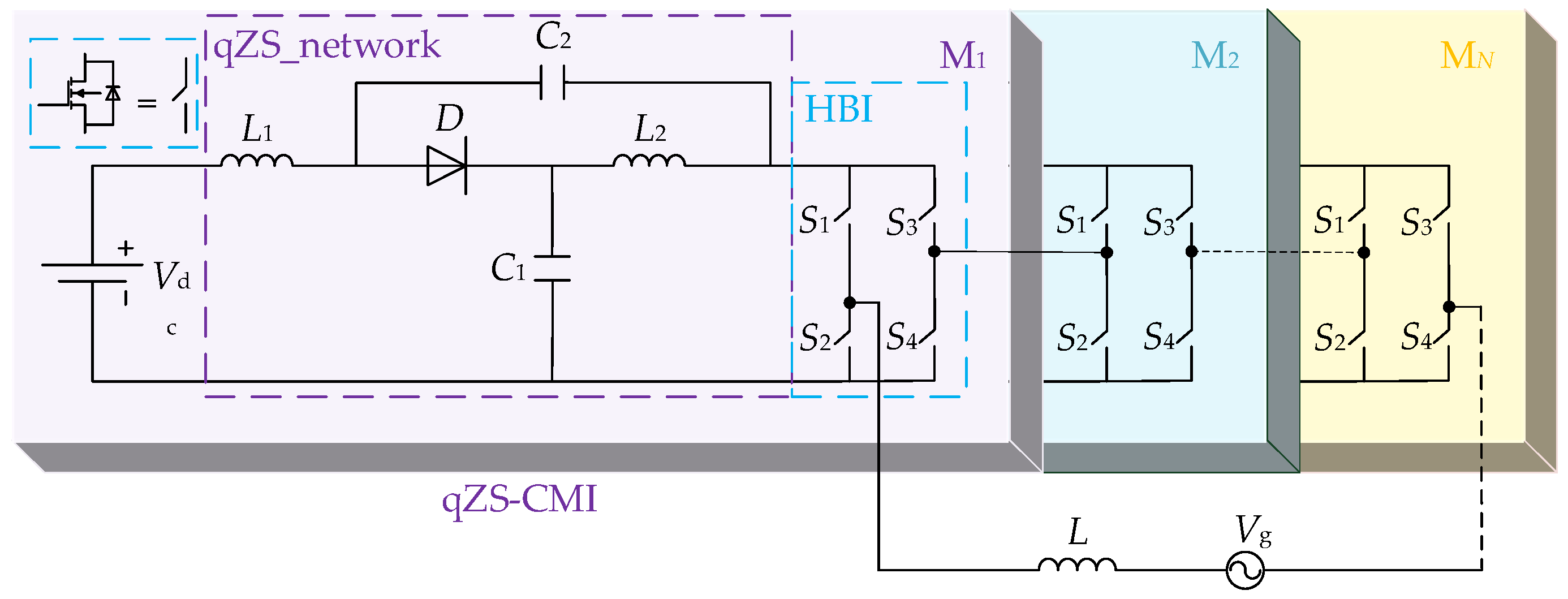
The topology of a quasi-Z-source cascaded multilevel inverter, shown in Figure 1, is a cascade of N such identical units which consists of a qZS_network in the front stage and an HBI in the back stage. A qZS_network is a quasi-Z-source inductance and capacitance network which completes the voltage boost on the DC side. An HBI is an H-bridge composed of electronic devices which completes the DC/AC inverter, L represents the filter inductance on the power grid side, and vg represents the power grid voltage.

2.1. Voltage Boost Principle of the Quasi-Z-Source

The quasi-Z-source inverter utilizes its two operational states, namely, the shoot-through state and non-through state, to achieve its intended functionality. In steady-state operation, the inverter bridge can be considered equivalent to a current source. Figure 2 below depicts the steady-state equivalent circuit diagram of the quasi-Z-source inverter.
When operating in the shoot-through state, the diode is in reverse cutoff mode, causing the capacitor to discharge. Simultaneously, both the DC power supply and the capacitor charge the inductor. In contrast, when functioning in the non-through state, the diode enters an on state while discharging the inductor. At this time, both the DC power supply and the inductor charge the capacitor while providing power to load. By analyzing these two states comprehensively, we can establish a relationship as shown by Equation (1):
v C 1 = 1 D 0 1 2 D 0 V i n v C 2 = D 0 1 2 D 0 V i n V dc = v C 1 + v C 2 = 1 1 2 D 0 V i n
where the voltages at both ends of capacitors C1 and C2 are represented by vC1 and vC2, respectively. D0 denotes the shoot-through duty ratio, Vin represents the input voltage of the DC power supply, and Vdc signifies the DC chain voltage.

2.2. Principle of Cascaded Multilevel Inverter

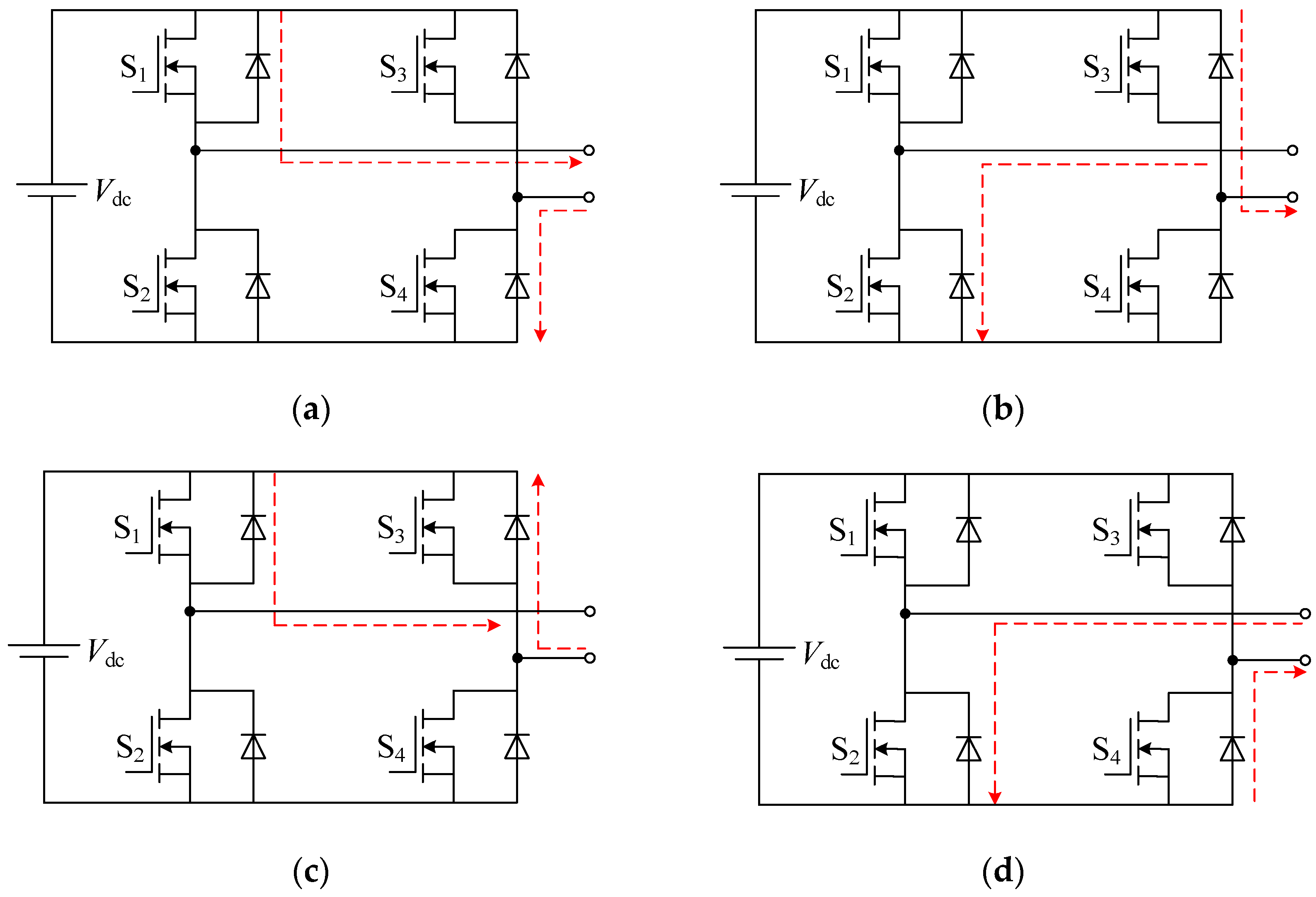
In this system, the cascaded units of the quasi-Z-source cascaded multilevel inverter are independent of each other and cascaded by the circuit shown in Figure 3. This ensures that the cascaded superposition circuit can remain unimpeded when the H-bridge circuit outputs any current level, and the H-bridge circuit of each unit has four basic working states.
When switch tubes S1 and S4 are turned on, the H-bridge is in the forward conduction state, resulting in a positive output voltage of E; when switch tubes S2 and S3 are turned on, the H-bridge operates in reverse mode, generating a negative output voltage of −E. When switches S1 and S3 are turned on, the H-bridge functions as a forward bypass with zero output voltage, allowing current to flow forward; when switch tubes S2 and S4 are turned on, the H-bridge acts as a reverse bypass with zero output voltage while enabling current to flow in reverse. The CMI working states are shown in Figure 4. A CMI can work normally only when the above four working states exist simultaneously, which is also an important feature that distinguishes cascaded multilevel inverters from clamped inverters.

2.3. QZS-CMI Mathematical Model

The mathematical model of the quasi-Z-source cascaded multilevel inverter, based on its principle, is established as follows. Firstly, the essence of the cascaded H-bridge inverter is to connect multiple H-bridges in series and realize multilevel output through the four-quadrant operation of the H-bridge inverter. Consequently, the output voltage vo can be expressed as the summation of each module’s output voltage:
v o = i = 1 N v d c i S i
where vdci is the DC chain voltage of module i, defined as Si (i = 1, 2, 3… N), which is a switching function that meets the following condition:
S i 1 , 0 , 1
Moreover, if the modulation ratio of each quasi-Z-source module is denoted as Mi, the expressions for both the output voltage voi and the total output voltage vo of module i can be derived from Equation (4):
v o i = v d c i M i sin ( ω t ) v o = i = 1 N v o i
where ω is the angular frequency of the voltage on the grid side. Since qZS-CMI is generally used in small- and medium-power situations, it can be approximately considered that the output reactive power of the AC side is zero; that is, the power factor angle is equal to zero.
Set the grid voltage and current amplitude to Vg and Ig. Then, the instantaneous value of the grid voltage and current can be expressed as
v g = V g sin ( ω t ) i g = I g sin ( ω t )
In addition, a single inductor filter is used at the grid side. The value of the filter inductance is set as L; then, the following can be obtained from KVL:
v o = L d i g d t + v g
where the instantaneous values of power grid voltage and current are represented by vg and ig, respectively, while the output voltage of the inverter is denoted as vo.

3. Current-Predictive-Control-Improved Deadbeat Current Control

3.1. Principle of Deadbeat Current Control

Deadbeat current control (DBC) is a control technique that utilizes a mathematical model of the circuit to accurately predict the value of the next sampling period based on the current system state. In comparison to other control methods, it offers advantages such as rapid response, minimal computation requirements, and stable switching frequency. By employing the forward Euler approximation formula and assuming a sufficiently small sampling period, we can derive the following equation by rewriting Equation (6):
v o ( k ) = L T s ( i g ( k + 1 ) i g ( k ) ) + v g ( k )
where Ts is the sampling period, vo(k) is the sampling value of the inverter output voltage at the current moment, vg(k) and ig(k) are the sampling values of the grid voltage and current at the current moment, and ig(k + 1) is the sampling value of the grid current at the next moment.
When the fast-tracking of the grid current is realized in a sampling period,
i g ( k + 1 ) = i ref ( k )
where iref(k) is the grid current reference value.
The inverter output voltage reference value voref(k) can be obtained by substituting Equation (8) into Equation (7):
v oref ( k ) = L T s ( i ref ( k ) i g ( k ) ) + v g ( k )
For single-phase inverters with SPWM, the modulation ratio Mi can be expressed as
M i ( k ) = v oref ( k ) v d c ( k )
For the cascaded inverter, since the cascade is a topology that connects H-bridges by N in series to achieve multilevel output, if the input power of each H-bridge power module is balanced, the modulation ratio of each H-bridge module is
M i ( k ) = v oref ( k ) N v d c i ( k )
where vdci(k) is the output voltage of the H-bridge module i at the current time, and N is the total number of H-bridge modules.
The above process is the DBC principle of grid-connected current using cascaded inverters. The general idea is to predict the reference value of the inverter output voltage at the k’th moment by referring to the reference value of the grid-connected current, and then obtain the modulation signal Mi.

3.2. Improved Deadbeat Current-Predictive Control

The traditional DBC requires that the grid-connected current can track the reference without static error in a sampling period; that is, the current deviation ie is zero. However, due to the inherent delay of the digital system, the current deviation cannot become zero in a sampling period. To realize the grid-connected current fast-tracking reference current, this study adopts an improved grid-connected current deadbeat predictive control.
Equation (7) can be deduced one step further:
v oref ( k + 1 ) = T s L ( i g ( k + 2 ) i g ( k + 1 ) ) + v g ( k + 1 )
The current deviation at time k and time k + 1 is defined as
Δ i g ( k ) = i g ( k + 1 ) i g ( k )
Δ i g ( k + 1 ) = i g ( k + 2 ) i g ( k + 1 )
The requirement of DBC ∆ig(k + 1) = 0 is relaxed, and ∆ig(k + 1) is equal to the arithmetic mean of the root of the current deviation at two adjacent moments at k + 1; that is,
Δ i g ( k + 1 ) = 1 2 Δ i g ( k + 1 ) + Δ i g ( k ) = 1 2 ( i g ( k + 2 ) i g ( k ) )
The predicted value of the output voltage of the inverter can be obtained by substituting Equation (15) into Equation (12):
v oref ( k + 1 ) = T s 2 L ( i g ( k + 2 ) i g ( k + 1 ) ) + v g ( k + 1 )
The grid voltage at time k + 1 in Equation (16) can be obtained by linear extrapolation:
v ^ g ( k + 1 ) = 2 v g ( k ) v g ( k 1 )
The modulation ratio Mi of each H-bridge module can be expressed as
M i ( k ) = v oref ( k + 1 ) N v d c i ( k )
The current closed-loop control block diagram, as depicted in Figure 5 below, is established for the aforementioned enhanced deadbeat current control strategy.
The system’s responsiveness is analyzed using the above-mentioned system control block diagram. In the figure, Ts represents the sampling period of the system; G1(z) denotes the deadbeat controller, with K being the ratio between actual and given inductance values; Z−1 signifies inherent delay in digital systems; ZOH stands for zero-order holder; and G2(z) represents the filter inductance on the output side. The role of the zero-order holder within this system is to substitute discrete digital signals with continuous analog signals; its transfer function can be expressed as
G Z ( s ) = 1 e s T s s
where Ts indicates the system sampling period.
The frequency domain transfer function of the zero-order holder and the actuator are discretized together in discrete systems, resulting in G2(z) in the discrete domain. The transformation process is illustrated by Equation (20).
G 2 ( z ) = T s L ( 1 z - 1 ) Z [ 1 s 2 ] = T s L 1 ( z 1 )
According to the aforementioned conclusions, the forward transmission function of the system can be derived as follows:
G ( z ) = G 1 ( z ) z - 1 G 2 ( z ) = K 2 z ( z 1 )
The characteristic equation of the system is obtained:
F ( z ) = 2 z 2 2 z + K = 0
The Jury stability criterion for second-order discrete systems is as follows:
a 2 + a 1 + a 0 > 0 a 2 a 1 + a 0 > 0 | a 0 | <   a 2
The above equation features the leading coefficients of the characteristic equation arranged in descending order of power, namely, a2, a1, and a0.
Based on the substitution of a2 = 2, a1 = −2, and a0 = K into the equation of the Jury stability criterion, the conclusion can be drawn that the system is stable at 0 < K < 2. Under the same conditions, the stability region of the traditional deadbeat current control is 0 < K < 1.
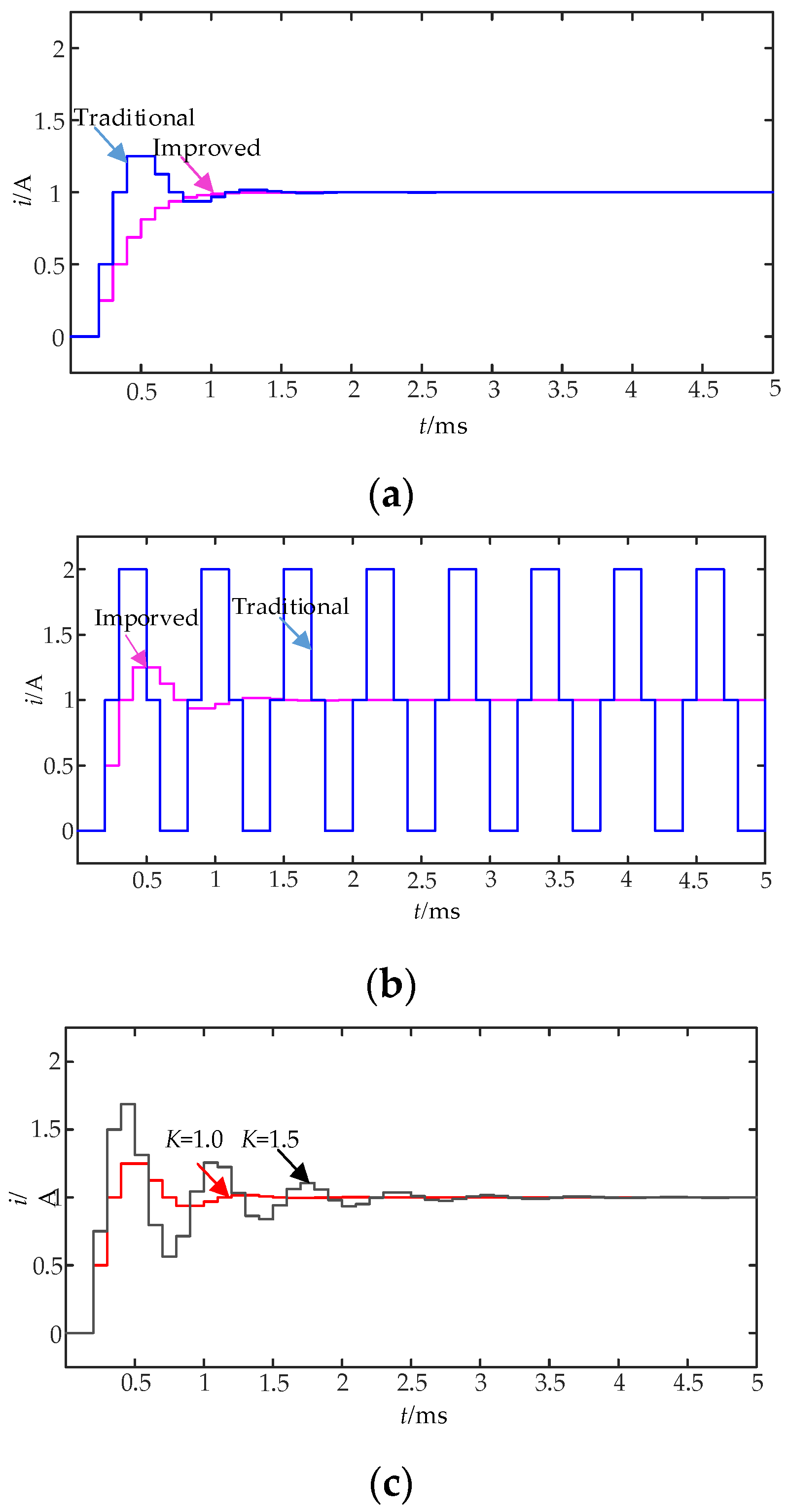
The rapidity and stability of the improved deadbeat algorithm were verified in the MATLAB/Simulink (2022b) simulation environment, disregarding the disturbance of the load voltage at the rear stage. The simulation results are presented in Figure 6.
According to the simulation results in Figure 6a, it is evident that the improved deadbeat control algorithm demonstrates faster reference tracking without any overshoot, thereby significantly improving its speed compared with the traditional deadbeat algorithm. Figure 6c validates the stability of the improved deadbeat algorithm. However, as K increases, both systems overshoot and transition time also increases. Hence, this indirectly demonstrates that the deadbeat algorithm imposes higher accuracy requirements on the system model. As depicted in Figure 6b, when K = 1, the traditional deadbeat algorithm achieves critical stability while the improved deadbeat algorithm attains a state of basic stability, indicating an enhancement in stability relative to the traditional one.

3.3. Parameter Identification of Grid-Side Inductance Based on the Least Squares Method

From the analysis of the previous section, it can be seen that as a special model of predictive control, the effect of deadbeat current-predictive control is closely related to the accuracy of the established mathematical model. If the actual inductance is too large, there will be a steady-state error ie between the grid-connected current and the reference current, and the value of ie will increase with the increase in the inductance value. If the actual inductance value is small because the inductance mainly starts to filter, a too-small inductance value will cause the harmonic distortion rate of the grid-connected current to be too large, which cannot meet the requirements of grid connection. The above two situations will lead to the control failure of the grid-connected inverter, so when the above two situations occur, the inverter needs to stop working to prevent its impact on the large power grid. In this study, by adding the parameter identification of the filter inductance value, the change in the inductance value is monitored in real time to avoid the above situation.
The least squares method is currently widely used in system parameter estimation because of its simple and easy-to-understand advantages. However, in practical applications, the recursive least squares method will have the phenomenon of data saturation, leading to algorithm failure. To overcome these limitations, and to dilute the influence of old data on new data while improving the influence of new data, this study adopts recursive least squares with forgetting factor (FRLS) and its value function is
J = k = 1 n λ ( n k ) [ y ( k ) ϕ T ( k ) θ ^ ( k ) ] 2
where y(k) is the output matrix, ϕ(k) is the input matrix, and θ(k) is the parameter matrix to be identified, among them y ( k ) = ϕ ( k ) θ ( k ) . In this study, y(k) = [ig(k + 1) − ig(k)], ϕ(k) = [vo(k) vg(k)], θ(k) = [G -G]T, where G = L/Ts.
Combined with the derivation of the recursive least squares method, the FRLS iteration equation is
θ ^ ( k ) = θ ^ ( k 1 ) + K ( k ) [ y ( k ) ϕ T ( k ) θ ^ ( k 1 ) ] K ( k ) = P ( k 1 ) ϕ ( k ) λ + ϕ T ( k ) P ( k 1 ) ϕ ( k ) P ( k ) = [ I K ( k ) ϕ T ( k ) ] P ( k 1 ) / λ
where K(k) represents the number of iterations, and λ is the forgetting factor, generally 0.95~1.0. Because the FRLS algorithm needs to use the prior values of the covariance matrix P and the parameter estimation matrix θ ^ in the iterative process, P(0) and θ ^ ( 0 ) are usually given in advance. Generally, we let P(0) = δ−1I, where δ is a small real number, I is the unit matrix, and θ ^ ( 0 ) = 0 .
It can be seen from Equation (25) that when the value of λ is less than 1, as the data continue to iterate, the old data will decay exponentially, which is equivalent to adding a weight factor to the old data that decays exponentially.

4. Multi-Carrier Phase-Shifted Sinusoidal Pulse Width Modulation

Since the Z-source/quasi-Z-source inverter was proposed, modulation methods have emerged continuously. At present, for the single-phase qZS-CMI, the combination of simple boost and PSPWM is generally used as the modulation method of single-phase qZS-CMI, as shown in Figure 7a. The idea is to insert the shoot-through zero vector into the traditional zero vector in the inverter. However, the insertion of the shoot-through zero vector will double the switching frequency, resulting in an increase in switching losses, thereby reducing the efficiency of the system. To address these issues, this paper adopts an improved multi-carrier phase-shifted sinusoidal pulse width modulation (MPSPWM) approach. By adjusting the insertion time of the shoot-through vector, the switching frequency is reduced to mitigate switching losses. The improved multi-carrier phase-shifting SPWM scheme is illustrated in Figure 7b below.
The basic principle, as illustrated in the above figure, involves translating the original carrier to ensure that the two switching tubes of each bridge arm utilize distinct carriers with an amplitude difference of D0. This extension of on-time for a specific switching tube within the same bridge arm fulfills the voltage boost requirement. The driver signals G1 and G2 share a modulated wave but employ different carriers. The amplitudes of these two carriers are 1 – D0/2 and 1 + D0/2, respectively, where D0 represents the shoot-through duty ratio. The same applies to G3 and G4. While G1 and G4 share a common carrier, they adopt different modulated waves with a phase difference of 180° between them; the same is true for G2 and G3. The specific modulation method is shown in Figure 8.
In the diagram, Vc and Vr are triangular carriers and sinusoidal modulation waves with an amplitude of 1, respectively; D0 is a shoot-through duty cycle; and G1, G2, G3, and G4 are four driving signals. When Vr > (VcD0/2), the S1 output is positive, and vice versa; when −Vr > (VcD0/2), the S3 output is positive, and vice versa; when Vr > (Vc + D0/2), S2 output is positive, and vice versa; and when −Vr > (Vc + D0/2), the S4 output is positive, and vice versa.

5. Results of the System

In order to validate the accuracy of the proposed system in this study, the MATLAB/Simulink (2022b) simulation platform was utilized to construct a seven-level qZS-CMI system simulation model. The control block diagram of the model is depicted in Figure 9 and the seven-level qZS-CMI system simulation model is depicted in Figure 10.
The power level, depicted in the figure, is a cascaded multilevel quasi-Z-source inverter module; DBC refers to an enhanced grid-connected deadbeat current controller. Its operational procedure can be outlined as follows: Firstly, the load voltage, current, and DC bus voltage are sampled. To ensure that the output current remains in phase with the grid voltage, phase information of the specified current is obtained with PLL. Subsequently, four signals are transmitted to the deadbeat controller for acquiring modulation signal Mi. Finally, multi-carrier phase-shifted SPWM is employed to modulate both shoot-through signal D0 and modulated signal Mi, resulting in the generation of 12 driver signals. The specific simulation parameters are shown in Table 1.

5.1. Analysis of System Steady-State Simulation Results

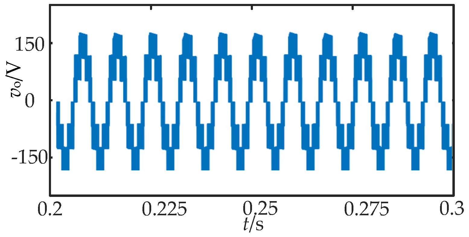
In this study, given an input DC voltage of 35 V, the DC chain voltage can be calculated as Vdc = 70 V using Equation (1). Consequently, it is evident that the peak value of the inverter’s output voltage is Vo = N × Vdc = 210 V. For the simulation, Figure 11 illustrates the output seven-level AC voltage of the inverter, while Figure 12 depicts the waveform diagram of the DC chain voltage for any Z-source module. The obtained values align with theoretical expectations, thereby validating the accuracy and feasibility of the qZS-CMI mathematical model.
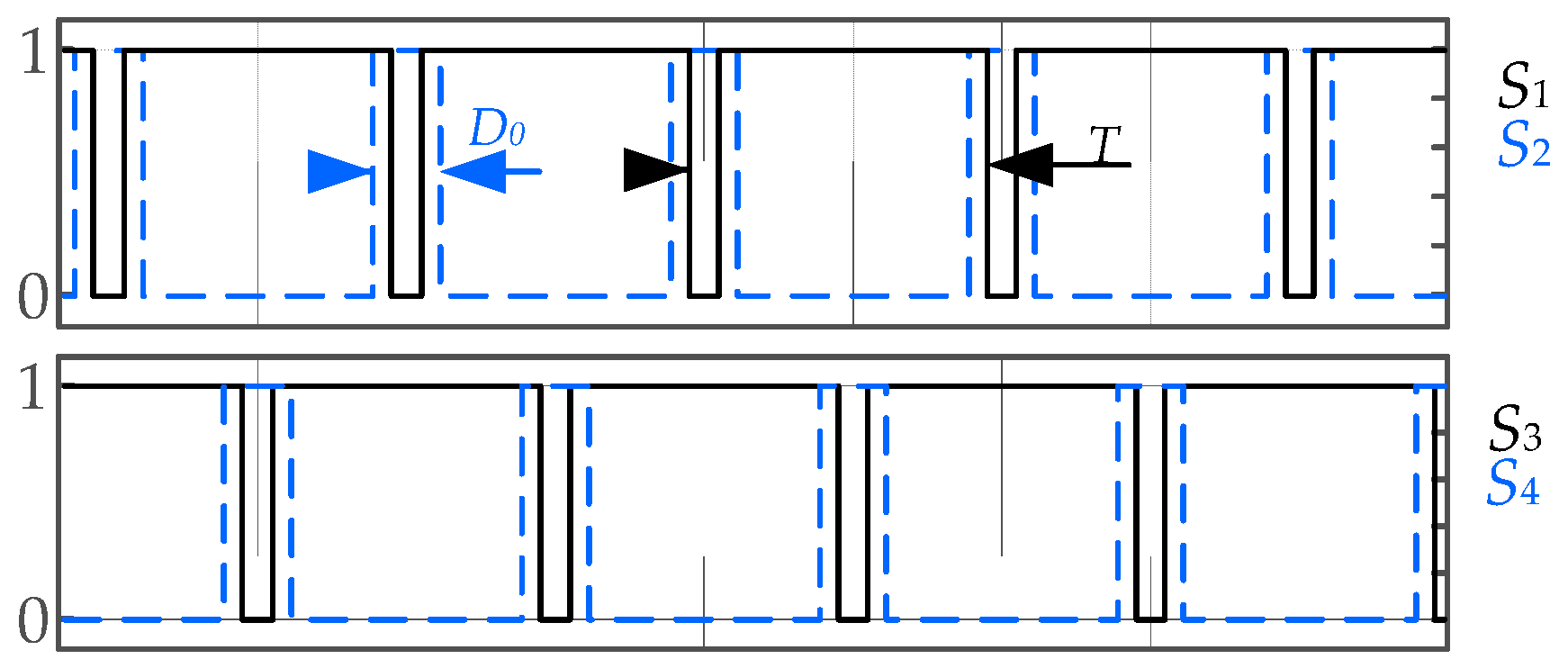
The driving signal of a qZS-CMI module is illustrated in Figure 13 below, with a fixed duty ratio set at 0.25. Following multi-carrier phase-shifted modulation, the shoot-through zero vector is divided into four segments and incorporated into the switching state. As a result, there will be four shoot-through zero states within each switching cycle, with each direct-zero state lasting for D0/4 duration.
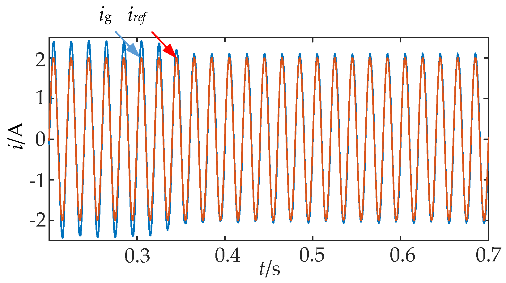
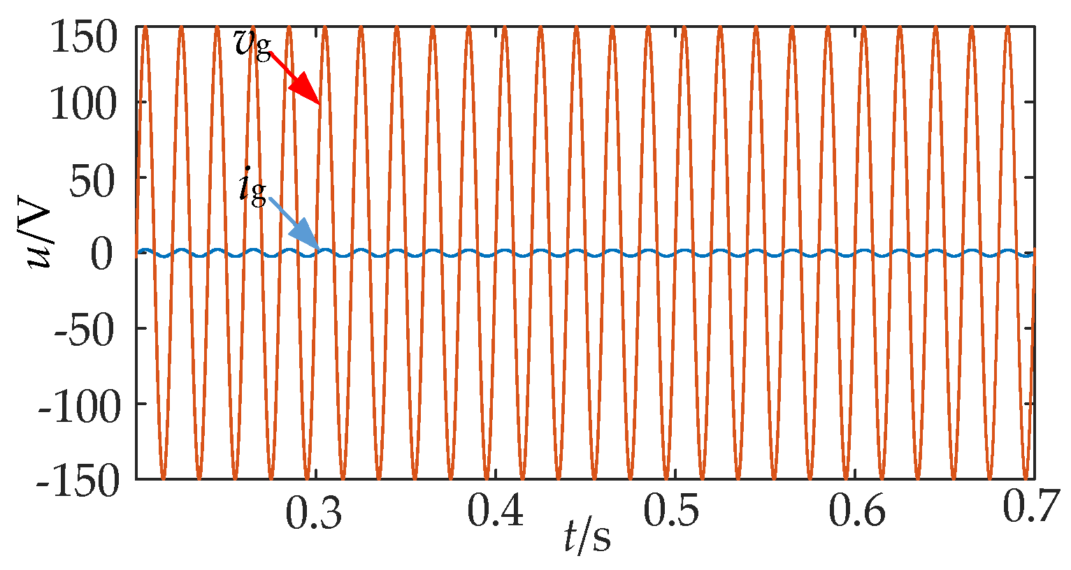
The current waveform at the grid side is illustrated in Figure 14, demonstrating that the current successfully tracks the set value after approximately 0.35 s, thereby validating the efficacy of the proposed enhanced deadbeat current control method in this study. Additionally, the current at the grid side exhibits phase alignment with the grid voltage, as depicted in Figure 15.
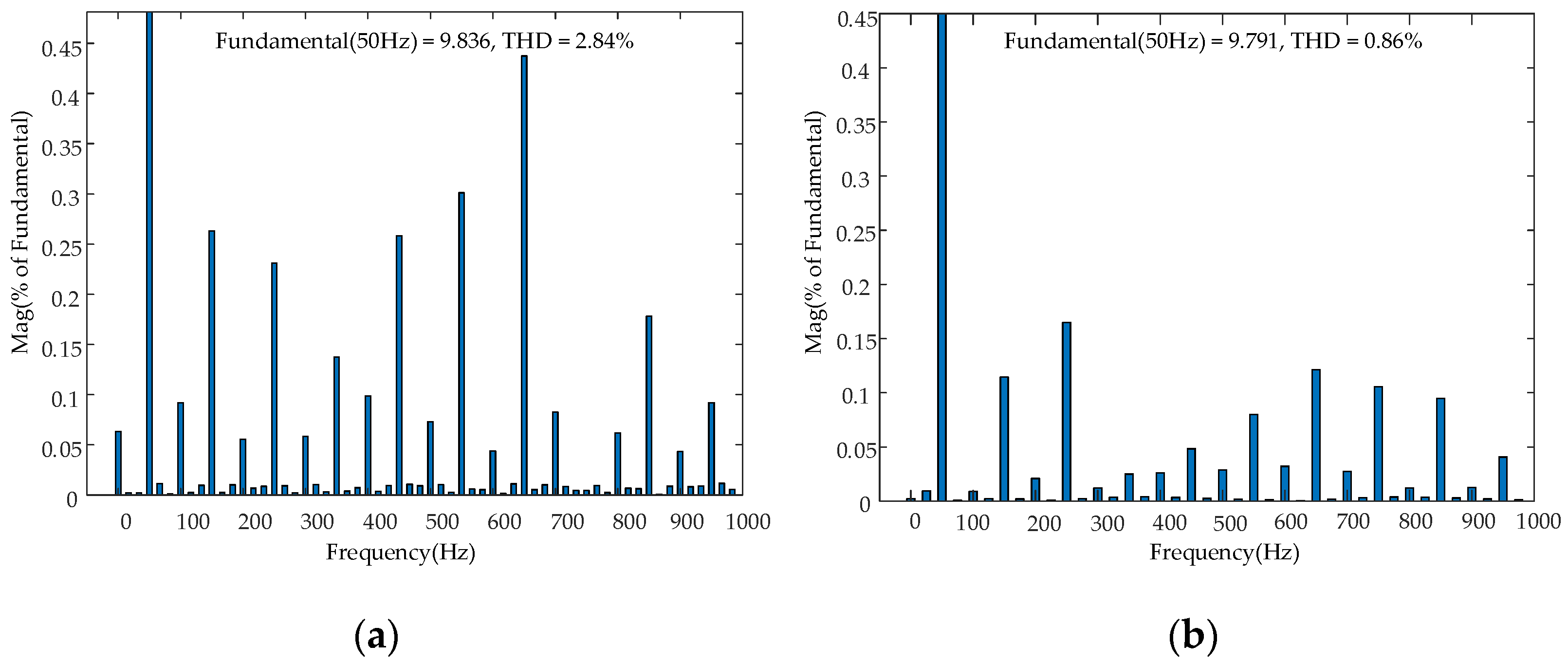
Figure 16 illustrates the total harmonic distortion (THD) of the grid side using both traditional and improved deadbeat control algorithms, which resulted in rates of 2.55% and 0.86%, respectively. It is evident that the deadbeat control algorithm effectively reduces the THD of the grid-connected current.
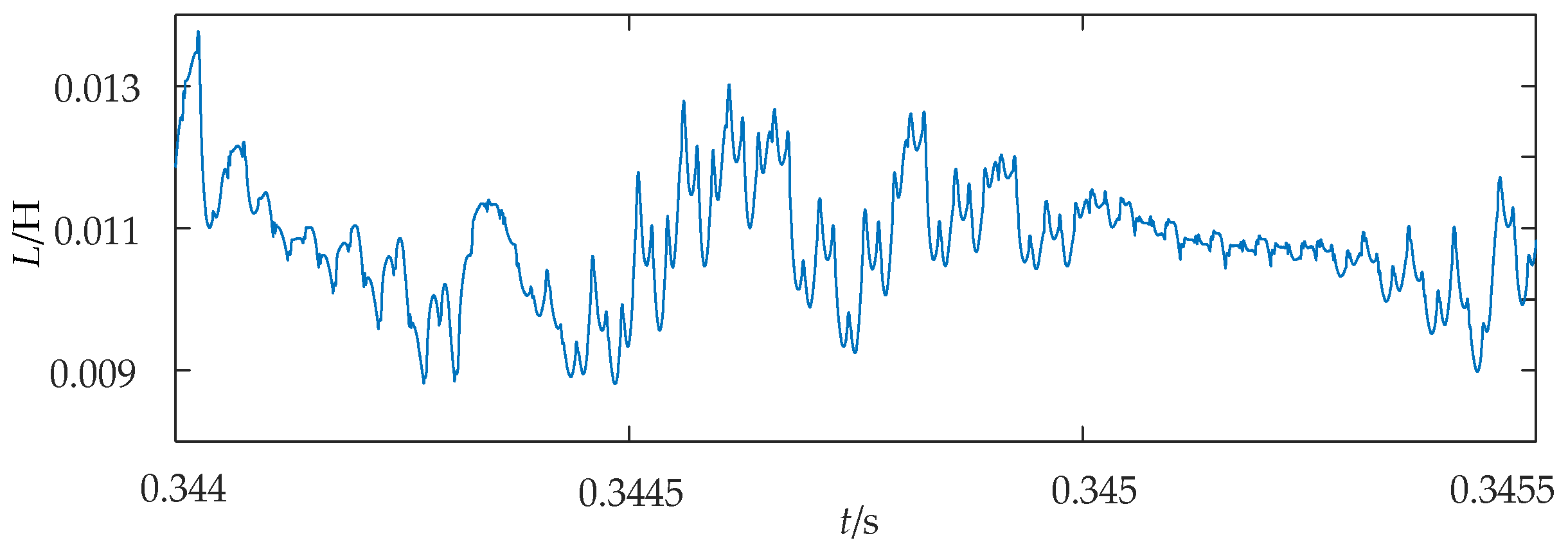
Figure 17 shows the estimated value of the filter inductance. Combined with Figure 14 and Table 1, it can be seen that the FRLS algorithm can undertake the parameter identification of the qZS-CMI filter inductance.
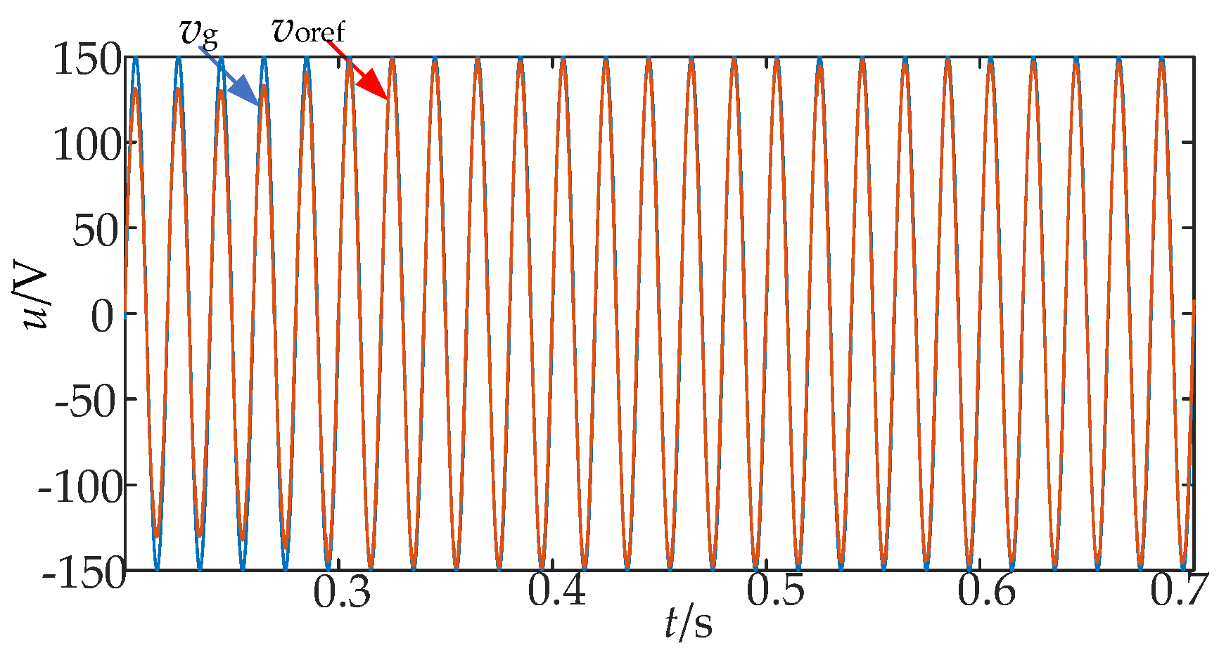
According to Equation (7), the output voltage voref(k + 1) predicted by the deadbeat algorithm, after the system reaches a steady state, should be equal to the grid voltage vg(k + 1). Figure 18 illustrates the waveform diagram of the output voltage predicted by the deadbeat algorithm and the grid-side voltage.
The voltage voref, as depicted in Figure 18, exhibits excellent tracking capability with the grid-side voltage vg once the system reaches a steady state. This ensures precise modulation ratio M and satisfies the coupling relationship between the modulation ratio and shoot-through duty ratio.

5.2. Analysis of System Dynamic Simulation Results

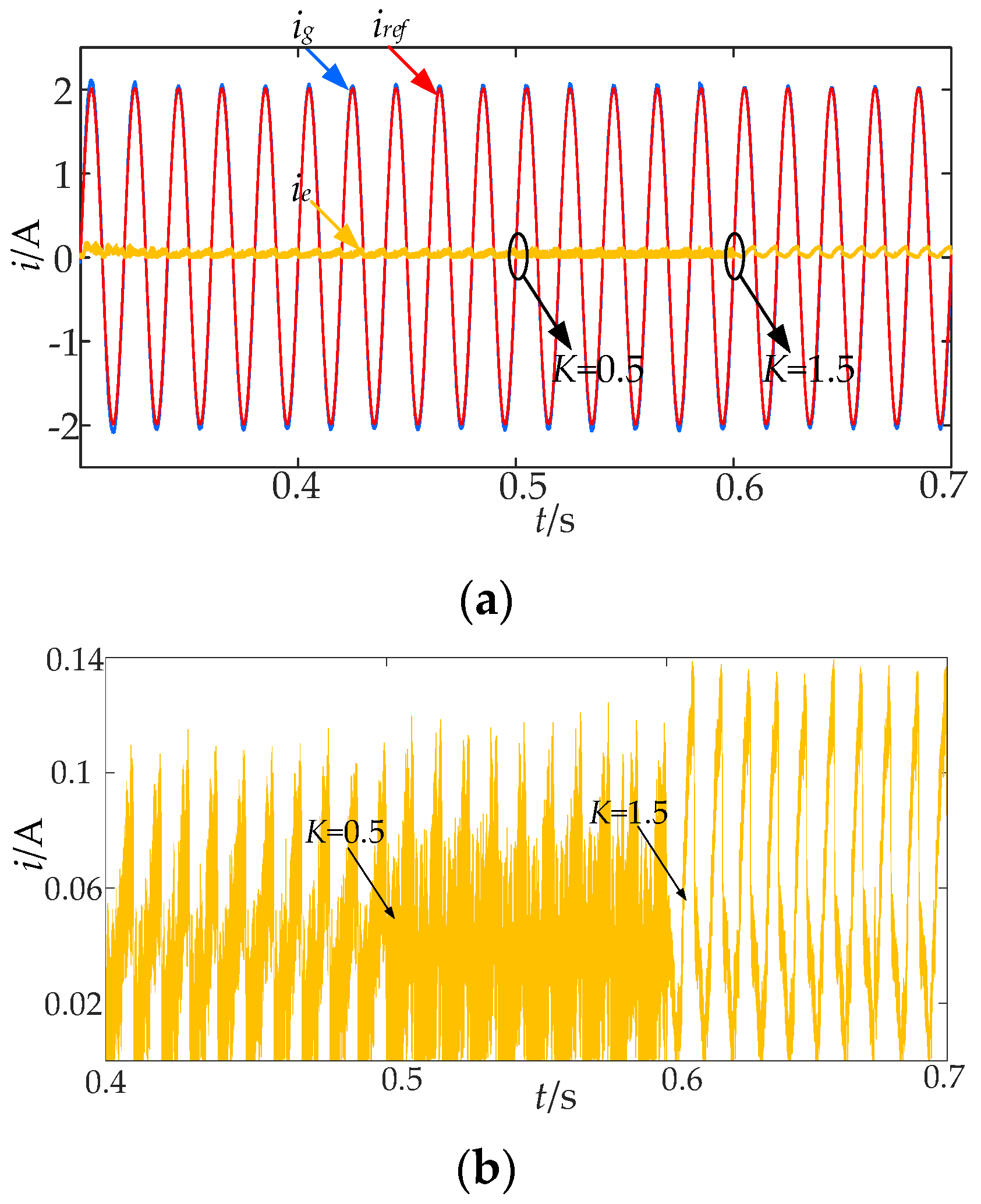
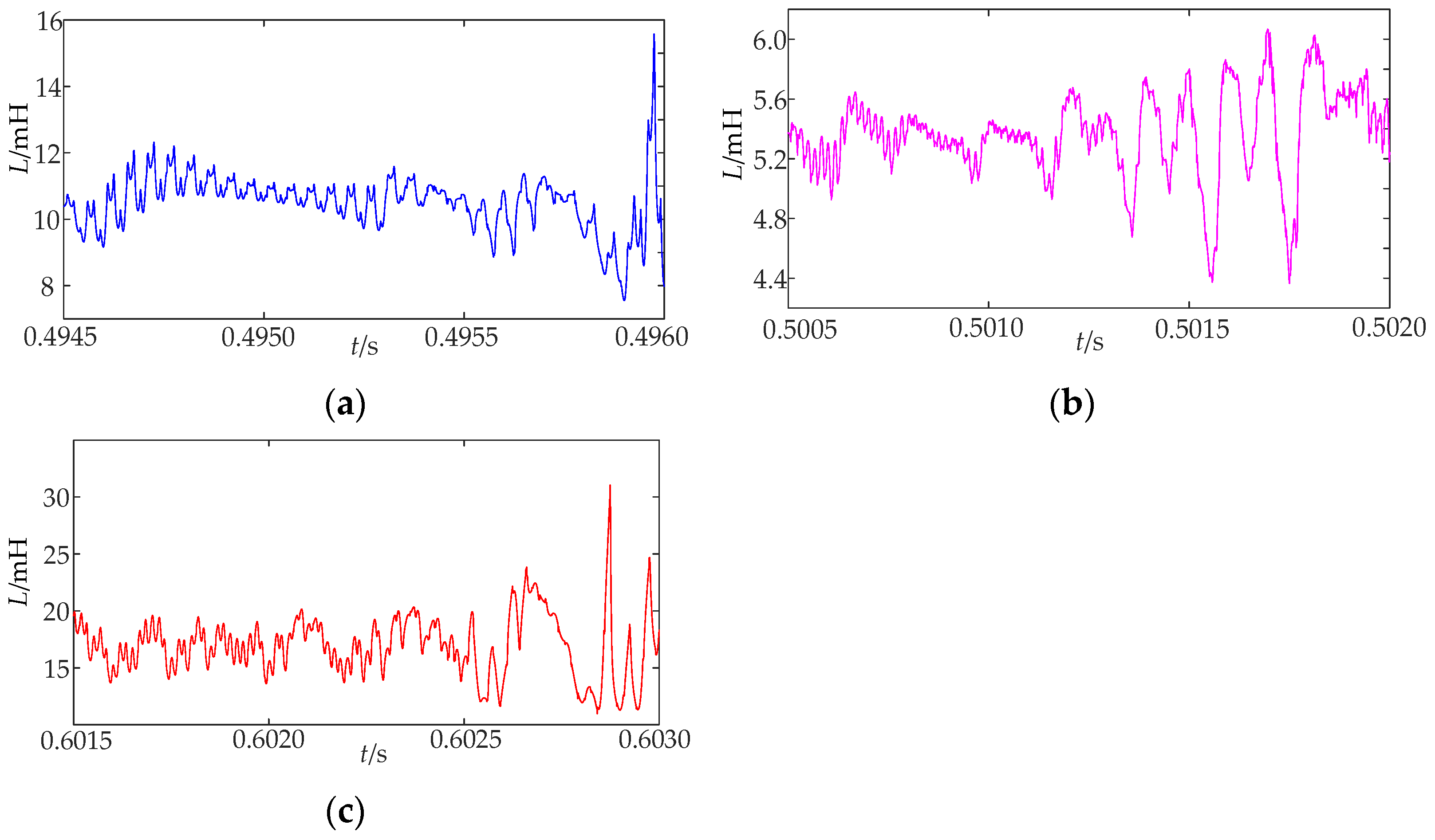
To verify the stability of the improved deadbeat current-predictive control, the grid-side inductance is reduced at 0.5 s, and the grid-side inductance is increased at 0.6 s; that is, at 0.5 s, K = 0.5, and at 0.6 s, K = 1.5. Figure 19 and Figure 20 provide the grid-connected current waveform and the grid-side inductance value identified using the FRLS algorithm.
Figure 19a,b shows the process of grid-connected current tracking the given current under the fluctuation of grid-side inductance and the absolute value of the difference from the grid-connected current, respectively. It can be seen that the grid-connected current can effectively track the given value, and the grid-connected current has no obvious fluctuation in the case of grid-side inductance fluctuation, and its dynamic error fluctuates between 0 and 0.14 A. In addition, between 0.5 s and 0.6 s in the local amplification diagram, the harmonic component of the grid-side current increases because the filter inductance value is reduced to half of the original value. After 0.6 s, because the filter inductance value increases to 1.5 times the original, ie increases; that is, the system overshoot increases and tends to be critically stable. The above simulation results verify well the content discussed in Section 3.2.
Figure 20 shows the inductance values identified using the FRLS algorithm in the process of grid-side inductance fluctuation. From the change curves in Figure 20a–c, it can be found that the FRLS algorithm has a large overshoot; in particular, when the inductance value increases, the overshoot is more obvious, about 10 mH. This also shows that the FRLS algorithm is sensitive to noise.
In addition, since the improved DBC strategy in this study does not add a voltage loop, it is necessary to verify the change in grid-connected current when the input voltage changes.
After the system enters the steady state, a 2.5 V step signal is applied to the input voltage Vdc at 0.5 s. Figure 21 and Figure 22 present the waveforms of the grid-connected current and the DC link voltage when the input voltage changes.
From the simulation results in Figure 21a,b, it can be seen that when the input voltage fluctuation system re-transitions to a steady state, the grid-connected current produces a small overshoot with a value of about 0.06 A, but after one quarter of the cycle, that is, 0.005 s, it can re-enter the steady state. Figure 22 shows that the DC link voltage jumps to 75 V at this time. In addition, since the capacitor voltage cannot mutate and the inductor current cannot mutate, the DC link voltage does not jump immediately when the input voltage fluctuates. Therefore, for a grid-connected system with a relatively stable input voltage, the improved DBC does not need to adopt double closed-loop control, which also simplifies the design of the control link to a certain extent.

5.3. Analysis of Experimental Results

According to the design parameters listed in Table 1, this study constructed a seven-level qZS-CMI experimental platform with a power rating of 0.75 kW. The obtained experimental data were essentially consistent with the simulation results, which further validated the accuracy and feasibility of the system. The main parameters of the experimental platform are shown in Table 2; for other parameters, refer to the simulation section.
Figure 23a presents the DC link voltage waveforms of three independent qZS-HBI modules. The three DC link voltages can remain stable and the peak values are equal to about 70 V. When the shoot-through duty cycle is 0.25, as mentioned in Section 5.1, the peak value of the DC link voltage should be 70 V. The waveform in Figure 23a is just consistent with the theoretical calculation value. Figure 23b shows the voltage waveform of the capacitor C1 in the quasi-Z-source network of three independent qZS-HBI modules. According to the setting value of the shoot-through duty cycle and the input voltage parameters in the program and Equation (1), the peak value of the voltage of the capacitor C1 is 60 V, while the peak value of the capacitor voltage waveform shown in Figure 23b is basically stable at 60 V; therefore, the theoretical analysis is consistent with the experimental results, and the capacitor voltage waveform is continuous.
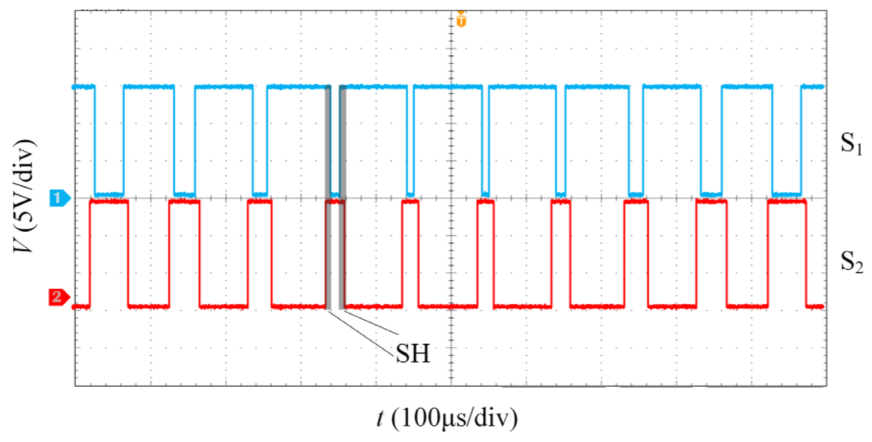
Figure 24 shows the measured waveforms of the driving signals of the upper and lower switches S1 and S2 of the same bridge arm in a qZS-HBI module. MPSPWM control inserts the shoot-through zero vector into the switching moment, that is, the shadow part in Figure 24, which is roughly one-eighth of the switching period. The amplitude of its high level is 10 V, which can effectively drive MOS.
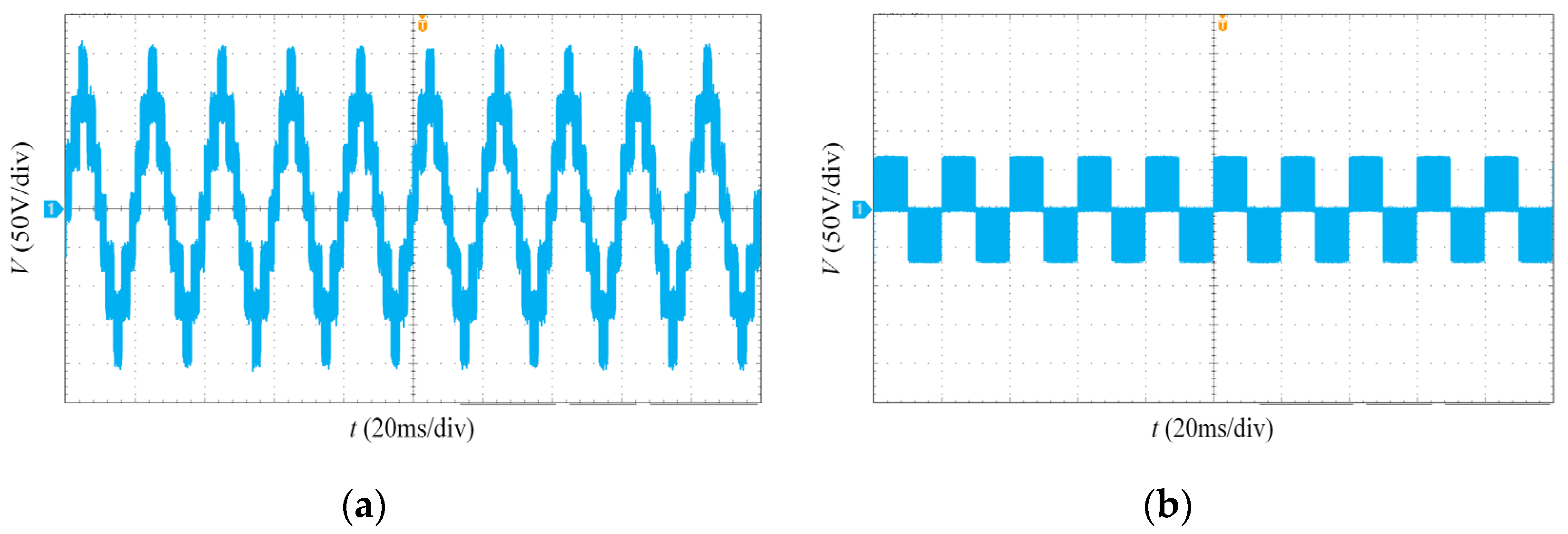
The output voltage waveform of the qZS-CMI prototype system is depicted in Figure 25a prior to filtering. Upon reaching steady state, the peak voltage waveform stabilizes at approximately 210 V, exhibiting a seven-level sine wave pattern. By referring to Table 2 for input voltage parameters and observing the waveform in Figure 25a, it can be inferred that the qZS-CMI prototype system effectively achieves a six-fold boost output. Furthermore, to ensure continuous current flow within the cascade structure, it is essential to ascertain the output level of an individual qZS-HBI module. Figure 25b illustrates the output voltage waveform of qZS-HBI module 1. As in the Section 2.2 analysis, maintaining current path necessitates four distinct operating states for each qZS-HBI module; thus, its output voltage should manifest as a three-level waveform. The voltage waveform presented in Figure 25b indeed exhibits this three-level characteristic with a peak voltage around 70 V, aligning with both theoretical analysis and the DC chain voltage of an individual qZS-HBI module.
Figure 26a,b below show the grid-connected current waveforms under the control of the traditional deadbeat algorithm and the improved deadbeat algorithm, respectively. According to the requirement of dynamic stability in a power system, the power system should be able to restore the original operation state or transition to a new stable operation state after being disturbed. As shown in Figure 26, when the load fluctuates, the system transitions to a new stable operating state. The output current under the traditional deadbeat control enters a stable state after about 40 ms, while the output current under the improved DBC enters a stable state after about 4 ms. This proves well the rapidity of the improved deadbeat control. Also, the current fluctuation in Figure 26a is large, whereas the current fluctuation in Figure 26b demonstrates a minor amplitude and closely resembles a sine wave. Therefore, it can be concluded that the power quality obtained under the improved DBC is higher than that under the traditional control, which can meet the requirements of grid connection. Therefore, the superiority of the current-predictive control method used in this paper is further proved.
Figure 27 below provides the voltage and current waveforms of the load after filtration. In this figure, both voltage and current have amplitudes approximately equal to 150 V and 10 A, respectively, while their effective values are measured as 106.1 V and 7.1 A. The output power is determined as 0.753 kW, with voltage and current being in phase exhibiting sinusoidal variations.

6. Conclusions

In this article, the principle of a quasi-Z-source cascaded multilevel photovoltaic inverter is expounded firstly, and the mathematical model of a qZS-CMI is established. Then, an improved deadbeat control strategy is proposed to solve the problems of switching frequency doubling and high harmonic rate on the grid side. The main features are as follows:
(1) It replaces the traditional ‘Boost + inverter’ two-stage structure with a quasi-Z-source inverter to achieve a single-stage boost inversion.
(2) Considering the characteristics of photovoltaic distributed power generation systems and the susceptibility of photovoltaic cells to environmental factors, a cascaded multilevel inverter (CMI) is adopted to significantly reduce the power burden on all joint units, while the overall system’s quality and efficiency are enhanced with the independent maximum power point tracking of each power unit.
(3) The current-predictive control strategy is introduced and improved to mitigate current harmonics caused on the grid side by the constant charging and discharging of the quasi-Z-source network.
(4) An improved multi-carrier phase-shifted sinusoidal PWM method is proposed as a solution to the problem of frequency doubling due to shoot-through zero vector insertion for the purpose of single-stage boost. This method inserts the shoot-through zero vector into switching time intervals, aiming to reduce switching frequency and minimize switching losses.
(5) In order to ensure the reliability and stability of the control, the FRLS is introduced to identify the parameters of the grid-side filter inductor, which can prevent the control failure caused by the change of the grid-side parameters, so as to realize the real-time monitoring of the grid-side current.
In forthcoming research, system efficiency and quality will be further enhanced in the method’s application to photovoltaic power generation systems. The method can also be applied to motor drive and control to improve the operational properties.

Author Contributions

Conceptualization, N.J. and J.J.; methodology, N.J. and J.J.; software, S.L. and J.J.; validation, S.L. and J.J.; supervision, N.J.; writing—original draft, S.L.; writing—review and editing, S.L. and N.J. All authors have read and agreed to the published version of the manuscript.

Funding

This research was funded by China’s Training Program of Innovation and Entrepreneurship for Undergraduates, grant number 202310214160.

Data Availability Statement

Data are contained within the article.

Conflicts of Interest

The authors declare no conflicts of interest. The funders had no role in the design of the study; in the collection, analysis, or interpretation of data; in the writing of the manuscript; or in the decision to publish the results.

References

  1. Peng, F.Z. Z-source inverter. IEEE Trans. Ind. Appl. 2003, 39, 504–510. [Google Scholar] [CrossRef]
  2. Lu, H.C. Research on Permanent Magnet Synchronous Motor System Based on Three-Level Inverter and LC Filter; Huazhong University of Science and Technology: Wuhan, China, 2022. [Google Scholar]
  3. Zhang, C.H.; Zhou, J.W.; Du, C.S.; Chen, A.L. Review of Control Strategies of Single-phase Cascaded H-Bridge Multilevel Inverter for Grid-connected Photovoltaic Systems. J. Power Supply 2017, 15, 1–8. [Google Scholar]
  4. Xu, J.; Xu, T.L. Research on NPC Single-Phase Inverter Based on Five-Level Control. Sol. Energy 2021, 15, 1–8. [Google Scholar]
  5. Dong, S.; Zhang, Q.F.; Wang, R.; Wang, H.L.; Cheng, S.K. Development of the Z-Source Inverters and Its Key Technologies: A Review. J. Electr. Eng. 2016, 11, 1–12. [Google Scholar]
  6. Su, H.S.; Lin, H.J.; Che, Y.L. Comparative Analysis of All Kinds of Z-source Inverters in Properties and Their Application Background. Control Eng. China 2017, 24, 188–196. [Google Scholar]
  7. Li, S.; Si, W.X.; Chen, Y.; Cui, S. Research on Isolated Quasi-Z-Source Single Phase Photovoltaic Grid Connected Inverter Based on PR Control. Acta Energiae Solaris Sin. 2018, 39, 3081–3089. [Google Scholar]
  8. Zhang, R.; Li, Y. System Parameter Design and Grid-connected Control Methods for Quasi-Z-Source Cascaded Multilevel Inverter Considering Power Difference of Modules. Proc. CSEE 2018, 48, 4836–4845. [Google Scholar]
  9. Wang, J.; Zhang, R.; Liu, Y.; Li, Y. A Multi-Modulation Waveform Phase-Shift Sinusoidal Pulse Width Modulation Method of QZS-CHI and Its Output Voltage Analysis. Trans. China Electrotech. Soc. 2020, 35, 3470–3477. [Google Scholar]
  10. You, Y.F.; Li, Y.; Xiao, X.Y.; Fang, F. Finite control set-model predictive control of single-phase quasi-Z-source cascaded multilevel inverter. Power Syst. Prot. Control 2020, 48, 1–8. [Google Scholar]
  11. Niu, L.; Yang, M.; Liu, K.S.; Xu, D.G. A Predictive Current Control Scheme for Permanent Magnet Synchronous Motors. Proc. CSEE. 2012, 32, 131–137. [Google Scholar]
  12. Yang, H.; Yang, L.H.; Chen, Y.M.; Shi, J.Z.; Wang, S.K. Deadbeat Predictive Current Control Strategy Based on Disturbance Compensation for Grid Connected Inverter with LCL Filter. Proc. CSEE 2023, 43, 1–16. [Google Scholar]
  13. Chen, Y.D.; Luo, A.; Zhou, L.M.; Xie, N.; Jin, G.B.; Lu, Z.P. A Robust Predictive Deadbeat Grid-connected Control Method Based on Power Feed-forward Control. Proc. CSEE 2013, 33, 62–70. [Google Scholar]
  14. Jiang, Y.; Xu, W.; Mu, C.; Liu, Y. Improved deadbeat predictive current control combined sliding mode strategy for PMSM drive system. IEEE Trans. Veh. Technol. 2017, 67, 251–263. [Google Scholar] [CrossRef]
  15. Qu, A.W.; Chen, D.L.; Su, Q. Simple Boost Modified Space Vector Modulation Strategy for Three-Phase Quasi-Z-Source Grid-Connected Inverter. Trans. China Electrotech. Soc. 2018, 33, 826–836. [Google Scholar]
  16. Guo, H.S. Improvement of SVPWM Direct Modulation Strategy for Quasi-Z Source Inverter. Electr. Eng. 2022, 05, 67–70. [Google Scholar]
  17. You, Y.F.; Li, Y.; Fang, F.; Yang, X.Y. Deadbeat grid-connected control strategy of quasi-Z-source cascaded multilevel inverter and System Parameter Design. Power Syst. Prot. Control 2019, 2022, 47. [Google Scholar] [CrossRef]
  18. Zhang, Y.C.; Li, B.Y.; Liu, J. Online Inductance Identification of a PWM Rectifier Under Unbalanced and Distorted Grid Voltages. IEEE Trans. Ind. Appl. 2020, 56, 3879–3888. [Google Scholar] [CrossRef]
  19. Chen, Z.G.; Yang, L.Y.; Zhang, Y.L.; Li, Z.X. A Control Method of PMSM Current-Loop Based on Online Parameter Identification; IEEE Computer Society: Singapore, 2012; pp. 417–422. [Google Scholar]
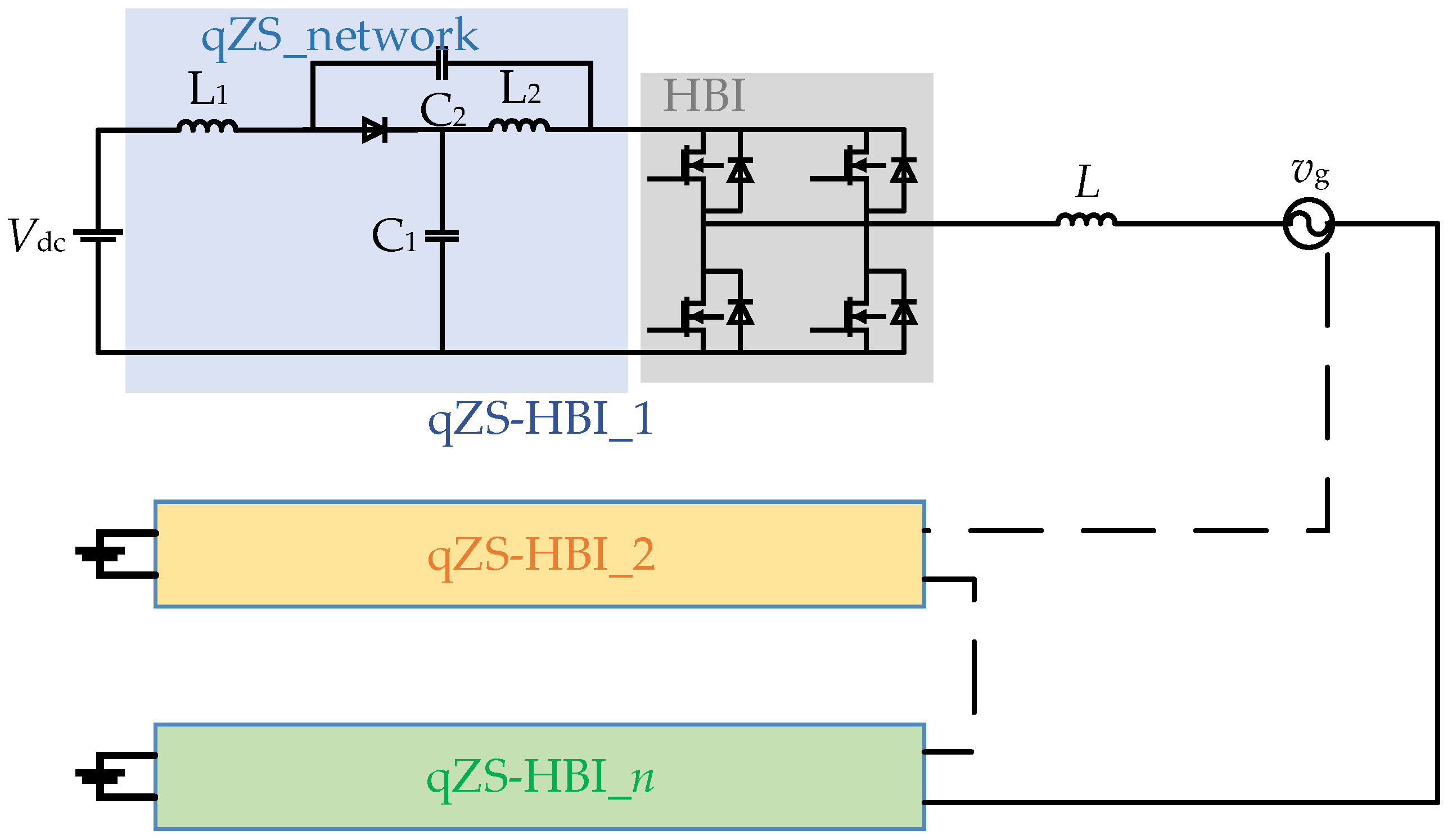
Figure 1. Diagram of the quasi-Z-source cascaded multilevel inverter.
Electronics 13 01824 g001
Figure 2. Equivalent circuit diagram of quasi-Z-source inverter.
Electronics 13 01824 g002
Figure 3. Quasi-Z-source cascaded multilevel inverter topology.
Electronics 13 01824 g003
Figure 4. CMI working states: (a) forward conduction, (b) reverse conduction, (c) forward bypass, (d) reverse bypass.
Electronics 13 01824 g004
Figure 5. System control block diagram.
Electronics 13 01824 g005
Figure 6. Simulation results of the enhanced deadbeat algorithm: (a) K = 0.5; (b) K = 1.0; (c) K = 1.0 and 1.5.
Electronics 13 01824 g006
Figure 7. (a) Simple boost modulation and PS-PWM, (b) multi-carrier phase-shifted SPWM.
Electronics 13 01824 g007
Figure 8. Multi-carrier phase-shifted SPWM modulation schematic.
Electronics 13 01824 g008
Figure 9. Block diagram of the qZS-CMI control strategy.
Electronics 13 01824 g009
Figure 10. Seven-level qZS-CMI system simulation model.
Electronics 13 01824 g010
Figure 11. Inverter output voltage.
Electronics 13 01824 g011
Figure 12. DC link voltage.
Electronics 13 01824 g012
Figure 13. Drive signals.
Electronics 13 01824 g013
Figure 14. Grid current waveform.
Electronics 13 01824 g014
Figure 15. Grid voltage and grid current waveforms.
Electronics 13 01824 g015
Figure 16. Harmonic distortion rate of grid-connected current: (a) traditional control; (b) improved control.
Electronics 13 01824 g016
Figure 17. Filtering inductance estimation.
Electronics 13 01824 g017
Figure 18. Predicted voltage waveform.
Electronics 13 01824 g018
Figure 19. Current waveform when the grid-side inductance changes: (a) grid-connected current; (b) local amplification of current dynamic error.
Electronics 13 01824 g019
Figure 20. Network-side inductance parameter identification waveform: (a) 10 mH; (b) 5 mH; (c) 15 mH.
Electronics 13 01824 g020
Figure 21. Current waveform when input voltage fluctuates: (a) grid-connected current; (b) local amplification of current dynamic error.
Electronics 13 01824 g021
Figure 22. DC link voltage when input voltage fluctuates.
Electronics 13 01824 g022
Figure 23. DC link voltage waveform: (a) DC link voltage waveform; (b) voltage waveform of the capacitor C1.
Electronics 13 01824 g023
Figure 24. Driving signal waveform.
Electronics 13 01824 g024
Figure 25. Inverter output waveform: (a) CMI output voltage waveform; (b) single HBI module output voltage waveform.
Electronics 13 01824 g025
Figure 26. The grid-connected current waveform: (a) traditional DBC; (b) improved DBC.
Electronics 13 01824 g026
Figure 27. The voltage and current waveform after filtering.
Electronics 13 01824 g027
Table 1. Main simulation parameters of qZS-CMI.
Main ParametersValues
Quasi-Z-source Inductance (H)0.003
Quasi-Z-source Capacitance (F)0.004
Input Voltage (V)35
Grid Voltage (V)150
Grid Current (A)2
Filter Inductance (H)0.01
Maximum Shoot-through Duty Ratio0.25
Switching Frequency (kHz)10
Table 2. Main parameters of qZS-CMI.
Main ParametersValues
Input Voltage (V)35
DC Link Voltage Peak (V)70
Peak Output Voltage After Filtered (V)150
Peak Output Current (A)10
Switching Frequency (kHz)10
Disclaimer/Publisher’s Note: The statements, opinions and data contained in all publications are solely those of the individual author(s) and contributor(s) and not of MDPI and/or the editor(s). MDPI and/or the editor(s) disclaim responsibility for any injury to people or property resulting from any ideas, methods, instructions or products referred to in the content.