Article

A New Symmetrical Source-Based DC/AC Converter with Experimental Verification

1
Department of Electrical Engineering, National Institute of Technology, Agartala 799046, India
2
Department of Electrical and Electronics Engineering, Galgotias College of Engineering & Technology, Greater Noida 201310, India
3
Department of Electrical Engineering, Indian Institute of Technology, Indian School of Mines, Dhanbad 826004, India
4
Department of Electrical and Electronics Engineering Educators, ASPETE—School of Pedagogical and Technological Education, 14121 Heraklion, Greece
5
Department of Engineering, University of Applied Sciences Aschaffenburg, 63743 Aschaffenburg, Germany
*
Authors to whom correspondence should be addressed.
Electronics 2024, 13(10), 1975; https://doi.org/10.3390/electronics13101975
Submission received: 21 April 2024 / Revised: 11 May 2024 / Accepted: 12 May 2024 / Published: 17 May 2024
(This article belongs to the Special Issue Electrical Power Systems Quality)

Abstract

:
This research paper introduces a new topology for multilevel inverters, emphasizing the reduction of harmonic distortion and the optimization of the component count. The complexity of an inverter is determined by the number of power switches, which is significantly reduced in the presented topology, as fewer switches require fewer driver circuits. In this proposed topology, a new single-phase generalized multilevel inverter is analyzed with an equal magnitude of voltage supply. A 9-level, 11-level, or 13-level symmetrical inverter with RL load is analyzed in MATLAB/Simulink 2019b and then experimentally validated using the dSPACE-1103 controller. The experimental verification of the load voltage and current with different modulation indices is also presented. The analysis of the proposed topology concludes that the total required number of components is lower than that necessary for the classical inverter topologies, as well as for some new proposed multilevel inverters that are also compared with the proposed topology in terms of gate driver circuits, power switches, and DC sources, which thereby enhances the goodness of the proposed topology. Thus, a comparison of this inverter with the other topologies validates its acceptance.

1. Introduction

In recent years, multilevel inverters (MLIs) have become a viable technology for various power conversion applications, owing to their ability to overcome the limitations associated with traditional two-level inverters. These inverters are pivotal in the realm of power electronics, offering significant advancements in power quality, efficiency, and controllability [1]. MLIs were introduced in 1975 [2] due to the need for better quality output voltage, lower electromagnetic interference, lower blocking voltages of switches, and reduced filter sizes with higher efficiency [3,4]. Multilevel inverters produce a stepped staircase waveform from various DC sources [5] and proved to be reliable converters for various power applications, for example high-voltage direct current (HVDC), AC drives, hybrid vehicles, and renewable energy system (RES) conversions [6,7]. The MLI is gaining popularity due to its increasing industrial applications in effective power generation using renewable energy. The size of the filter required for an MLI is small, as the MLI produces higher-quality output voltages that are nearly sinusoidal with less harmonic content. Nevertheless, the classical MLIs have nowadays been overcome by new configured reduced-switch multilevel inverters. Generally, MLIs are divided into three groups known as cascaded H-bridge (CHB), flying-capacitor (FC), and neutral-point clamped (NPC) MLIs, which were first presented in 1996, 1990, and 1981, respectively [8,9,10,11,12]. The cascaded H-bridge MLI, introduced in 1996, marked a significant milestone in multilevel inverter technology. This topology employs multiple H-bridge converter cells connected in series, enabling the synthesis of high-quality sinusoidal waveforms with minimal harmonic content. Its modular structure facilitates scalability and allows for fault tolerance, making it a preferred choice for medium- to high-power applications [11]. Topologies such as the diode-clamped and capacitor-clamped multilevel inverters have gained prominence for their simplicity, reliability, and ease of control. By distributing the voltage levels symmetrically across multiple power semiconductor devices, symmetrical multilevel inverters achieve superior voltage waveform quality and reduced switching stress on individual devices, thereby enhancing system robustness and longevity. As the number of voltage levels increases in a multilevel inverter, the quality of the output voltage improves. However, this improvement is accompanied by challenges related to the increased complexity of the MLI and its associated financial implications. Therefore, increasing the voltage levels (phase voltage) with the least or optimized number of overall components is nowadays a hot topic of research worldwide. On the other hand, asymmetrical MLIs have emerged as a compelling alternative, particularly in applications requiring precise voltage control, reduced component count, and increased voltage levels. Unlike their symmetrical counterparts, asymmetrical multilevel inverters feature non-identical voltage levels across each phase, achieved through varying the DC voltage sources or the capacitor values [13]. This flexibility allows for greater customization of the voltage levels to match specific application requirements, thereby optimizing system performance and efficiency. The CHB MLIs are configured as symmetrical and asymmetrical, depending on the value of equal magnitude and unequal magnitude of the DC sources. Symmetrical MLIs, characterized by their balanced voltage levels across each phase, have been widely studied and implemented in various high-power applications. However, in the past two decades, many researchers noticed mixed reactions about the advantages and disadvantages of the three above-mentioned MLIs [14]. Therefore, various researchers started to design new MLI topologies with a reduced number of switches [15,16,17]. The larger number of the output voltage levels with lower components has been proposed for both symmetrical and asymmetrical MLIs [18,19]. Several control modulation techniques, such as selective harmonic elimination (SHE), space vector pulse-width modulation (SVPWM), carrier-based pulse-width modulation, and nearest level control (NLC), have been adopted [20,21,22,23].
In this paper, two symmetrical circuit topologies, i.e., circuit−I and circuit−II, are proposed. This paper is structured into distinct sections. In Section 2, the two circuit topologies named circuit−I and circuit−II are proposed. Both circuits are capable of achieving a minimum of nine voltage levels. However, these circuits can also be employed to generate output voltage levels beyond nine. For the generation of a 9-level output voltage, the topological structure remains the same for both circuits (I and II). However, for output voltage levels other than nine, the two proposed topologies operate differently, as described in Section 2. Section 3 deals with the switching pulses and the operational modes of the proposed MLI. Following this, in Section 4, a comparative analysis is incorporated with various existing recent MLI topologies. In Section 5, comprehensive coverage is provided regarding the parameters of different components, the simulation results, and the hardware results. To verify the proposed design, the circuit is tested via MATLAB/Simulink R2019b, and the results are well described to depict the performance of the proposed circuit. Finally, Section 6 introduces a conclusion summarizing the key findings and implications of this research on MLIs.

2. Proposed Reduced-Switch Topology

In this section, both proposed circuit topologies (I and II) are described. Their extendable generalized topologies are thoroughly described in Section 2.1 and Section 2.2, whereas different modes of operation are clearly explained in Section 3, proposing two topologies in circuit−I and circuit−II. It is evident that the desirable extension of the topologies (I and II) can be achieved as per the required voltage levels. Whereas the number of components needed to produce the voltage levels is the same in both circuits (I and II), the number of bi-directional switches required in circuit−II is larger, resulting in higher conduction losses at higher voltage levels.

2.1. Circuit Operation of the Proposed Circuit−I

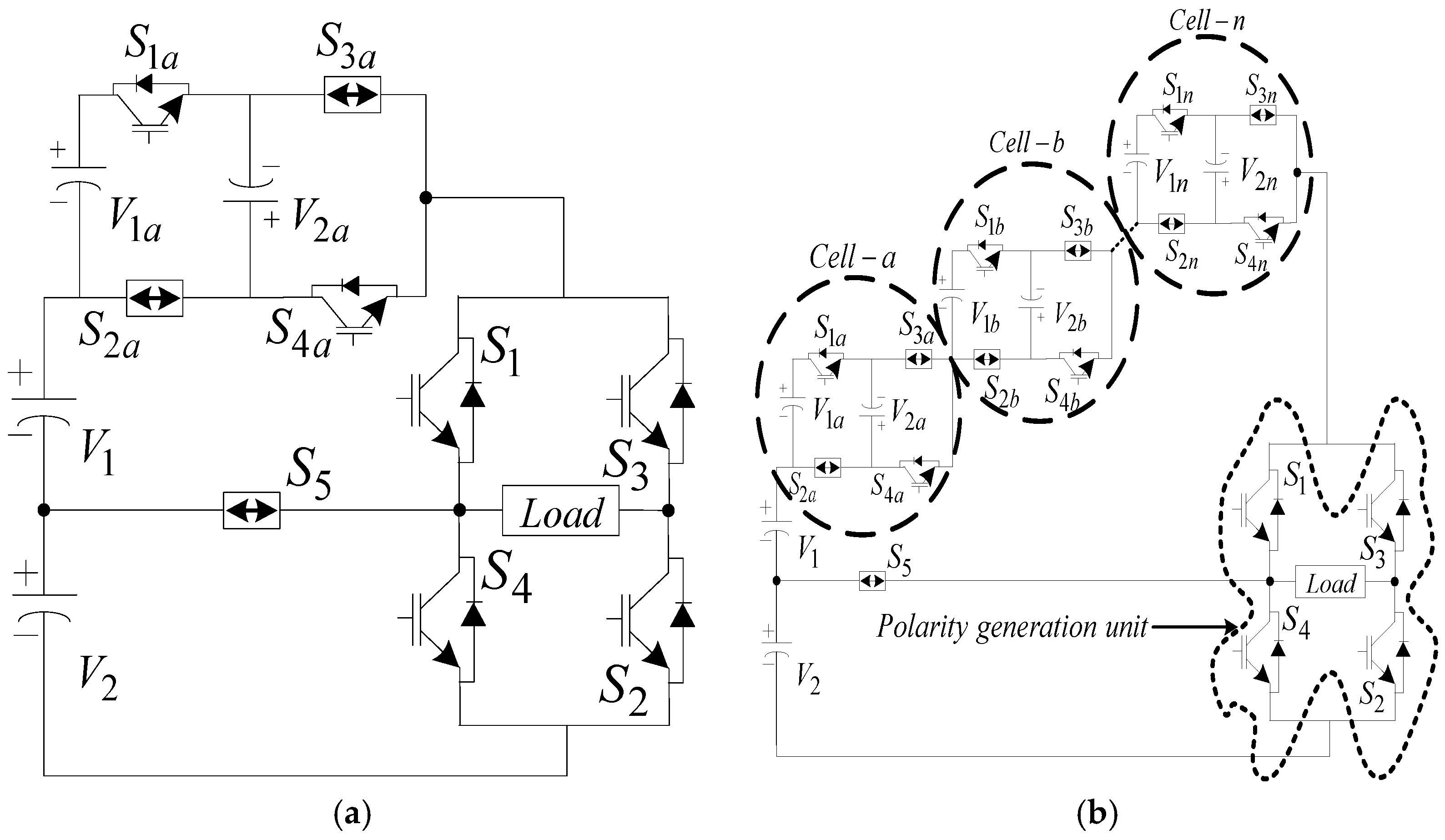
The proposed circuit−I is depicted in Figure 1a. First of all, the proposed topology consists of nine switches, generating nine level. The switches used are bi-directional and unidirectional. Bi-directional switches are employed for the flow of current in either direction. The unidirectional switches are S 1 , S 4 , S 5 , S 6 , S 7 ,   and   S whereas S 2 , S 3 , and S 9 are the bi-directional switches employed in the circuit. An H-bridge is employed for polarity generation, which contains four switches; in contrast, the rest of the circuit is used for level generation and contains five switches, as shown in Figure 1a. The MLI being symmetrical in nature, all the voltage magnitudes of the proposed MLI are the same. Therefore, a 9-level stepped output voltage can be generated only from one DC source. In Figure 1b, a generalized configuration of the proposed circuit is shown. It can be noticed that by adding only one bi-directional switch along with a capacitor, the attainment of the subsequent higher-voltage level is feasible. The minimum number of voltage levels achieved is nine when four capacitors of equal magnitudes and eight power switches are used. It can be noticed that by adding only one bi-directional switch along with a capacitor, the next higher-voltage level can be achieved. The minimum number of voltage levels achieved is nine when four capacitors of magnitude V 1 , V 2 , V 3 , V 4 = V dc and nine switches, S 1 , S 2 , S 3 , S 4 , S 5 , S 6 , S 7 , S 8 , S 9 , are used, where the switches S 5 , S 6 , S 7 , S 8 , S 9 are used to generate polarity, and the switches S 1 , S 2 , S 3 , S 4 are used to generate the voltage levels. Thus, the switches S 1 , S 2 , S 3 , S 4 , S 5 , S 6 , S 7 , S 8 , S 9 and the capacitors having magnitude V 1 , V 2 , V 3 , V 4 = V dc remain fixed throughout the overall topological structure. The only bi-directional switches and capacitors that are added to the existing circuit for generating the next higher-voltage level are S 1 , S 2 , S ( n 1 ) , S n and V 1 , V 2 , V n 1 , V n , respectively.
The addition of a bi-directional switch, S 1 and of a capacitor having voltage magnitude of V 1 generates nine voltage levels. Further, the addition of the switch S 2 with a capacitor next to the previous capacitor, having magnitude of V 2 , generates eleven levels. Moreover, a 13-level output voltage is generated by the further addition of the switch S 3 along with a capacitor having V 3 as the voltage magnitude. Thus, to generate the desired n-level output voltage, the switch S n is employed with a capacitor having V n as the voltage magnitude.

2.2. Circuit Operation of the Proposed Circuit-II

The proposed circuit−II contains nine switches, as shown in Figure 2a, of which six (S1, S2, S3, S4, S1a, S4a) are unidirectional, and three (S2a, S3a, S5) are bi-directional, with four capacitors (V1a, V2a, V1, V2). It consists of an H-bridge employing the switches S1, S2, S3, S4 that are generally used for polarity generation. As depicted in Figure 2b, cell-a, cell-b, etc., up to cell-n are enhanced as per the desired voltage levels to obtain the generalized configuration of circuit−II. There are two unidirectional and two bi-directional switches, along with two capacitors, in each cell unit, and these cells are cascaded to achieve higher levels, as depicted in Figure 2b. Thus, for generating the nth voltage level, a cascading of cells till the nth cell is required, which contains two bi-directional switches (S2n, S3n), two unidirectional switches (S1n, S4n), and two capacitors (V1n, V2n). Five switches (S1, S2, S3, S4, S5) and two capacitors (V1, V2) remain the same throughout the generalized proposed circuit−II.
Figure 3 shows the different types of arrangements for the bi-directional flow of current, depicted as (Figure 3a) Common Emitter IGBT, (Figure 3b) Diode Bridge with one Power Switch and (Figure 3c) Common Collector IGBT respectively. Considering the conduction loss point of view, the arrangements in Figure 3a,c seem to be better options than that in Figure 3b, as both of them contain only two diodes, whereas the configuration shown in Figure 3b has four diodes. When it comes to economic cost considerations, the arrangements in Figure 3a,c appear better than that in Figure 3b, as two driver circuits are needed to drive the bi-directional configuration shown in Figure 3c. Thus, taking the two parameters into account, the configuration depicted in Figure 3a, which ensures less conduction losses at an economical cost, is the better option and was chosen to be developed for the prototype model, employing one driver circuit with less conduction losses.
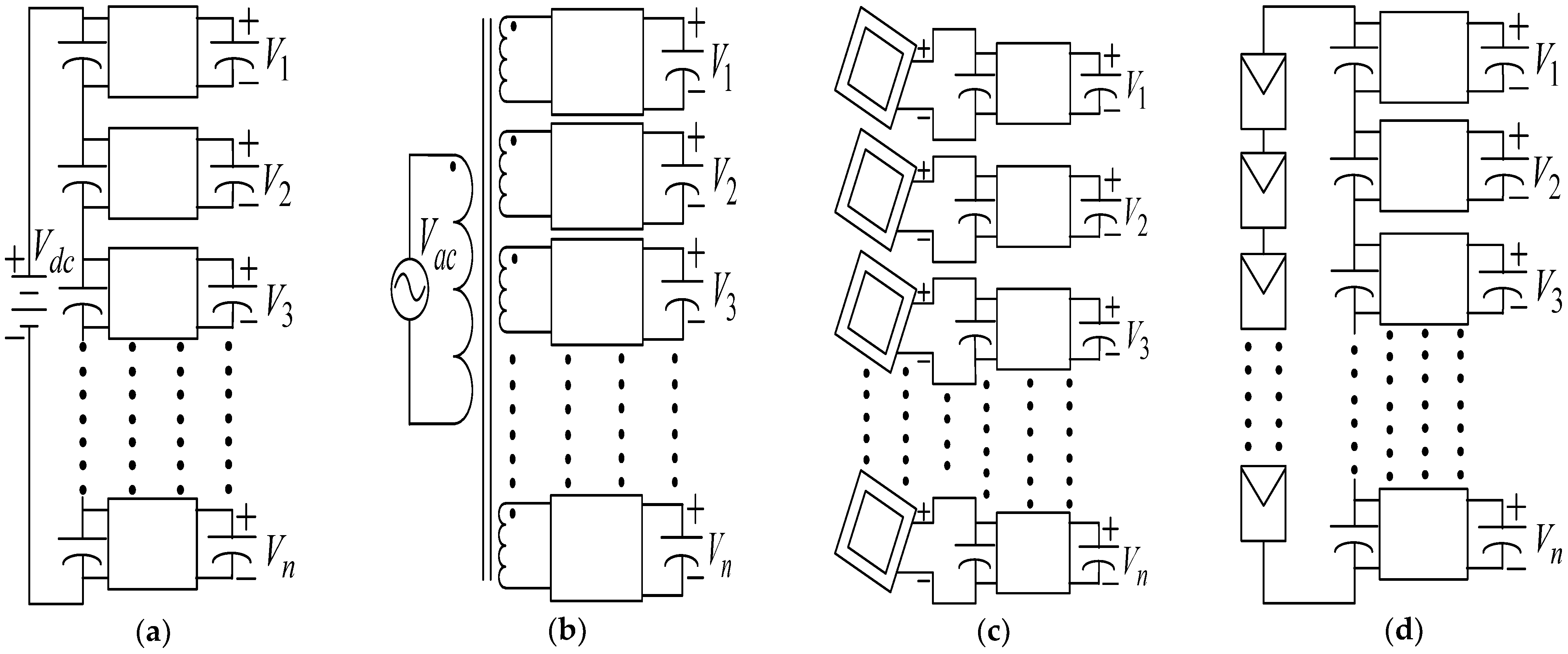
The various ways of providing a DC supply to capacitors are depicted in Figure 4a–c and 4d, respectively, where Vn is the nth voltage required to generate the nth output voltage levels.
There are four ways to provide DC voltages with the same magnitudes to capacitors, as follows:
  • One DC supply with DC/DC converters is employed for the required capacitors.
  • One AC supply is fed to the transformer primary side, with isolated multi-windings on the secondary side, then connected to a bridge rectifier, and fed to the required capacitors.
  • Every photovoltaic module is connected with DC/DC converters for the required capacitors.
  • Photovoltaic modules connected in series with DC/DC converters are employed for the required capacitors.

3. Modes of Operation

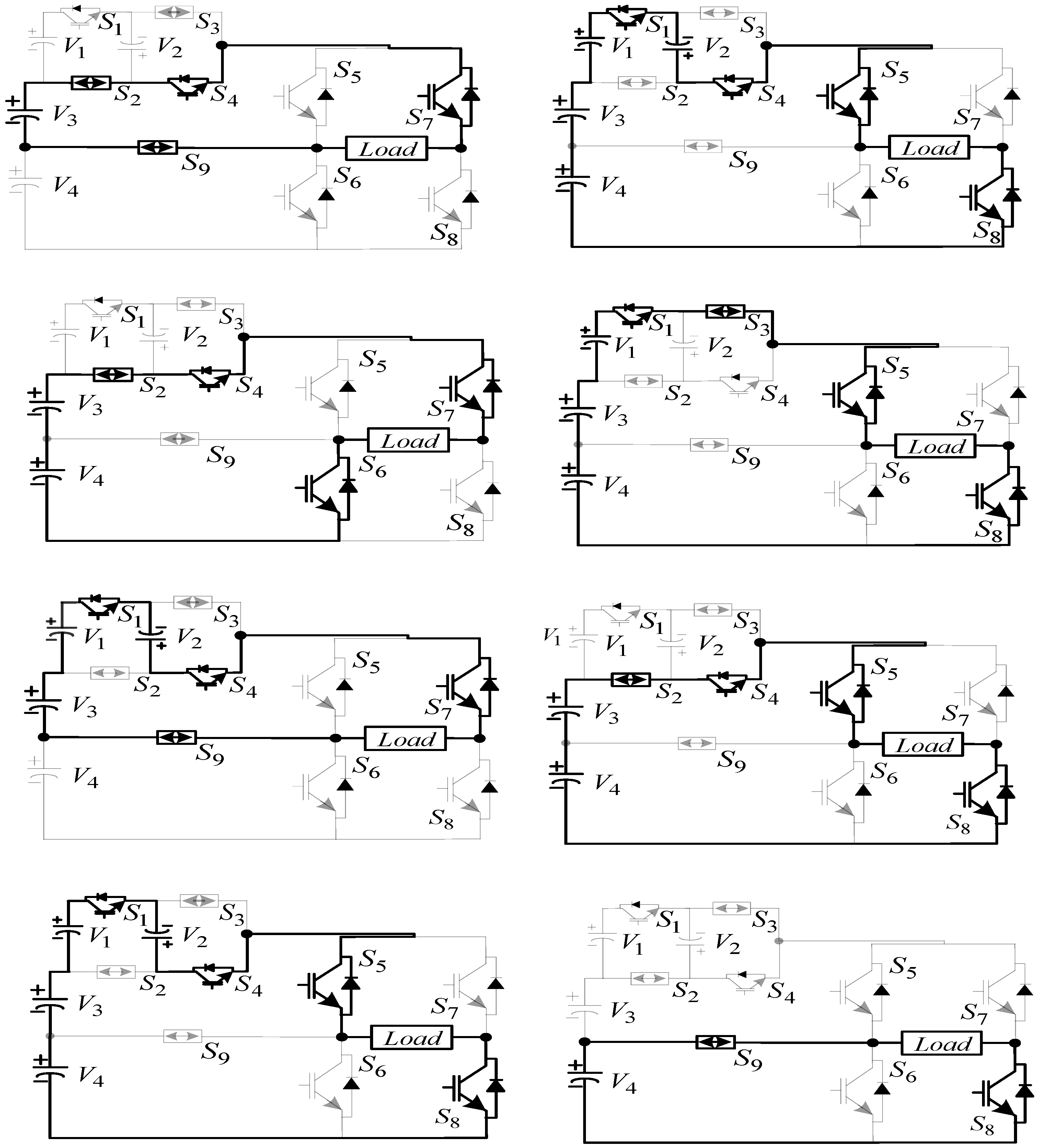
Various modes of operation in both the negative as well as the positive half cycle of the proposed 9-level circuit for circuit−I are depicted in Figure 5. It could be clearly noticed from the proposed topology depicted in Figure 1a and Figure 2a that the nomenclature of the components is only changed for the proposed inverter at the first stage, and therefore, the same components with different names (for circuit−I and circuit−II) generate different modes of voltage level.
The switching states of both the proposed circuit−I and circuit−II inverters are depicted in Table 1. One output voltage level is generated by each mode. For different modes of operation, the current paths were made thicker. Only four positive cycles, i.e., Mode-1, Mode-2, Mode-3, and Mode-4, generate +4Vdc, +3Vdc, +2Vdc, and +Vdc, respectively, whereas four negative cycles, i.e., Mode-6 (−Vdc), Mode-7 (−2Vdc), Mode-8 (−3Vdc), and Mode-9 (−4Vdc), produce four negative voltage output and are shown in Figure 5; the exception is Mode-5, with zero cycles.
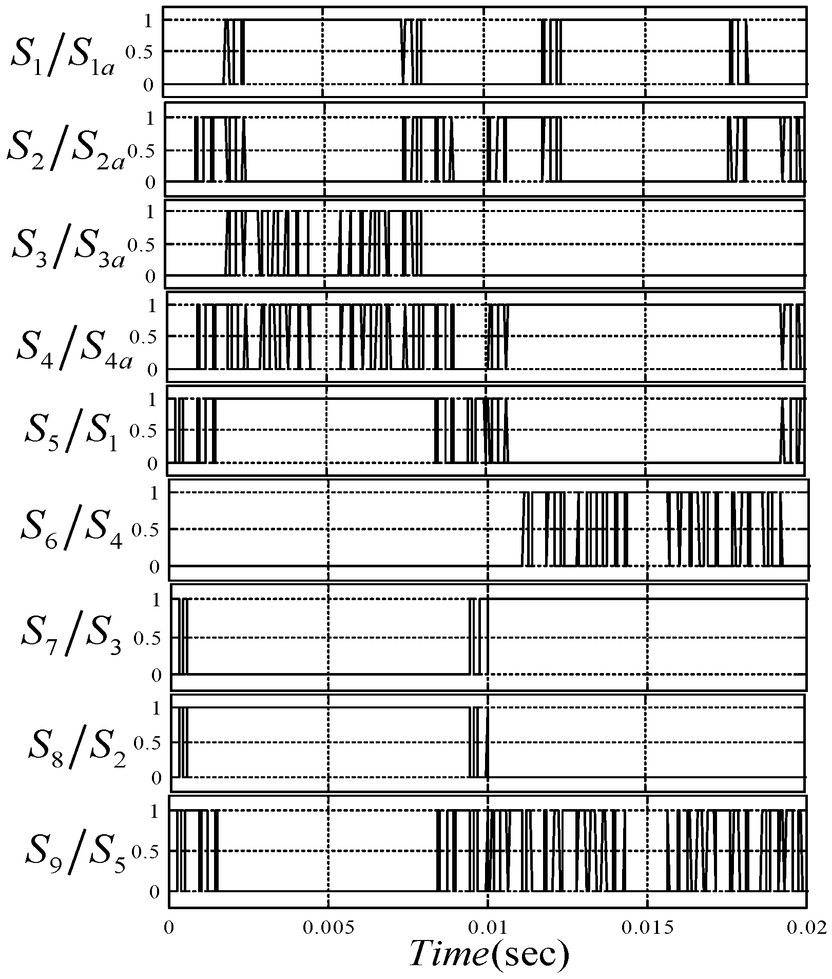
The pulse patterns generated using the dSPACE1103 controller by a carrier-based level-shifted PWM provided to the switches for the proposed 9-level MLI (for circuit−I and circuit−II) are depicted in Figure 6. This technique involves modulating the widths of the pulse signals based on a carrier wave and the desired output voltage levels, ensuring the efficient control of the semiconductor switches to attain the required voltage output.

4. Comparison with other MLI Topologies

In this section, several MLIs, including some recently proposed symmetric inverter topologies, are contrasted with the proposed topology. The generalized formulae for different topologies proposed in [24,25,26,27,28,29,30] are shown in Table 2 for various parameters such as total switches (M), gate driver circuits (N), capacitors/isolated DC sources (O), main diodes (P), unidirectional switches (Q), and bi-directional switches (R). In addition, parameters like the peak inverse voltage (PIV) across the power switch and the total standing voltage (TSV) of the inverter are included. The output voltage levels are denoted by NL.
The number of gate driver circuits required corresponds to the number of switches utilized, as each switch necessitates one driver circuit to generate a gate pulse. The main diodes are the ones associated with the switches. One anti-parallel diode is connected in the case of a unidirectional switches, whereas two or four diodes are associated with a bi-directional switch, as depicted in Figure 3.
Due to the aforesaid reasons, the configuration of the bi-directional switch proposed in Figure 3a was selected, and thus two diodes were considered for a bi-directional switch. The total component number was calculated based on the total number of switches, gate drivers, main diodes, and capacitors/DC used for the proposed inverter in this paper, as well as the configurations proposed [24,25,26,27,28,29,30].
All the aforementioned structures are shown in Figure 7. The MLI described in [24], requires two switches and a voltage source to achieve a level, which is then added in series to generate both positive and negative voltage levels with the use of an H-bridge. The configuration in [25] shows a single module with six switches and two DC sources that were used to generate the following voltage levels. In [26], a reduced-switch MLI with the optimal use of a DC link space is presented, where four switches and a DC source are required to produce the next level. As suggested in [27], two DC sources and four power semiconductor switches are combined to provide the subsequent voltage level. The MLIs proposed in [28,29,30] use several bi-directional switches, capacitors, and DC sources. In this paper, circuit−I generates the next voltage level through the addition of four switches with two DC sources. The proposed circuit−I and circuit−II generate higher-voltage levels using lesser power semiconductor switches in comparison with recent reduced-switch topologies [24,25,26,27,28,29,30].
The proposed topology (circuit−I and circuit−II) with a 9-level output, as detailed in Table 3, was thoroughly studied and compared with recently proposed topologies [24,25,26,27,28,29,30]. For the inverters proposed in [24,26], the required number of driving circuits and power switches was 16, 12, and 16, respectively, which was reduced to 9 switches (6 unidirectional and 3 bi-directional) in the proposed MLI topology. Comparing the proposed topology with the inverter introduced in [24,25,26,27], reductions in both power switches and driver circuits are observed. Due to the decrease in the number of power switches, the proposed topology is easier to construct, simpler to control, and more reliable.
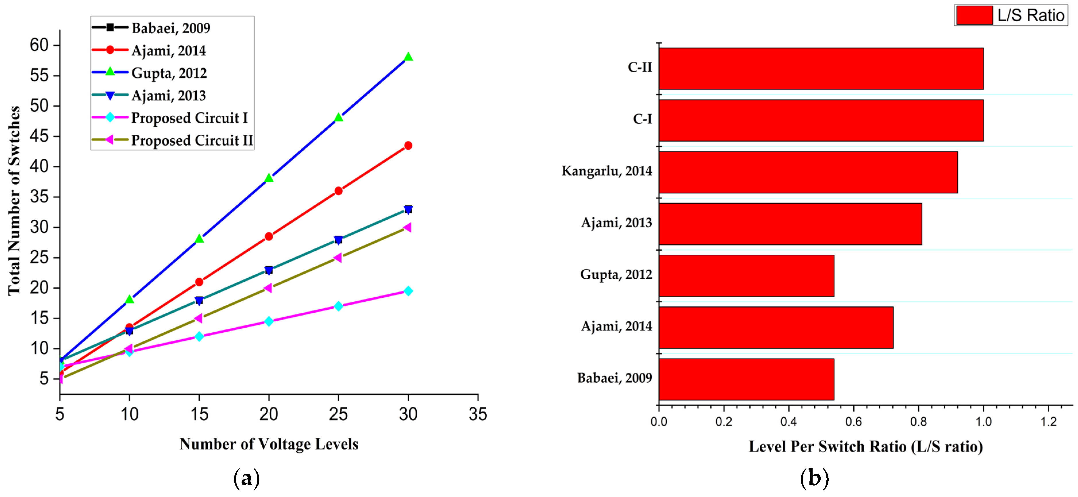
For all the considered parameters (M, N, O, P, Q, R), a graph was created comparing the topologies in [24,25,26,27,28,29,30] with the proposed topology, i.e., circuit−I and circuit−II, as depicted in Figure 8a. The graph evidently illustrates that the as the voltage levels increase, proposed topology requires fewer switches to achieve a voltage level, compared to the suggested MLIs in [24,25,26,27,28,29,30]. A new parameter known as the level-to-switch ratio (L/S ratio) was introduced to showcase the efficiency of the proposed MLI. The L/S ratio (phase voltage) denotes the required number of switches per output voltage level. The L/S ratio for a 13-level inverter is depicted in Figure 8b and was computed using Table 2. For an inverter, a higher L/S ratio is considered favorable, as higher levels of voltage can be achieved with the optimal number of or fewer switches. The magnitude of the L/S ratio for the proposed circuit−I (C-I) and circuit−II (C-II) are 1.18 and 1, respectively, and was much better than that of the inverters proposed in [24,25,26,27,28,29,30].
The TSV of the proposed MLI is relatively elevated, as illustrated in Table 3. However, the cost of the inverter is determined not solely by the TSV, but also by the PIV of each power switch. In spite of having a comparatively higher TSV, the inverter can be made economical by designing the inverter or selecting the components of the inverter in a hybrid model. The hybrid model of inverter implies that higher-rated power switches should be selected as the switches having a higher PIV, whereas lower-rated power switches should be selected as the switches having a lower PIV.
It should also be noted that only one PV source or one DC source is required for the suggested MLI topology. Considering the power switches, the proposed MLI requires only nine power switches (6 unidirectional and 3 bi-directional). Thus, a high TSV would not always have a negative impact on an inverter, especially when the MLI uses an H-bridge to generate polarity. These inverters, which create polarity via an H-bridge, have a positive impact on high-voltage applications. The proposed inverter is modular in structure and can also be cascaded in a modular fashion to achieve higher voltage, whereas inverters with self-polarity generation capability have a restricted application to a limited range of voltage levels or to higher voltages.

5. Simulation and Experimental Verification

A level-shifted SPWM was used to simulate the proposed topology (circuits I and II). The prototype model of the proposed MLI was developed in a laboratory utilizing a dSPACE-1103 controller. The prototype model utilizes the following components: a power switch (IGBT-CT60AM), gate driver circuits (TLP250), DSO-X 2024A, and an RL load, as shown in Figure 9.
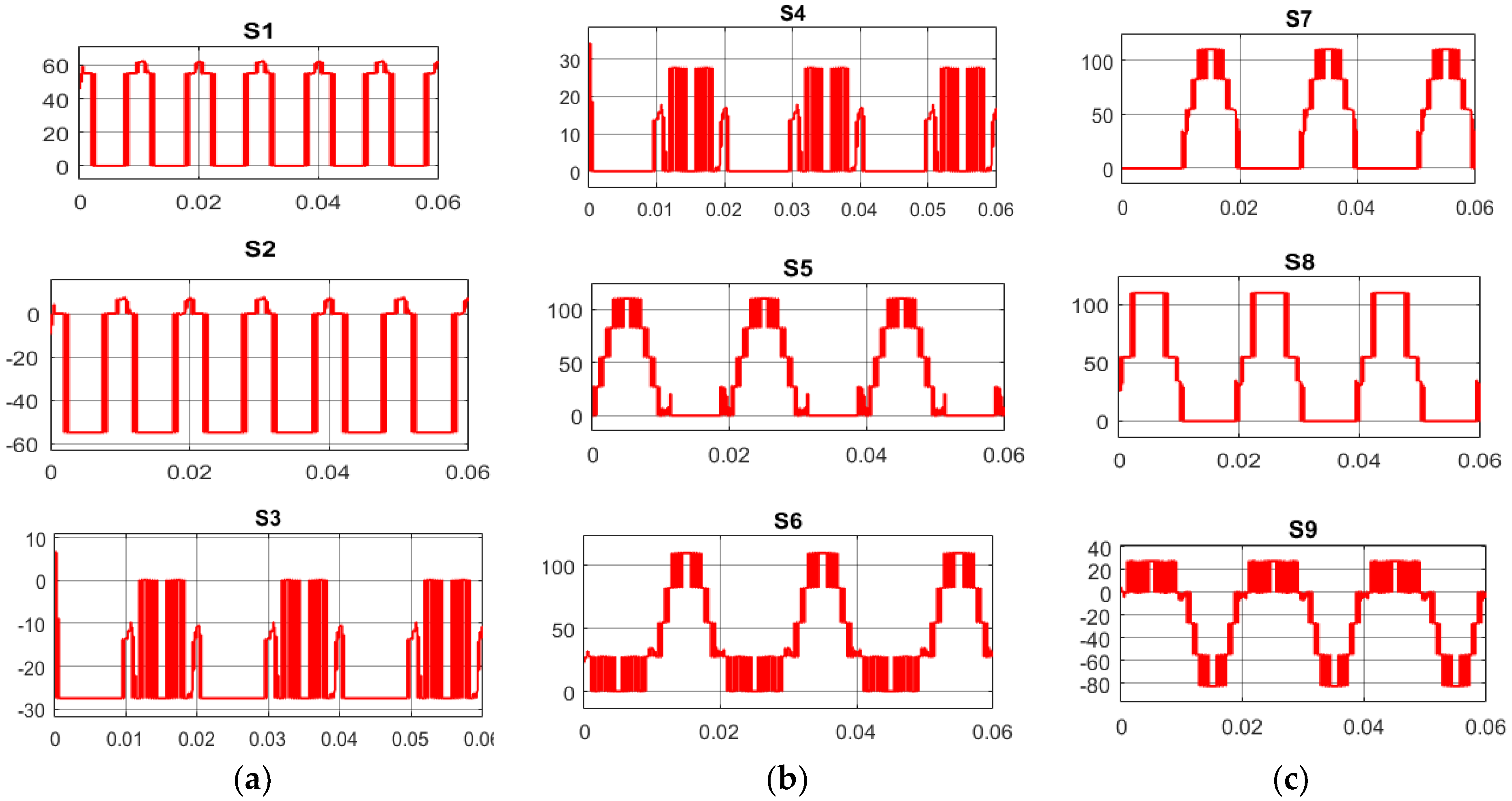
In MLIs, the term “blocking voltage” signifies the voltage threshold that every switching component, IGBTs or MOSFETs, must endure while in the inactive state. Surpassing the threshold can trigger the semiconductor breakdown, resulting in malfunction and potentially harming the entirety of the inverter system. Therefore, selecting switching devices with appropriate voltage ratings is crucial in multilevel inverter design to ensure reliability and safe operation. The blocking voltages across switches are depicted in Figure 10. The value of the blocking voltage across the switches S1, S2, and S3 are 60 V, 55 V, and 27.5 V, respectively, as shown in Figure 10a. Similarly, in Figure 10b, the blocking voltage of S4, S5, and S6 are depicted as 32 V, 110 V, and 110 V, respectively. As shown in Figure 10c, the values of the blocking voltage of S7, S8, and S9 are 110 V, 110 V, and −80 V, respectively.
The circuit parameters are included in Table 4 for both simulation and experimentation. For the basic 9-level inverter, taking into account parameters such the magnitude of all four capacitors with balanced voltages V1, V2, V3, V4 = 27.5 V, R = 200 Ω, and L = 150 mH at a fundamental frequency of 50 Hz, a prototype is shown. A switching frequency of 6 kHz resulted in an output voltage of 110 V and a load current of 0.71 A. A single DC source was used along with the DC/DC converter to provide equal values of DC magnitude, as shown in Figure 4a. The driver circuit utilized for each power switch is depicted in Figure 11, with the TLP250 serving as an opto-isolator.
All the simulated results for the 9-level inverter are presented in Figure 12 for the proposed circuit topology-I and circuit topology-II. The output voltage and output current of the proposed MLI were 110.3 V and 0.71 A, respectively, as depicted in Figure 12a. Figure 12b depicts the %THD of phase output voltage which was 13.52%.
Figure 13 depicts real-time switching pulses for the nine switches used in the proposed MLI, since the suggested configuration architecture was the same (circuit−I and circuit−II). The switching pulses of three switches, i.e., (S1, S2, S3); (S4, S5, S6); (S7, S8, S9), were grouped for 10 msec and are depicted in Figure 13a, Figure 13b, and Figure 13c, respectively. The switching pulse patterns of the switches present in circuit−II were similar to those in circuit−I, as shown in Figure 6.
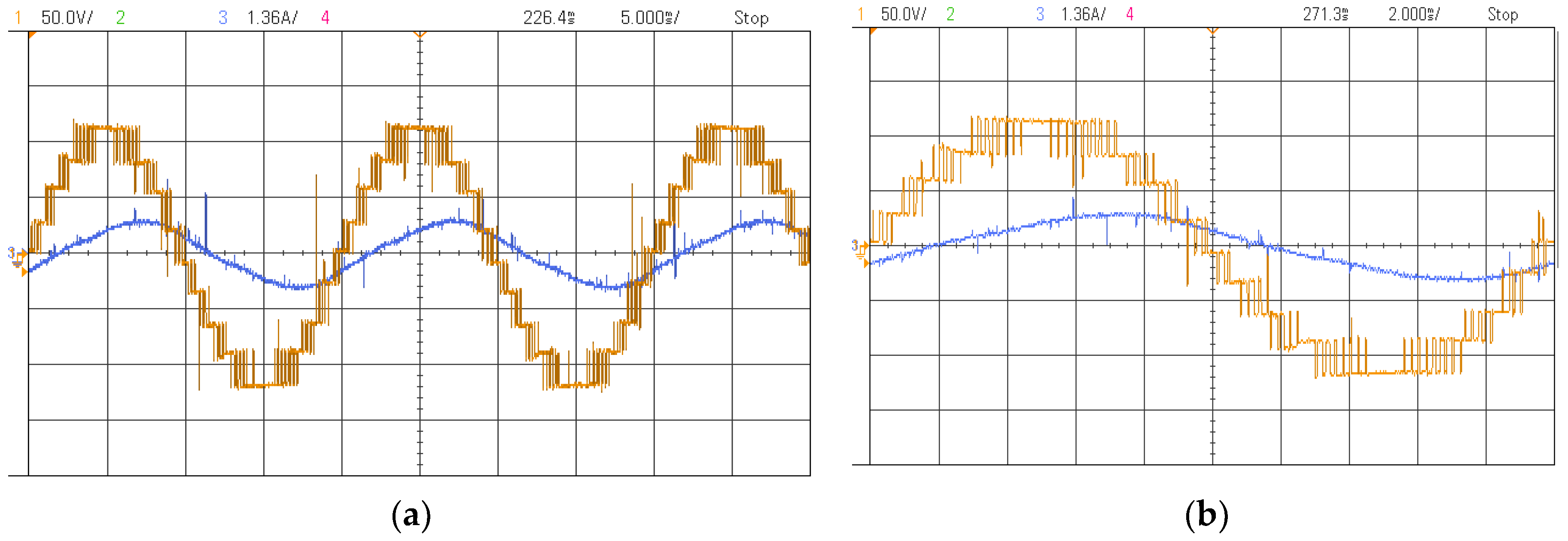
The experimental results for the 9-level have been shown in Figure 14, which validate the simulation results. Figure 14a depicts the experimental result for 2.5 cycles whereas Figure 14b depicts the for 1 complete cycle.
The experimentation and simulation are performed for 11-level output using the proposed circuit-I topology. As indicated in Table 4, for V1 = V2 = V3 = V4 = V5 = Vdc = 30 V with load values R = 200 Ω and L = 150 mH, the output voltage (peak) and output current are recorded as 145 V and 1.2 A respectively. The value of THD and the simulation output voltage are depicted in Figure 15a and corresponded to 145 V and 11.14%. For 13-level the simulation and the experimentation are performed using the proposed circuit-II topology. The simulation result for the output voltage and THD for 13-level of proposed circuit-II topology for V1 = V2 = V3 = V4 = V5 = V6 = Vdc = 21 V with load values R = 200 Ω and L = 100 mH have been shown in Figure 15b and corresponded to 125.7 V and 9.37% respectively.
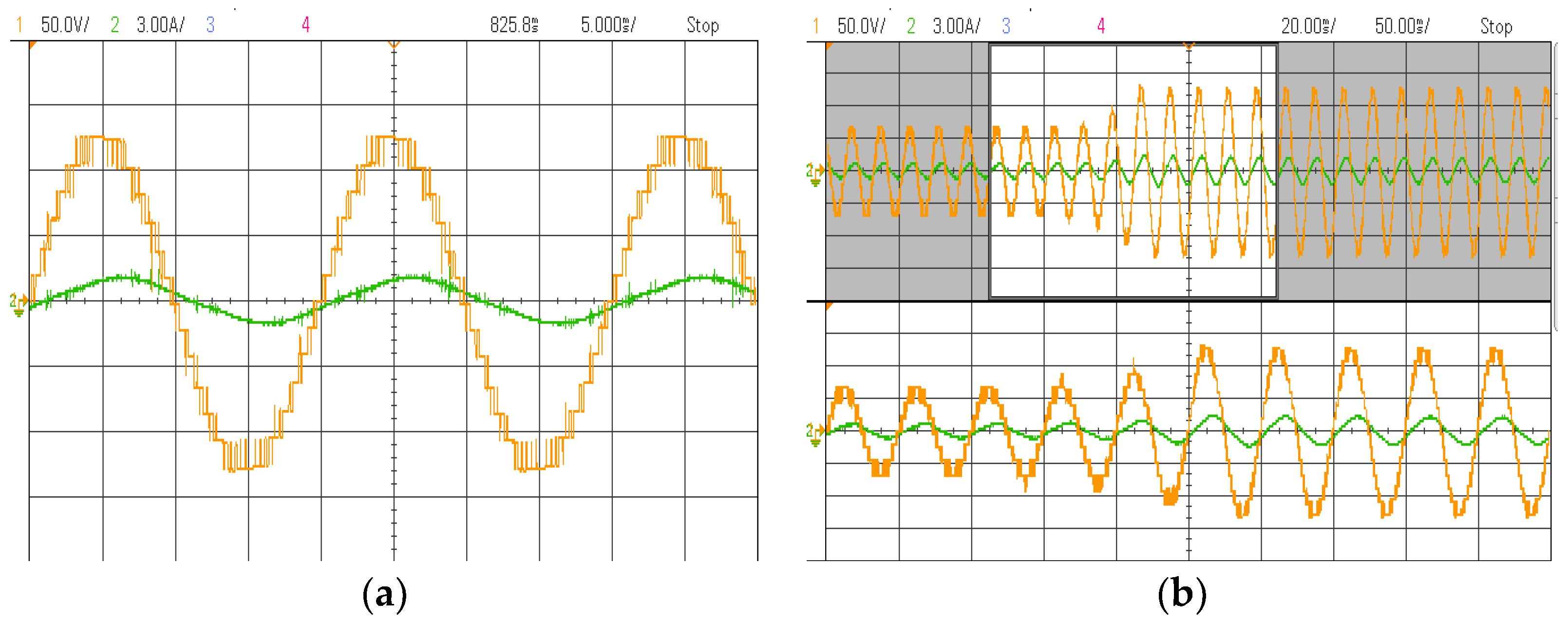
As mentioned earlier, experimentation and simulation are conducted for both an 11-level output and a 13-level output utilizing proposed circuit-I and proposed circuit-II topologies. The experimental results for the output voltage and load current for the 11-level topology and 13-level topology are depicted in Figure 16 and Figure 17, respectively. Figure 16a depicts the output voltage and load current for 11-level MLI for 2.5 cycles whereas Figure 16b depicts the output voltage and current for different modulation index. From the experimental results illustrated in Figure 16a, it is evident that the output voltage (peak) and load current (peak) for the 11-level setup are 145 V and 1.2 A, respectively, validating the simulation results.
Similarly, the experimental results for the 13-level configuration depicted in Figure 17a gives an output voltage (peak) and load current (peak) of 125.7 V and 1.2 A, respectively, further confirming the accuracy of the simulation results. Figure 17b depicts the output voltage and current for different modulation index for 13-level at different modulation index.

6. Conclusions

This work focused on a novel symmetrical MLI topology with fewer power semiconductor switches than those normally used. Both topologies, i.e., the proposed circuit−I and circuit−II were simulated in MATLAB/Simulink R2019b environment that used three bi-directional switches along with six unidirectional switches and four capacitors to generate a nine-level output. Both the proposed circuit topologies can be used in a generalized manner to generate an output of N levels. The DC supply can be fed to the capacitors in various ways, as explained in Section 2, whereas a single DC source is used along with a DC/DC converter to provide DC supply to the capacitors employed in this topology. Moreover, a single DC source can also be employed to obtain the same topology. The experimental outputs validated the simulation results of the 9-level suggested inverter. To generate nine-level voltage, the topology remained the same for both circuits. However, for output levels greater than nine, the two proposed topologies operate differently. The THD value obtained for the 9-level voltage was 13.52%. Further experimentation and simulation were performed for an 11-level output using the proposed circuit topology−I, yielding a THD value of 11.14%. Experimental and simulation analyses were also conducted for a 13-level output employing the proposed circuit topology−II, resulting in a THD value of 9.37%. Moreover, the comparisons (in the forms of charts as well as graphs) of the proposed inverter topologies with other recent MLI topologies as well as with classical topologies are presented. In the comparative study, it was evident that the proposed topology requires fewer components compared to the other cited topologies.

Author Contributions

Methodology, B.M.; Software, K.K.M.; Formal analysis, D.D. and M.M.; Investigation, P.D.; Resources, D.D., G.F. and V.V.; Data curation, M.M.; Writing—review & editing, B.C.; Supervision, B.M. All authors have read and agreed to the published version of the manuscript.

Funding

The authors acknowledge financial support for the dissemination of this work from the Special Account for Research of ASPETE through the funding program “Strengthening ASPETE’s research”.

Data Availability Statement

The data presented in this study are available in this article.

Conflicts of Interest

The authors declare no conflict of interest.

Correction Statement

This article has been republished with a minor correction to the Funding statement. This change does not affect the scientific content of the article.

References

  1. Jha, K.K.; Mahato, B.; Prakash, P.; Jana, K.C. Hardware Implementation of Single Phase Power Factor Correction System using Micro-controller. Int. J. Power Electron. Drive Syst. 2016, 7, 787–790. [Google Scholar]
  2. Rodriguez, J.; Franquelo, L.G.; Kouro, S.; Leon, J.I.; Portillo, R.C.; Prats, M.A.M.; Perez, M.A. Multilevel converters: An enabling technology for high-power applications. Proc. IEEE 2009, 97, 1786–1817. [Google Scholar] [CrossRef]
  3. Veenstra, M.; Rufer, A. Control of a hybrid asymmetric multilevel inverter for competitive medium-voltage industrial drives. IEEE Trans. Ind. Appl. 2005, 41, 655–664. [Google Scholar] [CrossRef]
  4. Franquelo, L.G.; Rodriguez, J.; Leon, J.I.; Kouro, S.; Portillo, R.; Prats, M.A. The age of multilevel converters arrives. IEEE Ind. Electron. Mag. 2008, 2, 28–39. [Google Scholar] [CrossRef]
  5. Mahato, B.; Mittal, S.; Nayak, P.K. Novel Topology of Multi-level Inverter for higher Voltage Steps. In Proceedings of the 2018 International Conference on Recent Trends in Electrical, Control and Communication (RTECC), Malaysia, 20–22 March 2018; pp. 158–163. [Google Scholar]
  6. Rodriguez, J.; Lai, J.S.; Peng, F.Z. Multilevel Inverters: A survey of topologies, controls, and applications. IEEE Trans. Ind. Electron. 2002, 49, 724–738. [Google Scholar] [CrossRef]
  7. Mahato, B.; Raushan, R.; Jana, K.C. Modulation and control of multilevel inverter for an open-end winding induction motor with constant voltage levels and harmonics. IET Power Electron. 2017, 10, 71–79. [Google Scholar] [CrossRef]
  8. Kouro, S.; Malinowski, M.; Gopakumar, K.; Pou, J.; Franquelo, L.G.; Wu, B.; Rodriguez, J.; Pérez, M.A.; Leon, J.I. Recent advances and industrial applications of multilevel converters. IEEE Trans. Ind. Electron. 2010, 57, 2553–2580. [Google Scholar] [CrossRef]
  9. Jana, K.C.; Jana, K.C.; Majumdar, S.; Pal, P.K.; Mahato, B. Performance Analysis of a Multimodule Staircase (MM-STC)-Type Multilevel Inverter with Reduced Component Count and Improved Efficiency. IEEE J. Emerg. Sel. Top. Power Electron. 2021, 10, 6619–6633. [Google Scholar]
  10. Lewicki, A.; Krzeminski, Z.; Abu-Rub, H. Space-vector pulsewidth modulation for three-level NPC converter with the neutral point voltage control. IEEE Trans. Ind. Electron. 2011, 58, 5076–5086. [Google Scholar] [CrossRef]
  11. Abu-Rub, H.; Malinowski, M.; Al-Haddad, K. Power Electronics for Renewable Energy Systems, Transportation and Industrial Applications; John Wiley & Sons: Hoboken, NJ, USA, 2014. [Google Scholar]
  12. Escalante, M.F.; Vannier, J.C.; Arzandé, A. Flying capacitor multilevel inverters and DTC motor drive applications. IEEE Trans. Ind. Electron. 2002, 49, 809–815. [Google Scholar] [CrossRef]
  13. Mahto, K.K.; Pal, P.K.; Das, P.; Mittal, S.; Mahato, B. A New Design of Multilevel Inverter Based on T-type Symmetrical and Asymmetrical DC Sources. Iran. J. Sci. Technol. Trans. Electr. Eng. 2022, 47, 639–657. [Google Scholar] [CrossRef]
  14. Nami, A.; Zare, F.; Ghosh, A.; Blaabjerg, F. A hybrid cascade converter topology with series-connected symmetrical and asymmetrical diode-clamped H-bridge cells. IEEE Trans. Power Electron. 2011, 26, 51–65. [Google Scholar] [CrossRef]
  15. Gupta, K.K.; Ranjan, A.; Bhatnagar, P.; Sahu, L.K.; Jain, S. Multilevel inverter topologies with reduced device count: A review. IEEE Trans. Power Electron. 2016, 31, 135–151. [Google Scholar] [CrossRef]
  16. Lezana, P.; Rodríguez, J.; Oyarzún, D.A. Cascaded multilevel inverter with regeneration capability and reduced number of switches. IEEE Trans. Ind. Electron. 2008, 55, 1059–1066. [Google Scholar] [CrossRef]
  17. Mahato, B.; Ranjan, M.; Pal, P.K.; Gupta, S.K.; Mahto, K.K. Design, development and verification of a new multilevel inverter for reduced power switches. Arch. Electr. Eng. 2022, 71, 1051–1063. [Google Scholar]
  18. Babaei, E.; Laali, S.; Bayat, Z. A single-phase cascaded multilevel inverter based on a new basic unit with reduced number of power switches. IEEE Trans. Ind. Electron. 2015, 62, 922–929. [Google Scholar] [CrossRef]
  19. Kangarlu, M.F.; Babaei, E. A generalized cascaded multilevel inverter using series connection of submultilevel inverters. IEEE Trans. Power Electron. 2013, 28, 625–636. [Google Scholar] [CrossRef]
  20. Dahidah, M.S.; Konstantinou, G.; Agelidis, V.G. A review of multilevel selective harmonic elimination PWM: Formulations, solving algorithms, implementation and applications. IEEE Trans. Power Electron. 2015, 30, 4091–4106. [Google Scholar] [CrossRef]
  21. Mahato, B.; Majumdar, S.; Jana, K.C. A new and generalized MLI with overall lesser power electronic devices. J. Circ. Syst. Comput. 2020, 29, 2050058. [Google Scholar] [CrossRef]
  22. Jana, K.C.; Biswas, S.K. Generalised switching scheme for a space vector pulse-width modulation-based N-level inverter with reduced switching frequency and harmonics. IET Power Electron. 2015, 8, 2377–2385. [Google Scholar]
  23. McGrath, B.P.; Holmes, D.G. Multicarrier PWM strategies for multilevel inverters. IEEE Trans. Ind. Electron. 2002, 49, 858–867. [Google Scholar] [CrossRef]
  24. Babaei, E.; Hosseini, S.H. New cascaded multilevel inverter topology with minimum number of switches. Energy Convers. Manag. 2009, 50, 2761–2767. [Google Scholar] [CrossRef]
  25. Ajami, A.; Oskuee, M.R.; Khosroshahi, M.T.; Mokhberdoran, A. Cascade-multi-cell multilevel converter with reduced number of switches. IET Power Electron. 2014, 7, 2914–2924. [Google Scholar] [CrossRef]
  26. Gupta, K.K.; Jain, S. Topology for multilevel inverters to attain maximum number of levels from given DC sources. IET Power Electron. 2012, 5, 435–446. [Google Scholar] [CrossRef]
  27. Ajami, A.; Oskuee, M.R.J.; Mokhberdoran, A.; Van den Bossche, A. Developed cascaded multilevel inverter topology to minimise the number of circuit devices and voltage stresses of switches. IET Power Electron. 2013, 7, 459–466. [Google Scholar] [CrossRef]
  28. Gautam, S.P.; Kumar, L.; Gupta, S. Hybrid topology of symmetrical multilevel inverter using less number of devices. IET Power Electron. 2015, 8, 2125–2135. [Google Scholar] [CrossRef]
  29. Kangarlu, M.F.; Babaei, E. Cross-switched multilevel inverter: An innovative topology. IET Power Electron. 2014, 6, 642–651. [Google Scholar] [CrossRef]
  30. Alishah, R.S.; Nazarpour, D.; Hosseini, S.H.; Sabahi, M. Reduction of Power Electronic Elements in Multilevel Converters Using a New Cascade Structure. IEEE Trans. Ind. Electron. 2014, 62, 256–269. [Google Scholar] [CrossRef]
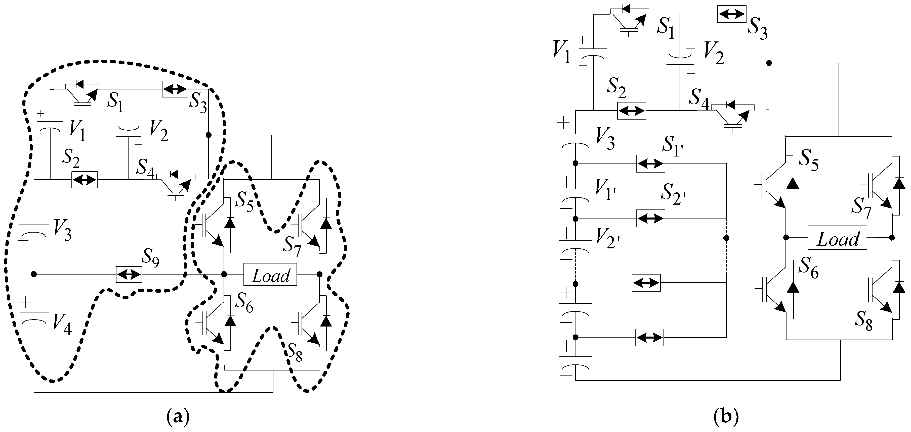
Figure 1. Proposed topology: (a) proposed circuit−I topology; (b) generalized proposed circuit−I topology.
Electronics 13 01975 g001
Figure 2. Proposed topology: (a) proposed circuit−II topology; (b) generalized proposed circuit−II topology.
Electronics 13 01975 g002
Figure 3. Different types of configurations of bi-directional switches (a) Common Emitter; IGBT (b) Diode Bridge with one Power Switch (c) Common Collector IGBT.
Electronics 13 01975 g003
Figure 4. Different ways to generate DC voltages for the capacitors.
Electronics 13 01975 g004
Figure 5. Operating modes for the fundamental structural topology (circuit−I or circuit−II).
Electronics 13 01975 g005
Figure 6. Generated pulse pattern for the proposed inverter (circuit−I and circuit−II) for 9-level output voltage.
Electronics 13 01975 g006
Figure 7. Circuits of the compared topologies proposed in (a) [24]; (b) [25]; (c) [26]; (d) [27]; (e) [28]; (f) [29]; (g) [30].
Electronics 13 01975 g007
Figure 8. Comparison of the proposed topology with existing topologies in terms of (a) total number of switches required for different voltage level; (b) level-per-switch ratio [24,25,26,27,29].
Electronics 13 01975 g008
Figure 9. Experimental set-up in the laboratory for the proposed MLI.
Electronics 13 01975 g009
Figure 10. Blocking voltages across the switches: (a) S1, S2, and S3; (b) S4, S5, and S6; (c) S7, S8, and S9.
Electronics 13 01975 g010
Figure 11. Gate driver circuit for a power switch.
Electronics 13 01975 g011
Figure 12. Simulation results for the 9-level inverter: (a) output voltage and current; (b) %THD of output phase voltage.
Electronics 13 01975 g012aElectronics 13 01975 g012b
Figure 13. Switching pulses fed to the power switches of the proposed circuit−I topology: (a) S1, S2 and S3; (b) S3, S4, and S5; (c) S6, S7, and S8.
Electronics 13 01975 g013
Figure 14. Load voltage and current for the 9-level inverter: (a) 2.5 cycles; (b) 1 cycle.
Electronics 13 01975 g014
Figure 15. Total harmonic distortion of the output voltage of the proposed inverters: (a) 11−level inverter; (b) 13−level inverter.
Electronics 13 01975 g015
Figure 16. Load voltage and current for the 11-level inverter; (a) 2.5 cycles; (b) different modulation indices.
Electronics 13 01975 g016
Figure 17. Load voltage and current for the 13-level inverter: (a) 2.5 cycles; (b) different modulation indices.
Electronics 13 01975 g017
Table 1. Switching states of the proposed 9-level inverter.
ModesSwitching States
1 = ON; 0 = OFF
Circuit−I
Voltages
Circuit−II
Voltages
Stepped Output Voltage
Generation
Circuit−I S 1 S 2 S 3 S 4 S 5 S 6 S 7 S 8 S 9 V 1 = V 2 = V d c
V 3 = V 4 = V d c
V 1 a = V 2 a = V d c
V 1 = V 2 = V d c
Circuit−II S 1 a S 2 a S 3 a S 4 a S 1 S 4 S 3 S 2 S 5
Mode-1100110010 V 1 + V 2 + V 3 + V 4 V 1 a + V 2 a + V 1 + V 2 + 4 V d c
Mode-2101010010 V 1 + V 3 + V 4 V 1 a + V 1 + V 2 + 3 V d c
Mode-3010110010 V 3 + V 4 V 1 + V 2 + 2 V d c
Mode-4000000011 V 4 V 2 + V d c
Mode-5000010100------ + 0 V d c
000001010------ + 0 V d c
Mode-6010100101 V 3 V 1 V d c
Mode-7010101100 V 3 + V 4 V 1 + V 2 2 V d c
Mode-8100100101 V 1 + V 2 + V 3 V 1 a + V 2 a + V 1 3 V d c
Mode-9100101100 V 1 + V 2 + V 3 + V 4 V 1 a + V 2 a + V 1 + V 2 4 V d c
Table 2. Comparison chart of the generalized formulations.
MLI Compared with the Proposed TopologyTotal Switches
(M)
Gate Driver Circuit (N)Capacitors/Isolated DC Sources (O)Main Diodes
(P)
Switches
Unidirectional
Switches (Q)
Bi-Directional
Switches (R)
[24] 2 ( N L 1 ) 2 ( N L 1 ) ( N L 1 ) 2 2 ( N L 1 ) 2 ( N L 1 ) ---
[25] 3 ( N L 1 ) 2 3 ( N L 1 ) 2 ( N L 1 ) 2 3 ( N L 1 ) 2 3 ( N L 1 ) 2 ---
[26] 2 ( N L 1 ) 2 ( N L 1 ) ( N L 1 ) 2 2 ( N L 1 ) 2 ( N L 1 ) ---
[27] ( N L + 3 ) ( N L + 3 ) ( N L 1 ) 2 ( N L + 3 ) ( N L + 3 ) ---
[28] 7 ( N L 1 ) / 8 7 ( N L 1 ) / 8 ( N L 1 ) 2 ( N L 1 ) 8 ( N L 1 ) 8 3 ( N L 1 ) 4
[29] N L + 1 N L + 1 ( N L 1 ) 2 N L + 1 N L + 1 ---
[30] ( N L + 5 ) / 2 ( N L + 5 ) / 2 ( N L 1 ) 2 44 ( N L 3 ) / 2
Proposed Circuit−I Topology ( N L + 9 ) 2 ( N L + 9 ) 2 ( N L 1 ) 2 ( N L + 3 ) 6 ( N L 3 ) 2
Proposed Circuit−II Topology N L N L ( N L 1 ) 2 3 ( N L 1 ) 2 ( N L + 3 ) 2 ( N L 3 ) 2
Table 3. Comparison of the proposed inverter with recent topologies.
Cited PapersVoltage Levels
N L
Total Switches
(M)
Capacitors/Isolated DC Sources
(O)
PIV
(Peak Inverse Voltage)
TSV
(Total Standing Voltage)
[24]91644 Vdc24 Vdc
[25]9124Vdc12 Vdc
[26]91643 Vdc24 Vdc
[27]9124Vdc12 Vdc
[28]9742 Vdc13 Vdc
[29]91044 Vdc16 Vdc
[30]9743 Vdc20 Vdc
Circuit−I and Circuit−II Topology9944 Vdc24 Vdc
Table 4. Circuit parameters in the simulation and experimental tests and outputs at different levels.
ParametersName and Value or Type
Switching parameters IGBTCT-60AM-18F: 900 V, 60 A
Von, IGBT = 1.3 V, Von, Dio = 1.5 V, RDio = 0.01Ω, RIGBT = 0.11Ω, β = 3
Types of switching devices and their controlling elementsDiode
driver
Controller, switching frequency
MUR1560G: 600 V, 15 A
TLP250: 10–35, ±1.5 A
DS1103, 6 kHz
Common parameters of simulation and
experimental tests
9-level inverter (same for circuit−I topology and circuit−II topologies)
(V1 = V2 = V3 = V4 = Vdc = 27.5 V)
R = 200 Ω, L = 150 mH, Vpk = 110.3 V, Ipk = 0.71 A.
11-level inverter, (Circuit−I Topology)
(V1 = V2 = V3 = V4 = V5 = Vdc = 30 V)
R = 200 Ω, L = 100 mH, Vpk = 145 V, Ipk = 1.2 A.
13-level inverter, (circuit−II topology)
(V1 = V2 = V3 = V4 = V5 = V6 = Vdc = 21 V)
R = 200 Ω, L = 100 mH, Vpk = 125.7 V, Ipk = 1.2 A.
Disclaimer/Publisher’s Note: The statements, opinions and data contained in all publications are solely those of the individual author(s) and contributor(s) and not of MDPI and/or the editor(s). MDPI and/or the editor(s) disclaim responsibility for any injury to people or property resulting from any ideas, methods, instructions or products referred to in the content.